EP0945783A2 - Dispositif de registres de longueur variable - Google Patents
Dispositif de registres de longueur variable Download PDFInfo
- Publication number
- EP0945783A2 EP0945783A2 EP99105020A EP99105020A EP0945783A2 EP 0945783 A2 EP0945783 A2 EP 0945783A2 EP 99105020 A EP99105020 A EP 99105020A EP 99105020 A EP99105020 A EP 99105020A EP 0945783 A2 EP0945783 A2 EP 0945783A2
- Authority
- EP
- European Patent Office
- Prior art keywords
- variable length
- bits
- registers
- length register
- register
- Prior art date
- Legal status (The legal status is an assumption and is not a legal conclusion. Google has not performed a legal analysis and makes no representation as to the accuracy of the status listed.)
- Withdrawn
Links
Images


Classifications
-
- G—PHYSICS
- G06—COMPUTING OR CALCULATING; COUNTING
- G06F—ELECTRIC DIGITAL DATA PROCESSING
- G06F9/00—Arrangements for program control, e.g. control units
- G06F9/06—Arrangements for program control, e.g. control units using stored programs, i.e. using an internal store of processing equipment to receive or retain programs
- G06F9/30—Arrangements for executing machine instructions, e.g. instruction decode
- G06F9/30003—Arrangements for executing specific machine instructions
- G06F9/30007—Arrangements for executing specific machine instructions to perform operations on data operands
- G06F9/30032—Movement instructions, e.g. MOVE, SHIFT, ROTATE, SHUFFLE
-
- G—PHYSICS
- G06—COMPUTING OR CALCULATING; COUNTING
- G06F—ELECTRIC DIGITAL DATA PROCESSING
- G06F9/00—Arrangements for program control, e.g. control units
- G06F9/06—Arrangements for program control, e.g. control units using stored programs, i.e. using an internal store of processing equipment to receive or retain programs
- G06F9/30—Arrangements for executing machine instructions, e.g. instruction decode
- G06F9/30003—Arrangements for executing specific machine instructions
- G06F9/30007—Arrangements for executing specific machine instructions to perform operations on data operands
- G06F9/3001—Arithmetic instructions
- G06F9/30014—Arithmetic instructions with variable precision
-
- G—PHYSICS
- G06—COMPUTING OR CALCULATING; COUNTING
- G06F—ELECTRIC DIGITAL DATA PROCESSING
- G06F9/00—Arrangements for program control, e.g. control units
- G06F9/06—Arrangements for program control, e.g. control units using stored programs, i.e. using an internal store of processing equipment to receive or retain programs
- G06F9/30—Arrangements for executing machine instructions, e.g. instruction decode
- G06F9/30098—Register arrangements
- G06F9/30105—Register structure
- G06F9/30112—Register structure comprising data of variable length
Definitions
- the invention relates to a register device used in a computer as a temporary memory device, and especially to a variable length register device, a register length and the number of the registers of which are variable.
- variable length register device is composed of the first selector, which selects lower n bits of the first register of N bits (N>n) and outputs them, the second selector, which selects upper N-n bits of the first register of N bits (N>n) and output them, and an operational circuit, which is supplied with the outputs of the first and second selectors and outputs data of N bits by carrying out an operation of logical OR.
- This variable length register device is used in case that a memory can be effectively utilized by changing a bank address of the memory by a software.
- variable length register device disclosed in Japanese patent Kokai 4-76748, since an used area in the register cannot be dermined in accordance with the length of the data, the use thereof is restricted to assignment of the bank address of the memory and does not attain to a general register.
- the determination of the register length and the number of the registers have important meanings in the design of the processor architecture. If insufficiency in the registers occurs at the time of a process of a application, the throughput deteriorates. If redundant registers are provided, the cost of the processor increases. In case of application that data of 32 bits is necessary sometimes, but only lower 16 or 8 bits are necessary for the process many times, the number of utilized bits is far smaller than that of the necessary registers, and there arise lots of futility.
- variable length register device which can be utilized not only for assigning addresses in memory but also as a general register.
- an variable length register comprises:
- Fig.1 is a block diagram for showing a variable length register device according to a preferred embodiment of the invention.
- variable length register device 1 a variable length resister 2, 4-1 selectors 3 and an arithmetic logical unit (an ALU, hereinafter) 4 and a 4-1 selector 5 are successively connected in this order to form a loop, and an instruction memory 6, an instruction decoder 7 and a sequencer 8 are successively connected in this order to form another loop.
- a part of an output of the ALU 4 is supplied to the sequencer 8, and an instruction decoded by the instruction decoder 7 is supplied to the variable length resister 2, the 4-1 selectors 3, the ALU 4 and the 4-1 selector 5.
- the variable length resister device is connected with an external circuit via an external interface 10 and a control bus 11.
- An instruction to gain access to the variable length register 2 is outputted from the instruction memory 6, and inputted to the instruction decoder 7 to be decoded.
- a control signal for specifying the variable length register 2 and assigning an used area therein is generated in the instruction decoder 7, transmitted to the variable length decoder 2, the 4-1 selectors 3, the ALU 4 and the 4-1 selector 5, and inputted to the sequencer 8.
- Data in the variable length resister 2 is read on the 4-1 selectors 3 and the used areas therein are coordinated in accordance the instruction supplied from the instruction decoder 7. Then, the data are inputted to the ALU 4 and operated therein. The operated data is read on the 4-1 selector 5 and the used areas therein are coordinated. The data in the 4-1 selector 5 is again written into the variable length register 2. At this time, various flags are transmitted to the sequencer 8, and following instructions are executed.
- FIG.2 shows an example of assignment of the used areas.
- a register with a length of 32 bits is assigned as variable length registers of 8/16/24/32 bits. In this case, it is sometimes necessary that every 8 bits is provided with a read/write enable terminal in accordance with the structure of a hardware of the register.
- the used area having the name of B0 covers 8 bits corresponding to the 0th to 7th bit
- the same having the name of B1 covers 8 bits corresponding to the 8th to 15th bit
- the same having the name of B2 covers 8 bits corresponding to the 16th to the 23rd bit
- the same having the name of B3 covers 8 bits corresponding to the 24th to 31st bit.
- the used area having the name of H0 covers 16 bits corresponding to the 0th to the 15th bit
- the same having the name of H1 covers 16 bits corresponding to the 16th to the 31st bit.
- the used area having the name of Q0 covers 24 bits corresponding to the 0th to the 23rd bit.
- the used areas having the name of W0 covers 32 bits corresponding to the 0th to the 31st bit.
- the name of the used area is expressed by a binary code of 3 bits.
- the assignment of the used area in the variable length register 2 is specified in the instruction to gain access to the variable length register 2, and, in such a case, the name of the used area (the binary code, in case of a machine word) should be combined with a operand.
- a discriminator for specifying a variable length register 2 to be used in the several ones is combined with the discriminator for assigning the used area.
- a method for assigning the used area in the variable length register 2, the number of the variable length resisters and the use of the fixed length register jointly with the variable register are suitably selected in consideration of a target of application.
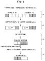
- FIG.3 shows the operation of the variable length register device 1 concretely.
- Step S1 the data in the n th B3 area of the variable length register 2 of the source A and the data in the m th H0 area in the variable length register 2 of the source B are respectively read on the 4-1 selectors 3 (Step S1), and the used areas are coordinated. Since the source A assigns the B3 area (8 bits corresponding to the 24th to the 31st bit), the data stored therein is closely shifted to the B0 area (8 bits corresponding to the 0th to the 7th bit) and "0" is stored in the unused area (24 bits corresponding to the 8th to the 31st bit), before the data is inputted to the ALU 4.
- Step S2 since the source B assigns the H0 area (16 bits corresponding to the 0th to the 15th bit), the data stored therein is not shifted to the right, but "0" is stored in the unused area (16 bits corresponding to the 16th to the 31st bit) (Step S2).
- the data, the used areas of which have been coordinated, are inputted to the ALU 4 and arithmetically added together, and various flags generated as the result of the operation are transmitted to the sequencer 8.
- a carry occurs at the position of the 16th bit (Step 3).
- the arithmetically added data is read on the 4-1 selector 5, and the used area is coordinated. That is to say, since the destination register assigns the H1 area (16 bits corresponding to the 16th to the 31st bit), the data is shifted to the H1 area (16 bits corresponding to the 16th to the 31st bit) from the H0 area (16 bits corresponding to the 0th to the 15th bit). Finally, the data, the used area of which has been coordinated, is stored in the destination register. It is enough to renew the data stored in the H1 area (Step 4).
- variable length register device 1 having a structure mentioned in the above, the numbers of the registers in the variable length register 2 can be optimized, even in case that the process becomes redundant by adopting the fixed length registers in some characteristic of application.
- the data when the four data, in each of which only lower 8 bits are truly necessary, are read, the data must be read four times in case that the fixed length registers of 32 bits are used, and shift/mask is necessary in accordance with the structure of a hardware.
- the four data, each being composed of 8 bits are previously stored in the variable length register of 32 bits, read can be completed at a time, so that the times of accesses can be reduced and the throughput can be improved.
- variable length register can be exhibited in case that an external memory is jointly used.
- the data can be transmitted to the internal register via a 32 bit bus and the four data, each being composed of 8 bits, stored in the 32 bit external memory are read, it is necessary to adopt a method that four data, each being composed of 8 bits, are respectively stored in that lower 8 nits of four words in the 32 bit external memory, and these data are taken into the lower 8 bits of four words of the 32 bit fixed length registers through accesses of four times; or another method that the four data, each being composed of 8 bits, are stored in one word of the 32 bit external memory, and the data are taken into one word of the 32 bit fixed length register at a time and read four times, where sift, mask and etc. are necessary in accordance with a structure of a hardware.
- the four data are stored into one word of the 32 bit external memory, and the data are taken into the 32 bit variable length register at a time, so that excessive operations can be reduced and the throughput can be improved.
- variable length register device since the length of the register and the number of the registers are variable, consumed electrical power can be reduced.
- the length of the register and the number of the registers are variable, plural information can be stored in a single register, the times of accesses can be reduced, and, as the result, the throughput is improved and consumed electrical power is cut down.
Landscapes
- Engineering & Computer Science (AREA)
- Software Systems (AREA)
- Theoretical Computer Science (AREA)
- Physics & Mathematics (AREA)
- General Physics & Mathematics (AREA)
- General Engineering & Computer Science (AREA)
- Computational Mathematics (AREA)
- Mathematical Analysis (AREA)
- Mathematical Optimization (AREA)
- Pure & Applied Mathematics (AREA)
- Executing Machine-Instructions (AREA)
- Memory System (AREA)
Applications Claiming Priority (2)
| Application Number | Priority Date | Filing Date | Title |
|---|---|---|---|
| JP10073939A JPH11272546A (ja) | 1998-03-23 | 1998-03-23 | 可変長レジスタ装置 |
| JP7393998 | 1998-03-23 |
Publications (2)
| Publication Number | Publication Date |
|---|---|
| EP0945783A2 true EP0945783A2 (fr) | 1999-09-29 |
| EP0945783A3 EP0945783A3 (fr) | 2001-09-26 |
Family
ID=13532597
Family Applications (1)
| Application Number | Title | Priority Date | Filing Date |
|---|---|---|---|
| EP99105020A Withdrawn EP0945783A3 (fr) | 1998-03-23 | 1999-03-19 | Dispositif de registres de longueur variable |
Country Status (3)
| Country | Link |
|---|---|
| EP (1) | EP0945783A3 (fr) |
| JP (1) | JPH11272546A (fr) |
| CA (1) | CA2266259A1 (fr) |
Cited By (12)
| Publication number | Priority date | Publication date | Assignee | Title |
|---|---|---|---|---|
| WO2002029553A1 (fr) * | 2000-10-04 | 2002-04-11 | Arm Limited | Traitement à instruction unique données multiples |
| WO2002017072A3 (fr) * | 2000-08-23 | 2002-10-17 | Chipwrights Design Inc | Appareil et procede d'utilisation de pointeurs a etiquette destines a des operations d'extraction, d'insertion et de formatage |
| US6732253B1 (en) | 2000-11-13 | 2004-05-04 | Chipwrights Design, Inc. | Loop handling for single instruction multiple datapath processor architectures |
| GB2406418A (en) * | 2003-09-26 | 2005-03-30 | Samsung Electronics Co Ltd | A memory with data buffers in which the buffer width is varied based upon redundant fields in the address supplied to the memory |
| US6931518B1 (en) | 2000-11-28 | 2005-08-16 | Chipwrights Design, Inc. | Branching around conditional processing if states of all single instruction multiple datapaths are disabled and the computer program is non-deterministic |
| EP1825383A4 (fr) * | 2004-11-17 | 2009-12-23 | Sandbridge Technologies Inc | Fichier de donnees stockant des types de donnees multiples avec un acces aux donnees controle |
| WO2012069798A1 (fr) * | 2010-11-23 | 2012-05-31 | Arm Limited | Appareil de traitement de données ayant une instruction de manipulation de champ binaire et procédé |
| US9069938B2 (en) | 2006-11-03 | 2015-06-30 | Bluerisc, Inc. | Securing microprocessors against information leakage and physical tampering |
| US9235393B2 (en) | 2002-07-09 | 2016-01-12 | Iii Holdings 2, Llc | Statically speculative compilation and execution |
| US9569186B2 (en) | 2003-10-29 | 2017-02-14 | Iii Holdings 2, Llc | Energy-focused re-compilation of executables and hardware mechanisms based on compiler-architecture interaction and compiler-inserted control |
| US9697000B2 (en) | 2004-02-04 | 2017-07-04 | Iii Holdings 2, Llc | Energy-focused compiler-assisted branch prediction |
| US20220164190A1 (en) * | 2020-05-27 | 2022-05-26 | Blaize, Inc. | Method of optimizing scalar register allocation and a system thereof |
Families Citing this family (4)
| Publication number | Priority date | Publication date | Assignee | Title |
|---|---|---|---|---|
| JP3560596B2 (ja) | 2002-08-22 | 2004-09-02 | 沖電気工業株式会社 | 演算装置及びデータの読出方法 |
| US7996671B2 (en) | 2003-11-17 | 2011-08-09 | Bluerisc Inc. | Security of program executables and microprocessors based on compiler-architecture interaction |
| JP5003070B2 (ja) * | 2006-09-09 | 2012-08-15 | ヤマハ株式会社 | デジタル信号処理装置 |
| JP5375114B2 (ja) * | 2009-01-16 | 2013-12-25 | 富士通株式会社 | プロセッサ |
Family Cites Families (2)
| Publication number | Priority date | Publication date | Assignee | Title |
|---|---|---|---|---|
| US5590352A (en) * | 1994-04-26 | 1996-12-31 | Advanced Micro Devices, Inc. | Dependency checking and forwarding of variable width operands |
| US6175892B1 (en) * | 1998-06-19 | 2001-01-16 | Hitachi America. Ltd. | Registers and methods for accessing registers for use in a single instruction multiple data system |
-
1998
- 1998-03-23 JP JP10073939A patent/JPH11272546A/ja active Pending
-
1999
- 1999-03-19 EP EP99105020A patent/EP0945783A3/fr not_active Withdrawn
- 1999-03-22 CA CA 2266259 patent/CA2266259A1/fr not_active Abandoned
Cited By (26)
| Publication number | Priority date | Publication date | Assignee | Title |
|---|---|---|---|---|
| US6678806B1 (en) | 2000-08-23 | 2004-01-13 | Chipwrights Design, Inc. | Apparatus and method for using tagged pointers for extract, insert and format operations |
| WO2002017072A3 (fr) * | 2000-08-23 | 2002-10-17 | Chipwrights Design Inc | Appareil et procede d'utilisation de pointeurs a etiquette destines a des operations d'extraction, d'insertion et de formatage |
| WO2002029553A1 (fr) * | 2000-10-04 | 2002-04-11 | Arm Limited | Traitement à instruction unique données multiples |
| US6999985B2 (en) | 2000-10-04 | 2006-02-14 | Arm Limited | Single instruction multiple data processing |
| RU2279706C2 (ru) * | 2000-10-04 | 2006-07-10 | Арм Лимитед | Обработка с использованием одного потока команд и множества потоков данных |
| US6732253B1 (en) | 2000-11-13 | 2004-05-04 | Chipwrights Design, Inc. | Loop handling for single instruction multiple datapath processor architectures |
| US6931518B1 (en) | 2000-11-28 | 2005-08-16 | Chipwrights Design, Inc. | Branching around conditional processing if states of all single instruction multiple datapaths are disabled and the computer program is non-deterministic |
| US10101978B2 (en) | 2002-07-09 | 2018-10-16 | Iii Holdings 2, Llc | Statically speculative compilation and execution |
| US9235393B2 (en) | 2002-07-09 | 2016-01-12 | Iii Holdings 2, Llc | Statically speculative compilation and execution |
| GB2406418A (en) * | 2003-09-26 | 2005-03-30 | Samsung Electronics Co Ltd | A memory with data buffers in which the buffer width is varied based upon redundant fields in the address supplied to the memory |
| GB2406418B (en) * | 2003-09-26 | 2005-12-21 | Samsung Electronics Co Ltd | Circuits and methods for providing variable data I/O width for semiconductor memory devices |
| US10248395B2 (en) | 2003-10-29 | 2019-04-02 | Iii Holdings 2, Llc | Energy-focused re-compilation of executables and hardware mechanisms based on compiler-architecture interaction and compiler-inserted control |
| US9569186B2 (en) | 2003-10-29 | 2017-02-14 | Iii Holdings 2, Llc | Energy-focused re-compilation of executables and hardware mechanisms based on compiler-architecture interaction and compiler-inserted control |
| US9697000B2 (en) | 2004-02-04 | 2017-07-04 | Iii Holdings 2, Llc | Energy-focused compiler-assisted branch prediction |
| US10268480B2 (en) | 2004-02-04 | 2019-04-23 | Iii Holdings 2, Llc | Energy-focused compiler-assisted branch prediction |
| KR101371931B1 (ko) * | 2004-11-17 | 2014-03-10 | 퀄컴 인코포레이티드 | 제어된 데이터 액세스를 이용하여 다중 데이터 타입을 저장하는 데이터 파일 |
| EP1825383A4 (fr) * | 2004-11-17 | 2009-12-23 | Sandbridge Technologies Inc | Fichier de donnees stockant des types de donnees multiples avec un acces aux donnees controle |
| US9069938B2 (en) | 2006-11-03 | 2015-06-30 | Bluerisc, Inc. | Securing microprocessors against information leakage and physical tampering |
| US9940445B2 (en) | 2006-11-03 | 2018-04-10 | Bluerisc, Inc. | Securing microprocessors against information leakage and physical tampering |
| US10430565B2 (en) | 2006-11-03 | 2019-10-01 | Bluerisc, Inc. | Securing microprocessors against information leakage and physical tampering |
| US11163857B2 (en) | 2006-11-03 | 2021-11-02 | Bluerisc, Inc. | Securing microprocessors against information leakage and physical tampering |
| US9619225B2 (en) | 2010-11-23 | 2017-04-11 | Arm Limited | Apparatus and method including an instruction for performing a logical operation on a repeating data value generated based on data size and control parameter portions specified by the instruction |
| US9207937B2 (en) | 2010-11-23 | 2015-12-08 | Arm Limited | Apparatus and method for processing a bitfield manipulation instruction having a control value indicating insertion or extraction form |
| WO2012069798A1 (fr) * | 2010-11-23 | 2012-05-31 | Arm Limited | Appareil de traitement de données ayant une instruction de manipulation de champ binaire et procédé |
| US10521232B2 (en) | 2010-11-23 | 2019-12-31 | Arm Limited | Data processing apparatus and method for processing a SIMD instruction specifying a control value having a first portion identifying a selected data size and a second portion identifying at least one control parameter having a number of bits that varies in dependence on a number of bits comprised by the first portion |
| US20220164190A1 (en) * | 2020-05-27 | 2022-05-26 | Blaize, Inc. | Method of optimizing scalar register allocation and a system thereof |
Also Published As
| Publication number | Publication date |
|---|---|
| CA2266259A1 (fr) | 1999-09-23 |
| JPH11272546A (ja) | 1999-10-08 |
| EP0945783A3 (fr) | 2001-09-26 |
Similar Documents
| Publication | Publication Date | Title |
|---|---|---|
| EP0945783A2 (fr) | Dispositif de registres de longueur variable | |
| US6205534B1 (en) | Apparatus and method for processing data with a plurality of flag groups | |
| US5893143A (en) | Parallel processing unit with cache memories storing NO-OP mask bits for instructions | |
| US7363466B2 (en) | Microcomputer | |
| US6408377B2 (en) | Dynamic allocation of resources in multiple microprocessor pipelines | |
| US20010008563A1 (en) | Parallel processor and image processing apparatus | |
| KR100465388B1 (ko) | Risc 구조의 8비트 마이크로 제어기 | |
| US5577256A (en) | Data driven type information processor including a combined program memory and memory for queuing operand data | |
| US6378050B1 (en) | Information processing apparatus and storage medium | |
| US6578139B1 (en) | Processor architecture scheme which uses virtual address registers to implement different addressing modes and method therefor | |
| US5440714A (en) | Method and system configuration for simplifying the decoding system for access to an register file with overlapping windows | |
| EP0636986A2 (fr) | Décodeur d'adresse à petite échelle de circuit et à possibilité d'extension de zone d'adresse | |
| US5740458A (en) | Protocol processor intended for the execution of a collection of instructions in a reduced number of operations | |
| US7047396B1 (en) | Fixed length memory to memory arithmetic and architecture for a communications embedded processor system | |
| JP2551167B2 (ja) | マイクロコンピュータ | |
| JPH09231071A (ja) | コンピュータ装置 | |
| EP0383342A2 (fr) | Microprocesseur | |
| US6779098B2 (en) | Data processing device capable of reading and writing of double precision data in one cycle | |
| US20040024992A1 (en) | Decoding method for a multi-length-mode instruction set | |
| US6081869A (en) | Bit-field peripheral | |
| US6772271B2 (en) | Reduction of bank switching instructions in main memory of data processing apparatus having main memory and plural memory | |
| US7370179B2 (en) | Microprocessor | |
| US20040162965A1 (en) | Information processing unit | |
| US6000026A (en) | Multiple processor apparatus having a protocol processor intended for the execution of a collection of instructions in a reduced number of operations | |
| EP0328422A2 (fr) | Système micro-ordinateur |
Legal Events
| Date | Code | Title | Description |
|---|---|---|---|
| PUAI | Public reference made under article 153(3) epc to a published international application that has entered the european phase |
Free format text: ORIGINAL CODE: 0009012 |
|
| AK | Designated contracting states |
Kind code of ref document: A2 Designated state(s): AT BE CH CY DE DK ES FI FR GB GR IE IT LI LU MC NL PT SE Kind code of ref document: A2 Designated state(s): DE FR GB |
|
| AX | Request for extension of the european patent |
Free format text: AL;LT;LV;MK;RO;SI |
|
| PUAL | Search report despatched |
Free format text: ORIGINAL CODE: 0009013 |
|
| AK | Designated contracting states |
Kind code of ref document: A3 Designated state(s): AT BE CH CY DE DK ES FI FR GB GR IE IT LI LU MC NL PT SE |
|
| AX | Request for extension of the european patent |
Free format text: AL;LT;LV;MK;RO;SI |
|
| 17P | Request for examination filed |
Effective date: 20010814 |
|
| AKX | Designation fees paid |
Free format text: DE FR GB |
|
| STAA | Information on the status of an ep patent application or granted ep patent |
Free format text: STATUS: THE APPLICATION HAS BEEN WITHDRAWN |
|
| 18W | Application withdrawn |
Withdrawal date: 20020823 |