EP0945938A2 - Elektrisches Pumpen von mit seltenen Erden dotiertem Silizium für optische Emission - Google Patents
Elektrisches Pumpen von mit seltenen Erden dotiertem Silizium für optische Emission Download PDFInfo
- Publication number
- EP0945938A2 EP0945938A2 EP99301326A EP99301326A EP0945938A2 EP 0945938 A2 EP0945938 A2 EP 0945938A2 EP 99301326 A EP99301326 A EP 99301326A EP 99301326 A EP99301326 A EP 99301326A EP 0945938 A2 EP0945938 A2 EP 0945938A2
- Authority
- EP
- European Patent Office
- Prior art keywords
- rare
- earth element
- region
- type region
- junction
- Prior art date
- Legal status (The legal status is an assumption and is not a legal conclusion. Google has not performed a legal analysis and makes no representation as to the accuracy of the status listed.)
- Granted
Links
- 229910052710 silicon Inorganic materials 0.000 title claims description 11
- 239000010703 silicon Substances 0.000 title claims description 11
- 230000003287 optical effect Effects 0.000 title description 5
- 238000005086 pumping Methods 0.000 title 1
- 229910052761 rare earth metal Inorganic materials 0.000 claims abstract description 29
- 239000004065 semiconductor Substances 0.000 claims abstract description 16
- 239000002800 charge carrier Substances 0.000 claims abstract description 12
- 229910052691 Erbium Inorganic materials 0.000 claims description 6
- UYAHIZSMUZPPFV-UHFFFAOYSA-N erbium Chemical compound [Er] UYAHIZSMUZPPFV-UHFFFAOYSA-N 0.000 claims description 6
- 238000000034 method Methods 0.000 claims description 5
- 229910052779 Neodymium Inorganic materials 0.000 claims description 3
- 238000010894 electron beam technology Methods 0.000 claims description 3
- QEFYFXOXNSNQGX-UHFFFAOYSA-N neodymium atom Chemical compound [Nd] QEFYFXOXNSNQGX-UHFFFAOYSA-N 0.000 claims description 3
- 229910052777 Praseodymium Inorganic materials 0.000 claims 2
- PUDIUYLPXJFUGB-UHFFFAOYSA-N praseodymium atom Chemical compound [Pr] PUDIUYLPXJFUGB-UHFFFAOYSA-N 0.000 claims 2
- 230000004913 activation Effects 0.000 claims 1
- 238000004519 manufacturing process Methods 0.000 abstract 1
- XUIMIQQOPSSXEZ-UHFFFAOYSA-N Silicon Chemical compound [Si] XUIMIQQOPSSXEZ-UHFFFAOYSA-N 0.000 description 9
- 239000002019 doping agent Substances 0.000 description 5
- 239000000758 substrate Substances 0.000 description 5
- 238000010586 diagram Methods 0.000 description 4
- 230000004048 modification Effects 0.000 description 4
- 238000012986 modification Methods 0.000 description 4
- 150000002910 rare earth metals Chemical class 0.000 description 4
- 239000004020 conductor Substances 0.000 description 3
- 230000005693 optoelectronics Effects 0.000 description 3
- 230000006798 recombination Effects 0.000 description 3
- 238000005215 recombination Methods 0.000 description 3
- VYPSYNLAJGMNEJ-UHFFFAOYSA-N Silicium dioxide Chemical compound O=[Si]=O VYPSYNLAJGMNEJ-UHFFFAOYSA-N 0.000 description 2
- 229910052782 aluminium Inorganic materials 0.000 description 2
- 229910052785 arsenic Inorganic materials 0.000 description 2
- 239000000969 carrier Substances 0.000 description 2
- 238000005401 electroluminescence Methods 0.000 description 2
- 229910052733 gallium Inorganic materials 0.000 description 2
- 229910052738 indium Inorganic materials 0.000 description 2
- 238000002347 injection Methods 0.000 description 2
- 239000007924 injection Substances 0.000 description 2
- 238000000752 ionisation method Methods 0.000 description 2
- 239000000463 material Substances 0.000 description 2
- 230000007246 mechanism Effects 0.000 description 2
- 230000000737 periodic effect Effects 0.000 description 2
- PFNQVRZLDWYSCW-UHFFFAOYSA-N (fluoren-9-ylideneamino) n-naphthalen-1-ylcarbamate Chemical compound C12=CC=CC=C2C2=CC=CC=C2C1=NOC(=O)NC1=CC=CC2=CC=CC=C12 PFNQVRZLDWYSCW-UHFFFAOYSA-N 0.000 description 1
- JBRZTFJDHDCESZ-UHFFFAOYSA-N AsGa Chemical compound [As]#[Ga] JBRZTFJDHDCESZ-UHFFFAOYSA-N 0.000 description 1
- GYHNNYVSQQEPJS-UHFFFAOYSA-N Gallium Chemical compound [Ga] GYHNNYVSQQEPJS-UHFFFAOYSA-N 0.000 description 1
- 229910001218 Gallium arsenide Inorganic materials 0.000 description 1
- 229910000577 Silicon-germanium Inorganic materials 0.000 description 1
- BGZYUAAGFXBZMA-UHFFFAOYSA-N [Pr].[Er] Chemical compound [Pr].[Er] BGZYUAAGFXBZMA-UHFFFAOYSA-N 0.000 description 1
- LEVVHYCKPQWKOP-UHFFFAOYSA-N [Si].[Ge] Chemical compound [Si].[Ge] LEVVHYCKPQWKOP-UHFFFAOYSA-N 0.000 description 1
- 238000010521 absorption reaction Methods 0.000 description 1
- 229910045601 alloy Inorganic materials 0.000 description 1
- 239000000956 alloy Substances 0.000 description 1
- XAGFODPZIPBFFR-UHFFFAOYSA-N aluminium Chemical compound [Al] XAGFODPZIPBFFR-UHFFFAOYSA-N 0.000 description 1
- 229910052787 antimony Inorganic materials 0.000 description 1
- RQNWIZPPADIBDY-UHFFFAOYSA-N arsenic atom Chemical compound [As] RQNWIZPPADIBDY-UHFFFAOYSA-N 0.000 description 1
- 230000002860 competitive effect Effects 0.000 description 1
- 150000001875 compounds Chemical class 0.000 description 1
- 229910003460 diamond Inorganic materials 0.000 description 1
- 239000010432 diamond Substances 0.000 description 1
- 230000005684 electric field Effects 0.000 description 1
- 239000000835 fiber Substances 0.000 description 1
- 229910052732 germanium Inorganic materials 0.000 description 1
- GNPVGFCGXDBREM-UHFFFAOYSA-N germanium atom Chemical compound [Ge] GNPVGFCGXDBREM-UHFFFAOYSA-N 0.000 description 1
- BHEPBYXIRTUNPN-UHFFFAOYSA-N hydridophosphorus(.) (triplet) Chemical compound [PH] BHEPBYXIRTUNPN-UHFFFAOYSA-N 0.000 description 1
- APFVFJFRJDLVQX-UHFFFAOYSA-N indium atom Chemical compound [In] APFVFJFRJDLVQX-UHFFFAOYSA-N 0.000 description 1
- 230000003993 interaction Effects 0.000 description 1
- 238000005468 ion implantation Methods 0.000 description 1
- 230000001404 mediated effect Effects 0.000 description 1
- 238000004377 microelectronic Methods 0.000 description 1
- 229910052698 phosphorus Inorganic materials 0.000 description 1
- HBMJWWWQQXIZIP-UHFFFAOYSA-N silicon carbide Chemical compound [Si+]#[C-] HBMJWWWQQXIZIP-UHFFFAOYSA-N 0.000 description 1
- 229910010271 silicon carbide Inorganic materials 0.000 description 1
- 239000000377 silicon dioxide Substances 0.000 description 1
- 239000000243 solution Substances 0.000 description 1
- 230000000638 stimulation Effects 0.000 description 1
- 230000007704 transition Effects 0.000 description 1
Images

Classifications
-
- H—ELECTRICITY
- H10—SEMICONDUCTOR DEVICES; ELECTRIC SOLID-STATE DEVICES NOT OTHERWISE PROVIDED FOR
- H10H—INORGANIC LIGHT-EMITTING SEMICONDUCTOR DEVICES HAVING POTENTIAL BARRIERS
- H10H20/00—Individual inorganic light-emitting semiconductor devices having potential barriers, e.g. light-emitting diodes [LED]
- H10H20/80—Constructional details
- H10H20/81—Bodies
- H10H20/822—Materials of the light-emitting regions
- H10H20/826—Materials of the light-emitting regions comprising only Group IV materials
- H10H20/8262—Materials of the light-emitting regions comprising only Group IV materials characterised by the dopants
-
- H—ELECTRICITY
- H10—SEMICONDUCTOR DEVICES; ELECTRIC SOLID-STATE DEVICES NOT OTHERWISE PROVIDED FOR
- H10H—INORGANIC LIGHT-EMITTING SEMICONDUCTOR DEVICES HAVING POTENTIAL BARRIERS
- H10H20/00—Individual inorganic light-emitting semiconductor devices having potential barriers, e.g. light-emitting diodes [LED]
- H10H20/80—Constructional details
- H10H20/81—Bodies
- H10H20/813—Bodies having a plurality of light-emitting regions, e.g. multi-junction LEDs or light-emitting devices having photoluminescent regions within the bodies
-
- H—ELECTRICITY
- H01—ELECTRIC ELEMENTS
- H01S—DEVICES USING THE PROCESS OF LIGHT AMPLIFICATION BY STIMULATED EMISSION OF RADIATION [LASER] TO AMPLIFY OR GENERATE LIGHT; DEVICES USING STIMULATED EMISSION OF ELECTROMAGNETIC RADIATION IN WAVE RANGES OTHER THAN OPTICAL
- H01S3/00—Lasers, i.e. devices using stimulated emission of electromagnetic radiation in the infrared, visible or ultraviolet wave range
- H01S3/09—Processes or apparatus for excitation, e.g. pumping
- H01S3/0955—Processes or apparatus for excitation, e.g. pumping using pumping by high energy particles
- H01S3/0959—Processes or apparatus for excitation, e.g. pumping using pumping by high energy particles by an electron beam
-
- H—ELECTRICITY
- H01—ELECTRIC ELEMENTS
- H01S—DEVICES USING THE PROCESS OF LIGHT AMPLIFICATION BY STIMULATED EMISSION OF RADIATION [LASER] TO AMPLIFY OR GENERATE LIGHT; DEVICES USING STIMULATED EMISSION OF ELECTROMAGNETIC RADIATION IN WAVE RANGES OTHER THAN OPTICAL
- H01S3/00—Lasers, i.e. devices using stimulated emission of electromagnetic radiation in the infrared, visible or ultraviolet wave range
- H01S3/14—Lasers, i.e. devices using stimulated emission of electromagnetic radiation in the infrared, visible or ultraviolet wave range characterised by the material used as the active medium
- H01S3/16—Solid materials
- H01S3/1601—Solid materials characterised by an active (lasing) ion
- H01S3/1603—Solid materials characterised by an active (lasing) ion rare earth
- H01S3/1608—Solid materials characterised by an active (lasing) ion rare earth erbium
-
- H—ELECTRICITY
- H01—ELECTRIC ELEMENTS
- H01S—DEVICES USING THE PROCESS OF LIGHT AMPLIFICATION BY STIMULATED EMISSION OF RADIATION [LASER] TO AMPLIFY OR GENERATE LIGHT; DEVICES USING STIMULATED EMISSION OF ELECTROMAGNETIC RADIATION IN WAVE RANGES OTHER THAN OPTICAL
- H01S3/00—Lasers, i.e. devices using stimulated emission of electromagnetic radiation in the infrared, visible or ultraviolet wave range
- H01S3/14—Lasers, i.e. devices using stimulated emission of electromagnetic radiation in the infrared, visible or ultraviolet wave range characterised by the material used as the active medium
- H01S3/16—Solid materials
- H01S3/1601—Solid materials characterised by an active (lasing) ion
- H01S3/1603—Solid materials characterised by an active (lasing) ion rare earth
- H01S3/1611—Solid materials characterised by an active (lasing) ion rare earth neodymium
-
- H—ELECTRICITY
- H01—ELECTRIC ELEMENTS
- H01S—DEVICES USING THE PROCESS OF LIGHT AMPLIFICATION BY STIMULATED EMISSION OF RADIATION [LASER] TO AMPLIFY OR GENERATE LIGHT; DEVICES USING STIMULATED EMISSION OF ELECTROMAGNETIC RADIATION IN WAVE RANGES OTHER THAN OPTICAL
- H01S3/00—Lasers, i.e. devices using stimulated emission of electromagnetic radiation in the infrared, visible or ultraviolet wave range
- H01S3/14—Lasers, i.e. devices using stimulated emission of electromagnetic radiation in the infrared, visible or ultraviolet wave range characterised by the material used as the active medium
- H01S3/16—Solid materials
- H01S3/1601—Solid materials characterised by an active (lasing) ion
- H01S3/1603—Solid materials characterised by an active (lasing) ion rare earth
- H01S3/1613—Solid materials characterised by an active (lasing) ion rare earth praseodymium
-
- H—ELECTRICITY
- H01—ELECTRIC ELEMENTS
- H01S—DEVICES USING THE PROCESS OF LIGHT AMPLIFICATION BY STIMULATED EMISSION OF RADIATION [LASER] TO AMPLIFY OR GENERATE LIGHT; DEVICES USING STIMULATED EMISSION OF ELECTROMAGNETIC RADIATION IN WAVE RANGES OTHER THAN OPTICAL
- H01S3/00—Lasers, i.e. devices using stimulated emission of electromagnetic radiation in the infrared, visible or ultraviolet wave range
- H01S3/14—Lasers, i.e. devices using stimulated emission of electromagnetic radiation in the infrared, visible or ultraviolet wave range characterised by the material used as the active medium
- H01S3/16—Solid materials
- H01S3/1628—Solid materials characterised by a semiconducting matrix
Definitions
- the present invention is concerned with a semiconductor structure that is especially useful in optical devices such as light emitting diodes (LED), lasers and light amplifiers.
- the present invention is concerned with a semiconductor structure that includes a rare-earth dopant.
- Optoelectronic devices convert optical signals into electrical signals and, conversely, convert electrical signals to optical signals in the form of photons of light emitted.
- optoelectronic devices depend on microelectronic devices.
- optoelectronic components employ so-called III/v semiconductor elements for lasers, light emitting diodes and the like.
- Group III-V semiconductors have as one element at least one member of the group IIIA of the periodic table (e.g. Al, Ga, In, T1) and as a second element at least one member of the group VA of the periodic table (e.g. P, As, Sb and Bi).
- silicon-based devices have been used for such purposes in view of the difficulties encountered in obtaining Si-based lasers, LEDs or amplifiers that operate at the commercially interesting wavelengths of about 1.3 or 2.5 ⁇ m. Nevertheless, it would be desirable to have Si-based optoelectro devices since the availability of these devices would greatly ease the difficulty of integrating optical and electronic functions on a single semiconductor chip. Moreover, the high thermal conductivity of silicon provides for certain operational advantages.
- the present invention provides a solution to the above- discussed problems.
- the present invention provides for a source of carriers to the device instead of relying upon the leakage current that is caused by impact ionization.
- the present invention is concerned with a bipolar structure that comprises a p-n junction in a semiconductor having a first p-type region and a first n-type region. A region is located in the vicinity of the p-n junction that is doped with a rare-earth element.
- charge carrier means for exciting atoms of the rare-earth element is provided.
- the present invention also provides a method of producing such a device.
- the method of the present invention comprises providing a bipolar junction transistor; doping a region in a collector of the transistor with a rare-earth element; and biasing the transistor to generate light emission from the rare-earth element doped region.
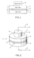
- Figure 1 is a schematic diagram of a bipolar transistor structure in accordance with the present invention.
- Figure 2 is a schematic diagram of a LED structure in accordance with the present invention.
- Figure 3 is a schematic diagram of a laser or light amplifier in accordance with the present invention.
- Figure 4 is a schematic diagram of a structure in accordance with the present invention employing an alternative injection means for the charge carriers.
- a semiconductor substrate 1 such as silicon, germanium, diamond, alloys of such including silicon germanium and silicon carbide, and compound semiconductors including group II-VI such as zinc selenide and related materials, and group III-V such as gallium arsenide and related materials.
- the preferred semiconductor is silicon.
- the semiconductor substrate includes a first p-type or n-type region 2 and a first region 3 of the opposite conductivity type as region 2. In other words, when region 2 is p-type, then region 3 is n-type and vice versa.
- silicon p-type dopants include aluminum, gallium and indium.
- the p-type region is doped with about 1015 to about 1020 and more typically from about 1017 to about 1019 atoms/cm2 dosage.
- N- type dopants for silicon include phosphorous and arsenic.
- Typical dopant concentrations for the n-type dopant are about 1015 to about 1020 and more typical about 1017 to about 1019 atoms/cm2.
- bipolar devices of the present invention include a p-n junction 4. Located in a region in the vicinity of the p-n junction is a region 5 doped with a rare-earth element.
- Suitable rare-earth elements include erbium praseodymium and neodymium, with erbium being preferred.
- the concentration of the rare-earth element is about 1015 to about 1020 such as ion implantation or can be incorporated into the structure during an epitaxial growth.
- the region containing the rare earth element is a reverse biased junction and is the collector of a bipolar transistor.
- Means 6 for injecting charge carriers to one of the p- type and n-type regions and preferably the p-type region to excite atoms of the rare-earth element is provided.
- This means can be a p-n junction coupled to one of the p-type and n-type regions (see Fig. 1).
- the pn- junction providing the charge is referred to as the emitter.
- an electron beam or light can be used for such purpose (see Fig. 4).
- the light emitting rare-earth-doped layer By placing the light emitting rare-earth-doped layer inside the reverse-bias collector junction, the competitive recombination that occurs inside a forward-biased junction is eliminated. Moreover, by having the emitter-base junction present, an independent control of the current density and electrical field is achieved, thereby providing a ready source of carriers with sufficient energy to excite the rare earth element via an impact ionization process.
- Figure 2 illustrates a light emitting diode pursuant to the present invention including a semiconductor substrate 1, a first p-type or n-type region 2 and a first region 3 of the opposite conductivity type as region 2, a p-n junction 4 and a region 5 doped with a rare-earth element.
- a charge source 6 is electrically coupled to region 3.
- Electrical conductors 7, 8 and 9 are provided to regions 2, 3 and 6, respectively.
- Figure 3 illustrates a laser or light amplifier pursuant to the present invention including a semiconductor substrate 1, a first p-type or n-type region 2 and a first region 3 of the opposite conductivity type as region 2, a p- n junction 4 and a region 5 doped with a rare-earth element.
- a charge source 6 is electrically coupled to region 3.
- Electrical conductors 7, 8 and 9 are provided to regions 2, 3 and 6, respectively.
- Figure 4 illustrates a structure employing alternative injection means for the charge carriers pursuant to the present invention including a semiconductor substrate 1, a first p-type or n-type region 2 and a first region 3 of the opposite conductivity type as region 2, a p-n junction 4 and a region 5 doped with a rare-earth element.
- a charge source 10 of electron beam or light source is provided for injecting charge carriers to one of the doped regions 2 or 3.
- Electrical conductors 7 and 8 are provided to regions 2 and 3, respectively.
Landscapes
- Semiconductor Lasers (AREA)
- Led Devices (AREA)
- Luminescent Compositions (AREA)
Applications Claiming Priority (2)
| Application Number | Priority Date | Filing Date | Title |
|---|---|---|---|
| US3045598A | 1998-02-25 | 1998-02-25 | |
| US30455 | 1998-02-25 |
Publications (3)
| Publication Number | Publication Date |
|---|---|
| EP0945938A2 true EP0945938A2 (de) | 1999-09-29 |
| EP0945938A3 EP0945938A3 (de) | 2001-07-25 |
| EP0945938B1 EP0945938B1 (de) | 2005-04-27 |
Family
ID=21854281
Family Applications (1)
| Application Number | Title | Priority Date | Filing Date |
|---|---|---|---|
| EP99301326A Expired - Lifetime EP0945938B1 (de) | 1998-02-25 | 1999-02-23 | Elektrisches Pumpen von mit seltenen Erden dotiertem Silizium für optische Emission |
Country Status (6)
| Country | Link |
|---|---|
| US (1) | US6795468B2 (de) |
| EP (1) | EP0945938B1 (de) |
| JP (1) | JP3079093B2 (de) |
| KR (1) | KR100377716B1 (de) |
| DE (1) | DE69924906T2 (de) |
| TW (1) | TW472421B (de) |
Cited By (1)
| Publication number | Priority date | Publication date | Assignee | Title |
|---|---|---|---|---|
| EP1334822A3 (de) * | 2002-02-06 | 2004-06-30 | Tech Epikos - S.R.L. | Verfahren und Anlage zum Lasergravieren von chalkografischen Platten oder Zylindern |
Families Citing this family (7)
| Publication number | Priority date | Publication date | Assignee | Title |
|---|---|---|---|---|
| KR100384892B1 (ko) * | 2000-12-01 | 2003-05-22 | 한국전자통신연구원 | 에르븀이 도핑된 실리콘나노점의 형성 방법 |
| KR100431760B1 (ko) * | 2001-08-08 | 2004-05-17 | 삼성전기주식회사 | AlGaInN계 반도체 엘이디(LED) 소자 및 그 제조 방법 |
| KR100553317B1 (ko) * | 2004-04-23 | 2006-02-20 | 한국과학기술연구원 | 실리콘 나노선을 이용한 실리콘 광소자 및 이의 제조방법 |
| JP4956916B2 (ja) * | 2005-05-30 | 2012-06-20 | ソニー株式会社 | 発光素子及び発光装置 |
| JP5689832B2 (ja) * | 2012-02-10 | 2015-03-25 | 日本電信電話株式会社 | シリコン発光素子の製造方法 |
| CN102828242B (zh) * | 2012-09-06 | 2015-05-27 | 西安隆基硅材料股份有限公司 | 含有下转换发光量子点的晶体硅及其制备方法 |
| WO2021149235A1 (ja) * | 2020-01-24 | 2021-07-29 | 日本碍子株式会社 | 希土類含有SiC基板及びSiCエピタキシャル層の製法 |
Family Cites Families (15)
| Publication number | Priority date | Publication date | Assignee | Title |
|---|---|---|---|---|
| DE3344138A1 (de) | 1982-12-11 | 1984-06-14 | Fraunhofer-Gesellschaft zur Förderung der angewandten Forschung e.V., 8000 München | Optoelektronisches bauelement, insbesondere eine laserdiode oder eine leuchtdiode |
| JPS6229190A (ja) | 1985-07-30 | 1987-02-07 | Nec Corp | 半導体レ−ザ |
| JPH0636437B2 (ja) | 1986-05-16 | 1994-05-11 | 日本電気株式会社 | 赤外発光ダイオ−ド |
| FR2674697A1 (fr) | 1987-04-03 | 1992-10-02 | Thomson Csf | Laser a semiconducteurs et procede de realisation. |
| US4967251A (en) | 1988-08-12 | 1990-10-30 | Sharp Kabushiki Kaisha | Thin film electroluminescent device containing gadolinium and rare earth elements |
| US5248890A (en) | 1989-05-13 | 1993-09-28 | Forschungszentrum Julich Gmbh | Valance specific lanthanide doped optoelectronic metal fluoride semiconductor device |
| US5311035A (en) | 1989-09-04 | 1994-05-10 | Kabushiki Kaisha Komatsu Seisakusho | Thin film electroluminescence element |
| US5119460A (en) | 1991-04-25 | 1992-06-02 | At&T Bell Laboratories | Erbium-doped planar optical device |
| US5107538A (en) | 1991-06-06 | 1992-04-21 | At&T Bell Laboratories | Optical waveguide system comprising a rare-earth Si-based optical device |
| FR2681737A1 (fr) | 1991-09-24 | 1993-03-26 | Thomson Csf | Source monofrequence de puissance a fibre optique. |
| US5322813A (en) | 1992-08-31 | 1994-06-21 | International Business Machines Corporation | Method of making supersaturated rare earth doped semiconductor layers by chemical vapor deposition |
| US5369657A (en) | 1992-09-15 | 1994-11-29 | Texas Instruments Incorporated | Silicon-based microlaser by doped thin films |
| US5319727A (en) | 1992-12-28 | 1994-06-07 | Honeywell Inc. | Ion-beam deposited, gain enhanced ring resonators |
| DE69323884T2 (de) | 1993-10-20 | 1999-07-22 | Consorzio Per La Ricerca Sulla Microelettronica Nel Mezzogiorno, Catania | Elektrolumineszente Festkörpervorrichtung und Verfahren zu ihrer Herstellung |
| US5530709A (en) | 1994-09-06 | 1996-06-25 | Sdl, Inc. | Double-clad upconversion fiber laser |
-
1999
- 1999-01-29 KR KR10-1999-0002911A patent/KR100377716B1/ko not_active Expired - Fee Related
- 1999-02-01 TW TW088101496A patent/TW472421B/zh not_active IP Right Cessation
- 1999-02-18 JP JP3965899A patent/JP3079093B2/ja not_active Expired - Fee Related
- 1999-02-23 DE DE69924906T patent/DE69924906T2/de not_active Expired - Lifetime
- 1999-02-23 EP EP99301326A patent/EP0945938B1/de not_active Expired - Lifetime
-
2003
- 2003-06-16 US US10/461,919 patent/US6795468B2/en not_active Expired - Fee Related
Cited By (1)
| Publication number | Priority date | Publication date | Assignee | Title |
|---|---|---|---|---|
| EP1334822A3 (de) * | 2002-02-06 | 2004-06-30 | Tech Epikos - S.R.L. | Verfahren und Anlage zum Lasergravieren von chalkografischen Platten oder Zylindern |
Also Published As
| Publication number | Publication date |
|---|---|
| TW472421B (en) | 2002-01-11 |
| JP3079093B2 (ja) | 2000-08-21 |
| US6795468B2 (en) | 2004-09-21 |
| KR100377716B1 (ko) | 2003-03-26 |
| EP0945938B1 (de) | 2005-04-27 |
| EP0945938A3 (de) | 2001-07-25 |
| KR19990072328A (ko) | 1999-09-27 |
| DE69924906T2 (de) | 2006-06-01 |
| US20040037335A1 (en) | 2004-02-26 |
| DE69924906D1 (de) | 2005-06-02 |
| JPH11340504A (ja) | 1999-12-10 |
Similar Documents
| Publication | Publication Date | Title |
|---|---|---|
| US5448082A (en) | Light emitting diode for use as an efficient emitter or detector of light at a common wavelength and method for forming the same | |
| Coffa et al. | Light emission from Er-doped Si: materials properties, mechanisms, and device performance | |
| JP2549723B2 (ja) | シリコンエレクトロルミネセント素子 | |
| US8890177B2 (en) | Semiconductor devices made from crystalline materials with locally modifying electronic and optoelectronic properties | |
| Zandian et al. | HgCdTe double heterostructure injection laser grown by molecular beam epitaxy | |
| EP0261875B1 (de) | Halbleiterlaser mit Dotierung von seltenen Erden | |
| Galtier et al. | 1.54 μm room‐temperature electroluminescence of erbium‐doped GaAs and GaAlAs grown by molecular beam epitaxy | |
| EP0945938B1 (de) | Elektrisches Pumpen von mit seltenen Erden dotiertem Silizium für optische Emission | |
| Weiser et al. | Electroluminescent gallium arsenide diodes with negative resistance | |
| US6828598B1 (en) | Semiconductor device for electro-optic applications, method for manufacturing said device and corresponding semiconductor laser device | |
| KR19990044863A (ko) | 발광 디바이스 | |
| Chang et al. | Studies of GaAs: Er impact excited electroluminescence devices | |
| Lee et al. | High avalanche gain in small‐area InP photodiodes | |
| Chang et al. | 1.54 μm electroluminescence from erbium-doped SiGe light emitting diodes | |
| Bresler et al. | Electroluminescence efficiency of silicon diodes | |
| JPH0636437B2 (ja) | 赤外発光ダイオ−ド | |
| Ni et al. | Device aspects of Er-doped Si structures for optoelectric interconnect applications | |
| JP2929632B2 (ja) | 光素子の製造方法 | |
| Jantsch et al. | Status, Hopes and Limitations for the Si: Er-based 1.54 μm Emitter | |
| Chen et al. | Optoelectronic property of PN junction on erbium-doped silicon using thermal diffusion method | |
| Chang | Neodymium‐doped GaAs light‐emitting diodes | |
| Chang | Neodymium-doped GaAs light-emitting diodes | |
| Ni et al. | SiGe/Si: Er Light Emitting Transistors | |
| L'Haridon et al. | New LED In Synthesized InP Yb Material | |
| Garter et al. | Visible and Infrared Rare-Earth Activated Electroluminescence From Erbium Doped GaN |
Legal Events
| Date | Code | Title | Description |
|---|---|---|---|
| PUAI | Public reference made under article 153(3) epc to a published international application that has entered the european phase |
Free format text: ORIGINAL CODE: 0009012 |
|
| AK | Designated contracting states |
Kind code of ref document: A2 Designated state(s): DE FR GB IE |
|
| AX | Request for extension of the european patent |
Free format text: AL;LT;LV;MK;RO;SI |
|
| PUAL | Search report despatched |
Free format text: ORIGINAL CODE: 0009013 |
|
| AK | Designated contracting states |
Kind code of ref document: A3 Designated state(s): AT BE CH CY DE DK ES FI FR GB GR IE IT LI LU MC NL PT SE |
|
| AX | Request for extension of the european patent |
Free format text: AL;LT;LV;MK;RO;SI |
|
| 17P | Request for examination filed |
Effective date: 20011227 |
|
| AKX | Designation fees paid |
Free format text: DE FR GB IE |
|
| 17Q | First examination report despatched |
Effective date: 20040213 |
|
| GRAP | Despatch of communication of intention to grant a patent |
Free format text: ORIGINAL CODE: EPIDOSNIGR1 |
|
| RIN1 | Information on inventor provided before grant (corrected) |
Inventor name: VARHUE, WALTER J.C/O IBM U.K.LTD. Inventor name: PEKARIK, JOHN J. |
|
| GRAS | Grant fee paid |
Free format text: ORIGINAL CODE: EPIDOSNIGR3 |
|
| GRAA | (expected) grant |
Free format text: ORIGINAL CODE: 0009210 |
|
| AK | Designated contracting states |
Kind code of ref document: B1 Designated state(s): DE FR GB IE |
|
| REG | Reference to a national code |
Ref country code: GB Ref legal event code: FG4D |
|
| RIC1 | Information provided on ipc code assigned before grant |
Ipc: 7H 01L 33/00 A |
|
| REG | Reference to a national code |
Ref country code: IE Ref legal event code: FG4D |
|
| REF | Corresponds to: |
Ref document number: 69924906 Country of ref document: DE Date of ref document: 20050602 Kind code of ref document: P |
|
| PLBE | No opposition filed within time limit |
Free format text: ORIGINAL CODE: 0009261 |
|
| STAA | Information on the status of an ep patent application or granted ep patent |
Free format text: STATUS: NO OPPOSITION FILED WITHIN TIME LIMIT |
|
| ET | Fr: translation filed | ||
| 26N | No opposition filed |
Effective date: 20060130 |
|
| PGFP | Annual fee paid to national office [announced via postgrant information from national office to epo] |
Ref country code: IE Payment date: 20070221 Year of fee payment: 9 |
|
| REG | Reference to a national code |
Ref country code: GB Ref legal event code: 746 Effective date: 20080117 |
|
| REG | Reference to a national code |
Ref country code: IE Ref legal event code: MM4A |
|
| PG25 | Lapsed in a contracting state [announced via postgrant information from national office to epo] |
Ref country code: IE Free format text: LAPSE BECAUSE OF NON-PAYMENT OF DUE FEES Effective date: 20080225 |
|
| PGFP | Annual fee paid to national office [announced via postgrant information from national office to epo] |
Ref country code: FR Payment date: 20110216 Year of fee payment: 13 |
|
| REG | Reference to a national code |
Ref country code: FR Ref legal event code: ST Effective date: 20121031 |
|
| PG25 | Lapsed in a contracting state [announced via postgrant information from national office to epo] |
Ref country code: FR Free format text: LAPSE BECAUSE OF NON-PAYMENT OF DUE FEES Effective date: 20120229 |
|
| PGFP | Annual fee paid to national office [announced via postgrant information from national office to epo] |
Ref country code: GB Payment date: 20170130 Year of fee payment: 19 |
|
| PGFP | Annual fee paid to national office [announced via postgrant information from national office to epo] |
Ref country code: DE Payment date: 20180201 Year of fee payment: 20 |
|
| GBPC | Gb: european patent ceased through non-payment of renewal fee |
Effective date: 20180223 |
|
| REG | Reference to a national code |
Ref country code: DE Ref legal event code: R071 Ref document number: 69924906 Country of ref document: DE |
|
| PG25 | Lapsed in a contracting state [announced via postgrant information from national office to epo] |
Ref country code: GB Free format text: LAPSE BECAUSE OF NON-PAYMENT OF DUE FEES Effective date: 20180223 |