EP0945982A1 - Differentieller Impulsverstärker mit konstantem Tastverhältnis - Google Patents
Differentieller Impulsverstärker mit konstantem Tastverhältnis Download PDFInfo
- Publication number
- EP0945982A1 EP0945982A1 EP99302215A EP99302215A EP0945982A1 EP 0945982 A1 EP0945982 A1 EP 0945982A1 EP 99302215 A EP99302215 A EP 99302215A EP 99302215 A EP99302215 A EP 99302215A EP 0945982 A1 EP0945982 A1 EP 0945982A1
- Authority
- EP
- European Patent Office
- Prior art keywords
- transistors
- amplifier
- pulse amplifier
- input signals
- current
- Prior art date
- Legal status (The legal status is an assumption and is not a legal conclusion. Google has not performed a legal analysis and makes no representation as to the accuracy of the status listed.)
- Granted
Links
- 238000000034 method Methods 0.000 claims description 10
- 230000001934 delay Effects 0.000 claims description 8
- 229920006395 saturated elastomer Polymers 0.000 claims description 3
- 238000013459 approach Methods 0.000 claims description 2
- 230000005669 field effect Effects 0.000 claims 2
- 230000000694 effects Effects 0.000 description 2
- 238000010586 diagram Methods 0.000 description 1
- 238000012986 modification Methods 0.000 description 1
- 230000004048 modification Effects 0.000 description 1
Images

Classifications
-
- H—ELECTRICITY
- H03—ELECTRONIC CIRCUITRY
- H03K—PULSE TECHNIQUE
- H03K5/00—Manipulating of pulses not covered by one of the other main groups of this subclass
- H03K5/22—Circuits having more than one input and one output for comparing pulses or pulse trains with each other according to input signal characteristics, e.g. slope, integral
- H03K5/24—Circuits having more than one input and one output for comparing pulses or pulse trains with each other according to input signal characteristics, e.g. slope, integral the characteristic being amplitude
- H03K5/2472—Circuits having more than one input and one output for comparing pulses or pulse trains with each other according to input signal characteristics, e.g. slope, integral the characteristic being amplitude using field effect transistors
- H03K5/2481—Circuits having more than one input and one output for comparing pulses or pulse trains with each other according to input signal characteristics, e.g. slope, integral the characteristic being amplitude using field effect transistors with at least one differential stage
-
- H—ELECTRICITY
- H03—ELECTRONIC CIRCUITRY
- H03K—PULSE TECHNIQUE
- H03K5/00—Manipulating of pulses not covered by one of the other main groups of this subclass
- H03K5/156—Arrangements in which a continuous pulse train is transformed into a train having a desired pattern
- H03K5/1565—Arrangements in which a continuous pulse train is transformed into a train having a desired pattern the output pulses having a constant duty cycle
Definitions
- the present invention relates to a low power pulse amplifier, and more particularly to a low power pulse amplifier with a low duty cycle error at high input levels.
- the duty cycle requirements for pulse amplifiers of this type excludes the use of single-ended amplifiers since clipping at higher amplitudes results in different clip levels and delays in the positive and negative directions.
- an ordinary differential stage consisting of a differential pair of transistors produces asymmetrical delays in the positive and negative directions of the input signal if the input signal is large.
- the main reason for this is that the common source node for the differential pair will change its potential differently between large positive and large negative input signals.
- An object of the present invention is to provide an improved pulse amplifier.
- a pulse amplifier comprising an input for receiving input signals, an output, and a plurality of fully differential amplifier stages between said input and output arranged to ensure more symmetrical delays in positive and negative directions of the input signals.
- each fully differential amplifier stage comprises first and second transistors forming a differential pair and having a common node, a pair of load transistors in parallel with the respective first and second transistors, and a limiting circuit for limiting the voltage swing of the common node to a substantially constant voltage for large input signals. It is however possible to place the load transistors in series with the transistors of the differential pair.
- the invention also preferably includes a biasing network and an offset canceling network.
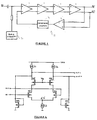
- the pulse amplifier with low duty cycle shown in Figure 1 consists of several cascaded fully differential, i.e. differential in/differential out, amplifier stages 1, a biasing network 2, and an offset canceling network 3 consisting of a low pass filter 4 and an ordinary differential amplifier 5.
- the gain of the amplifier 5 and the cut-off frequency of the low pass filter 4 in the offset canceling network should be chosen so that the resulting high pass characteristic of the canceling network has a cut-off frequency below the frequencies contained in the input signal applied to the amplifier.
- Figure 2 illustrates an amplifier stage 1 with a NMOS input, although it will be understood that the amplifier can be configured in opposite logic using PMOS components.
- Differential input signals IN+, IN-, are applied to respective NMOS transistors M1, M2 having a common node CN and together forming a differential pair.
- Transistors M1, M2 are in series with respective cascode transistors M5, M6 providing respective differential outputs OUT+, OUT-.
- Current sources I 1 , I 2 for the differential pair are connected to supply rail V DD .
- Load transistors M3 and M4 are connected in parallel with respective series combinations Ml, M5 and M2, M6 to the same supply V DD as the current sources I 1 ,I 2 for the differential pair M1, M2 in order to minimize the supply voltage needed to drive the amplifier.
- the two matching current sources I 1 and I 2 are larger than current source I 3 connected to common node CN to guarantee that there is always a current flowing through M3 and M4 even when the differential stage is fully saturated. This reduces the output voltage swing during clipping.
- the gate voltage to the cascode transistors is chosen to set the Vds of the differential pair above, but not substantially above, the saturation voltage of these transistors. The holds true as long as the amplifier circuit is not clipping due to large input signals.
- the cascode transistors ultimately turn off if a large input signal charges the common source node of the differential pair toward the output dc level so this node will be held relatively constant for very large input signals resulting in significantly more symmetric delays in positive and negative directions.
- one of the transistors of the differential pair say M1
- M1 In the presence of large input signals, one of the transistors of the differential pair, say M1, is driven hard into conduction, and its drain in effect gradually becomes shorted to the common node.
- the drain of transistor M1 is connected to the source of transistor M5, and consequently the voltage of the source of cascode transistor M5 approaches the voltage of its gate, so that the current flow through transistor M5 gradually reduces until it eventually turns off. This of course has the effect of gradually reducing the current flow through the associated differential transistor M1.
- the gain is set by the ratio of transconductance in M1 and M3. It is advantageous to use the same type of transistors in both the differential pair and the load to minimize the gain variations due to process spread and the threshold voltage variations. In all normal cases the gain is larger than one, so M3 will have a lower transconductance than M1. With I 1 and I 2 being than I 3 , the dc current in the load transistors M3 and M4 will be larger than in Ml and M2, so W/L for M3 and M4 has to be smaller than in M1 and M2 to move them deeper into strong inversion and lower the transconductance. This results in a larger Vgs for the load transistors than for the differential pair, so there will be enough voltage over the current source for the differential pair to function correctly if the input of one gain stage is dc coupled to the output of the previous stage.
- the bias network generates the bias voltages for the current sources and the cascode transistors. With an ac coupled signal, the bias network also supplies the dc bias for the input node. In cases where the amplifier is powered on and off, the start-up time can be reduced if the offset cancellation feedback signal is held at a voltage near the dc input voltage while the amplifier is disabled.
- the current sources I 1 to I 3 can be implemented as simple current mirrors or cascoded current mirrors if better PSRR (Power Supply Rejection Ratio) is required.
- the offset voltage at the output may be acceptable without offset cancellation.
- the reference input is connected to a fixed voltage instead, typically the same voltage biasing the signal input.
- the circuit can be turned inverted with all NMOS transistors replaced by PMOS transistors and vice versa.
- the amplifiers can also be made variable gain amplifiers if the current source I 3 is made variable. A lower I 3 current will reduce the transconductance in the differential pair and also increase the current in the load transistors and increase their transconductance.
- the cascode transistors may not be needed and can be removed to save space. Even in an amplifier with a single ended input this is true in all but the first stage.
- the NMOS load transistors M3, M4 can be replaced by PMOS transistors with their sources tied to their outputs, the drains to Vss and their gates to a voltage V G , which is approximately the desired output voltage minus a PMOS threshold voltage.
- V G which is approximately the desired output voltage minus a PMOS threshold voltage.
- the pulse amplifier is general in nature and can be used in a wide range of applications. Signals should be ac coupled since the input common mode range is limited. In particular, it can amplify a Manchester coded data stream at 300 kbits/sec. The amplitude ranges from 5 mV pp up to the supply voltage and maintains a duty cycle error of less than 5%.
- the load transistors M3 and M4 can be placed in series with the cascode transistors M5, M6, in which case they change places with the current sources I 1 , I 2 .
Landscapes
- Physics & Mathematics (AREA)
- Nonlinear Science (AREA)
- Amplifiers (AREA)
Applications Claiming Priority (4)
| Application Number | Priority Date | Filing Date | Title |
|---|---|---|---|
| US7966898P | 1998-03-27 | 1998-03-27 | |
| US79668P | 1998-03-27 | ||
| CA002233527A CA2233527C (en) | 1998-03-30 | 1998-03-30 | Pulse amplifier with low-duty cycle errors |
| CA2233527 | 1998-03-30 |
Publications (2)
| Publication Number | Publication Date |
|---|---|
| EP0945982A1 true EP0945982A1 (de) | 1999-09-29 |
| EP0945982B1 EP0945982B1 (de) | 2004-02-11 |
Family
ID=25680113
Family Applications (1)
| Application Number | Title | Priority Date | Filing Date |
|---|---|---|---|
| EP19990302215 Expired - Lifetime EP0945982B1 (de) | 1998-03-27 | 1999-03-23 | Differentieller Impulsverstärker mit konstantem Tastverhältnis |
Country Status (2)
| Country | Link |
|---|---|
| EP (1) | EP0945982B1 (de) |
| DE (1) | DE69914652T2 (de) |
Citations (6)
| Publication number | Priority date | Publication date | Assignee | Title |
|---|---|---|---|---|
| EP0358518A1 (de) * | 1988-09-09 | 1990-03-14 | Honeywell Inc. | 50 Prozent-Präzisionstastverhältnisregler |
| EP0451378A1 (de) * | 1990-04-10 | 1991-10-16 | Hewlett-Packard Limited | FET-Verstärkerschaltungen und Wirkungsmethoden |
| GB2258779A (en) * | 1989-02-08 | 1993-02-17 | Burr Brown Corp | Fet differential amplifier with output offset correction. |
| WO1995022202A1 (en) * | 1994-02-15 | 1995-08-17 | Rambus, Inc. | Amplifier with active duty cycle correction |
| WO1995022206A1 (en) * | 1994-02-15 | 1995-08-17 | Rambus, Inc. | Delay-locked loop |
| US5512848A (en) * | 1994-09-16 | 1996-04-30 | Texas Instruments Incorporated | Offset comparator with common mode voltage stability |
-
1999
- 1999-03-23 EP EP19990302215 patent/EP0945982B1/de not_active Expired - Lifetime
- 1999-03-23 DE DE1999614652 patent/DE69914652T2/de not_active Expired - Fee Related
Patent Citations (6)
| Publication number | Priority date | Publication date | Assignee | Title |
|---|---|---|---|---|
| EP0358518A1 (de) * | 1988-09-09 | 1990-03-14 | Honeywell Inc. | 50 Prozent-Präzisionstastverhältnisregler |
| GB2258779A (en) * | 1989-02-08 | 1993-02-17 | Burr Brown Corp | Fet differential amplifier with output offset correction. |
| EP0451378A1 (de) * | 1990-04-10 | 1991-10-16 | Hewlett-Packard Limited | FET-Verstärkerschaltungen und Wirkungsmethoden |
| WO1995022202A1 (en) * | 1994-02-15 | 1995-08-17 | Rambus, Inc. | Amplifier with active duty cycle correction |
| WO1995022206A1 (en) * | 1994-02-15 | 1995-08-17 | Rambus, Inc. | Delay-locked loop |
| US5512848A (en) * | 1994-09-16 | 1996-04-30 | Texas Instruments Incorporated | Offset comparator with common mode voltage stability |
Also Published As
| Publication number | Publication date |
|---|---|
| DE69914652D1 (de) | 2004-03-18 |
| EP0945982B1 (de) | 2004-02-11 |
| DE69914652T2 (de) | 2004-10-07 |
Similar Documents
| Publication | Publication Date | Title |
|---|---|---|
| EP3437187B1 (de) | System und verfahren zur steuerung der gleichtaktspannung über eine replikaschaltung und rückkopplungsregelung | |
| US6573779B2 (en) | Duty cycle integrator with tracking common mode feedback control | |
| US4554515A (en) | CMOS Operational amplifier | |
| US5754078A (en) | Operational amplifier for class B amplification | |
| US5381114A (en) | Continuous time common mode feedback amplifier | |
| US6208199B1 (en) | Pulse amplifier with low duty cycle errors | |
| US5006817A (en) | Rail-to-rail CMOS operational amplifier | |
| US6891433B2 (en) | Low voltage high gain amplifier circuits | |
| US6731169B2 (en) | Differential amplifier circuit | |
| EP2047593B1 (de) | Stapelpuffer | |
| US7446607B2 (en) | Regulated cascode circuit, an amplifier including the same, and method of regulating a cascode circuit | |
| JPH01106607A (ja) | 増幅回路配置 | |
| KR100313504B1 (ko) | 알티알 입력단의 트랜스컨덕턴스 제어회로 | |
| JP2023505464A (ja) | マルチチャネルマルチプレクサ | |
| US20040239426A1 (en) | Operational amplifier generating desired feedback reference voltage allowing improved output characteristic | |
| US7852159B2 (en) | Method for adaptive biasing of fully differential gain boosted operational amplifiers | |
| US6975100B2 (en) | Circuit arrangement for regulating the duty cycle of electrical signal | |
| CN112468091B (zh) | 放大器偏置技术 | |
| US6525602B1 (en) | Input stage for a buffer with negative feed-back | |
| EP0945982B1 (de) | Differentieller Impulsverstärker mit konstantem Tastverhältnis | |
| JP7025498B2 (ja) | メモリ制御装置及びメモリ制御方法 | |
| JP6949463B2 (ja) | シングル差動変換回路 | |
| US20020005757A1 (en) | Fully differential operational amplifier of the folded cascode type | |
| US11228283B2 (en) | Negative impedance circuit for reducing amplifier noise | |
| JP2002314399A (ja) | 半導体集積回路 |
Legal Events
| Date | Code | Title | Description |
|---|---|---|---|
| PUAI | Public reference made under article 153(3) epc to a published international application that has entered the european phase |
Free format text: ORIGINAL CODE: 0009012 |
|
| AK | Designated contracting states |
Kind code of ref document: A1 Designated state(s): DE FR GB SE |
|
| AX | Request for extension of the european patent |
Free format text: AL;LT;LV;MK;RO;SI |
|
| 17P | Request for examination filed |
Effective date: 20000315 |
|
| AKX | Designation fees paid |
Free format text: DE FR GB SE |
|
| 17Q | First examination report despatched |
Effective date: 20021204 |
|
| GRAP | Despatch of communication of intention to grant a patent |
Free format text: ORIGINAL CODE: EPIDOSNIGR1 |
|
| RAP1 | Party data changed (applicant data changed or rights of an application transferred) |
Owner name: ZARLINK SEMICONDUCTOR AB |
|
| GRAS | Grant fee paid |
Free format text: ORIGINAL CODE: EPIDOSNIGR3 |
|
| GRAA | (expected) grant |
Free format text: ORIGINAL CODE: 0009210 |
|
| AK | Designated contracting states |
Kind code of ref document: B1 Designated state(s): DE FR GB SE |
|
| REG | Reference to a national code |
Ref country code: GB Ref legal event code: FG4D |
|
| REF | Corresponds to: |
Ref document number: 69914652 Country of ref document: DE Date of ref document: 20040318 Kind code of ref document: P |
|
| PG25 | Lapsed in a contracting state [announced via postgrant information from national office to epo] |
Ref country code: SE Free format text: LAPSE BECAUSE OF FAILURE TO SUBMIT A TRANSLATION OF THE DESCRIPTION OR TO PAY THE FEE WITHIN THE PRESCRIBED TIME-LIMIT Effective date: 20040511 |
|
| ET | Fr: translation filed | ||
| PLBE | No opposition filed within time limit |
Free format text: ORIGINAL CODE: 0009261 |
|
| STAA | Information on the status of an ep patent application or granted ep patent |
Free format text: STATUS: NO OPPOSITION FILED WITHIN TIME LIMIT |
|
| 26N | No opposition filed |
Effective date: 20041112 |
|
| PGFP | Annual fee paid to national office [announced via postgrant information from national office to epo] |
Ref country code: DE Payment date: 20080821 Year of fee payment: 10 |
|
| PGFP | Annual fee paid to national office [announced via postgrant information from national office to epo] |
Ref country code: FR Payment date: 20080903 Year of fee payment: 10 |
|
| PGFP | Annual fee paid to national office [announced via postgrant information from national office to epo] |
Ref country code: GB Payment date: 20080820 Year of fee payment: 10 |
|
| GBPC | Gb: european patent ceased through non-payment of renewal fee |
Effective date: 20090323 |
|
| REG | Reference to a national code |
Ref country code: FR Ref legal event code: ST Effective date: 20091130 |
|
| PG25 | Lapsed in a contracting state [announced via postgrant information from national office to epo] |
Ref country code: DE Free format text: LAPSE BECAUSE OF NON-PAYMENT OF DUE FEES Effective date: 20091001 |
|
| PG25 | Lapsed in a contracting state [announced via postgrant information from national office to epo] |
Ref country code: GB Free format text: LAPSE BECAUSE OF NON-PAYMENT OF DUE FEES Effective date: 20090323 Ref country code: FR Free format text: LAPSE BECAUSE OF NON-PAYMENT OF DUE FEES Effective date: 20091123 |