EP0945986A2 - Circuit pompe de charge pour boucle à verrouillage de phase - Google Patents
Circuit pompe de charge pour boucle à verrouillage de phase Download PDFInfo
- Publication number
- EP0945986A2 EP0945986A2 EP99105136A EP99105136A EP0945986A2 EP 0945986 A2 EP0945986 A2 EP 0945986A2 EP 99105136 A EP99105136 A EP 99105136A EP 99105136 A EP99105136 A EP 99105136A EP 0945986 A2 EP0945986 A2 EP 0945986A2
- Authority
- EP
- European Patent Office
- Prior art keywords
- transistor
- transistors
- gate
- constant current
- gates
- Prior art date
- Legal status (The legal status is an assumption and is not a legal conclusion. Google has not performed a legal analysis and makes no representation as to the accuracy of the status listed.)
- Granted
Links
Images


Classifications
-
- H—ELECTRICITY
- H03—ELECTRONIC CIRCUITRY
- H03L—AUTOMATIC CONTROL, STARTING, SYNCHRONISATION OR STABILISATION OF GENERATORS OF ELECTRONIC OSCILLATIONS OR PULSES
- H03L7/00—Automatic control of frequency or phase; Synchronisation
- H03L7/06—Automatic control of frequency or phase; Synchronisation using a reference signal applied to a frequency- or phase-locked loop
- H03L7/08—Details of the phase-locked loop
- H03L7/085—Details of the phase-locked loop concerning mainly the frequency- or phase-detection arrangement including the filtering or amplification of its output signal
- H03L7/089—Details of the phase-locked loop concerning mainly the frequency- or phase-detection arrangement including the filtering or amplification of its output signal the phase or frequency detector generating up-down pulses
- H03L7/0891—Details of the phase-locked loop concerning mainly the frequency- or phase-detection arrangement including the filtering or amplification of its output signal the phase or frequency detector generating up-down pulses the up-down pulses controlling source and sink current generators, e.g. a charge pump
- H03L7/0895—Details of the current generators
- H03L7/0896—Details of the current generators the current generators being controlled by differential up-down pulses
-
- H—ELECTRICITY
- H03—ELECTRONIC CIRCUITRY
- H03L—AUTOMATIC CONTROL, STARTING, SYNCHRONISATION OR STABILISATION OF GENERATORS OF ELECTRONIC OSCILLATIONS OR PULSES
- H03L7/00—Automatic control of frequency or phase; Synchronisation
- H03L7/06—Automatic control of frequency or phase; Synchronisation using a reference signal applied to a frequency- or phase-locked loop
- H03L7/08—Details of the phase-locked loop
- H03L7/085—Details of the phase-locked loop concerning mainly the frequency- or phase-detection arrangement including the filtering or amplification of its output signal
- H03L7/089—Details of the phase-locked loop concerning mainly the frequency- or phase-detection arrangement including the filtering or amplification of its output signal the phase or frequency detector generating up-down pulses
- H03L7/0891—Details of the phase-locked loop concerning mainly the frequency- or phase-detection arrangement including the filtering or amplification of its output signal the phase or frequency detector generating up-down pulses the up-down pulses controlling source and sink current generators, e.g. a charge pump
- H03L7/0893—Details of the phase-locked loop concerning mainly the frequency- or phase-detection arrangement including the filtering or amplification of its output signal the phase or frequency detector generating up-down pulses the up-down pulses controlling source and sink current generators, e.g. a charge pump the up-down pulses controlling at least two source current generators or at least two sink current generators connected to different points in the loop
-
- H—ELECTRICITY
- H03—ELECTRONIC CIRCUITRY
- H03L—AUTOMATIC CONTROL, STARTING, SYNCHRONISATION OR STABILISATION OF GENERATORS OF ELECTRONIC OSCILLATIONS OR PULSES
- H03L7/00—Automatic control of frequency or phase; Synchronisation
- H03L7/06—Automatic control of frequency or phase; Synchronisation using a reference signal applied to a frequency- or phase-locked loop
- H03L7/08—Details of the phase-locked loop
- H03L7/085—Details of the phase-locked loop concerning mainly the frequency- or phase-detection arrangement including the filtering or amplification of its output signal
- H03L7/089—Details of the phase-locked loop concerning mainly the frequency- or phase-detection arrangement including the filtering or amplification of its output signal the phase or frequency detector generating up-down pulses
- H03L7/0891—Details of the phase-locked loop concerning mainly the frequency- or phase-detection arrangement including the filtering or amplification of its output signal the phase or frequency detector generating up-down pulses the up-down pulses controlling source and sink current generators, e.g. a charge pump
- H03L7/0895—Details of the current generators
Definitions
- the present invention relates to a charge pump circuit for a PLL (Phase Locked Loop) and, more particularly, to a charge pump circuit for a PLL used in an integrated circuit requiring functions such as phasing, frequency multiplication, and clock recovery.
- PLL Phase Locked Loop
- CMOS IC Complementary Metal-Oxide Semiconductor Integrated Circuit
- functions such as phasing, frequency multiplication, and clock recovery uses a PLL to control the frequency.
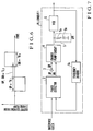
- Fig. 7 shows the basic arrangement of a general PLL.
- a PLL 1 is constituted by a phase detector (PD) 2, an inverter 3, a charge pump circuit 4, a low-pass filter (LPF) 5, a voltage-controlled oscillator (VCO) 6, and a frequency divider 6a.
- PD phase detector
- LPF low-pass filter
- VCO voltage-controlled oscillator
- the PD 2 compares the phases of a reference clock and an output from the frequency divider 6a.
- the PD 2 outputs a pulse (to be referred to as a signal UP) for increasing the frequency.
- the PD 2 outputs a pulse (to be referred to as a signal DN) for decreasing the frequency.
- a signal UP a signal UP inverted by the inverter 3 is used.
- the output of the charge pump circuit 4 is connected to the LPF 5 made up of a resistor 5a and a capacitor 5b.
- the charge pump circuit 4 removes electric charges from the capacitor 5b of the LPF 5 when the charge pump circuit 4 receives the signal DN, and accumulates electric charges in the capacitor 5b of the LPF 5 when the charge pump circuit 4 receives the signal UP .
- a pulse output from the charge pump circuit 4 is converted into a DC analog signal by the LPF 5.
- the VCO 6 receives the analog signal output from the LPF 5 and outputs a constant-frequency signal.
- the frequency divider 6a is formed from a counter, and divides an output from the VCO 6 into N (N: arbitrary natural number) to supply the divided output to the PD 2.
- the PD 2, charge pump circuit 4, VCO 6, and frequency divider 6a form one loop, and this loop controls the phases, i.e., frequencies of two input signals to the PD 2 to be equal to each other.
- the frequency of an output from the VCO 6 is N times the input frequency.
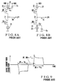
- a power supply VDD is connected to a constant current source 22, and the constant current source 22 is connected to the source of a PMOS transistor 20.
- Ground is connected to a constant current source 23, and the constant current source 23 is connected to the source of an NMOS transistor 21.
- the drains of the PMOS and NMOS transistors 20 and 21 are connected to an LPF on the next stage.
- Fig. 8A schematically shows the case of supplying the signal UP . That is, when the signal UP is at "L" level, the PMOS transistor 20 serving as an analog switch is turned on to supply a current i OH to the LPF.
- a parasitic capacitance Cfp exists between a node C and the power supply VDD.
- the potential of the source side of the PMOS transistor 20 i.e., the potential of the node C changes from the power supply potential to the filter potential, and a current i cfp based on the potential difference and Cfp abruptly flows into the LPF.
- Fig. 8B schematically shows the case of supplying the signal DN. That is, when the signal DN is at "H" level, the NMOS transistor 21 serving as an analog switch is turned on to flow a current i OL from the LPF.
- a parasitic capacitance Cfn exists between a node D and ground.
- the potential of the source side of the NMOS transistor 21, i.e., the potential of the node D changes from ground potential to the filter potential, and a current i cfn based on the potential difference and Cfn abruptly flows from the LPF.
- Fig. 9 shows an output current from the charge pump circuit in Figs. 8A and 8B.
- the currents i cfp and i cfn generate overshoots in an output current from the charge pump circuit to cause jitters in the VCO.
- the phase is permanently repeatedly controlled by an output from the VCO having the jitters, resulting in system errors.
- an overshoot current is the product of the potential difference between the potential of the LPF and the power supply voltage by the magnitude of the parasitic capacitance. For this reason, the overshoot can be eliminated by making the potentials of the nodes C and D equal to the potential of the LPF when the transistors 20 and 21 are in the OFF state.
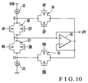
- Fig. 10 shows a conventional charge pump circuit having a function of suppressing an overshoot in an output current.
- CMOS transistors 30 and 31 constituting an analog switch are series-connected between two constant current sources 32 and 33 arranged between the power supply VDD and ground.
- Each of the CMOS transistors 30 and 31 is made up of a parallel circuit of PMOS and NMOS transistors.
- the other terminal of the constant current source 32 having one terminal connected to the power supply VDD is connected to one terminal of a CMOS transistor 34.
- the other terminal of the constant current source 33 having one terminal connected to ground is connected to one terminal of a CMOS transistor 35.
- connection point between the CMOS transistors 30 and 31 is connected to the non-inverting input terminal of an operational amplifier 36 and the LPF.
- the output terminal of the operational amplifier 36 is connected to its inverting input terminal, the other terminal of the CMOS transistor 34, and the other terminal of the CMOS transistor 35.
- the operational amplifier 36 incorporates a phase compensation capacitor (not shown) for preventing oscillation.
- the CMOS transistors 30 and 31 and the CMOS transistors 34 and 35 operate in opposite phases. In other words, while the CMOS transistors 30 and 31 are in the OFF state, the CMOS transistors 34 and 35 are in the ON state.
- the potentials of the nodes E and G are made equal to the potential of the node F (i.e., the potential of the LPF) by feedback at the operational amplifier 36. Even if the CMOS transistors 30 and 31 are turned on, the potentials of the nodes E and G do not change, and no overshoot is generated in an output current.
- the capacitor (not shown) in the operational amplifier 36 has a capacitance of about 6 pF.
- the capacitor occupies a large area with respect to the layout area, which interferes with downsizing the chip.
- a charge pump circuit for a PLL comprising first and second constant current sources for generating constant currents, a first current mirror circuit for supplying a constant current having a value corresponding to the constant current generated by the first constant current source to an output terminal, the first current mirror circuit having a first transistor connected to the first constant current source and a second transistor connected to the output terminal, a second current mirror circuit for supplying a constant current having a value corresponding to the constant current generated by the second constant current source to the output terminal, the second current mirror circuit having a third transistor connected to the second constant current source and a fourth transistor connected to the output terminal, a first analog switch circuit which is connected between gates of the first and second transistors and turned on/off by a first control pulse, and a second analog switch circuit which is connected between gates of the third and fourth transistors and turned on/off by a second control pulse.
- Fig. 1 shows a charge pump circuit for a PLL according to the first embodiment of the present invention.
- the charge pump circuit of the first embodiment is constituted by a first current mirror circuit 21 made up of PMOS transistors 7 and 9, a second current mirror circuit 22 made up of NMOS transistors 12 and 14, constant current sources 10 and 11, and first and second analog switch circuits 8 and 13.
- the PMOS transistor 7 having a source connected to a power supply VDD and a drain connected to the constant current source 10, and the PMOS transistor 9 having a source connected to the power supply VDD constitute the current mirror circuit 21, as described above.
- the first analog switch circuit 8 made up of a CMOS transistor 81 serving as a transfer gate and a PMOS transistor 82 is connected between the gates of the PMOS transistors 7 and 9.
- the CMOS transistor 81 is series-connected between the gates of the PMOS transistors 7 and 9, and the PMOS transistor 82 is connected between the power supply VDD and the gate of the PMOS transistor 9.
- the gate of the CMOS transistor 81 on the PMOS transistor side receives a signal UP
- the gate on the NMOS transistor side receives a signal UP.
- the gate of the PMOS transistor 82 receives the signal UP.
- the NMOS transistor 12 having a source connected to ground and a drain connected to the constant current source 11, and the NMOS transistor 14 having a source connected to ground constitute the second current mirror circuit 22, as described above.
- the CMOS transistor 131 is series-connected between the gates of the NMOS transistors 12 and 14, and the NMOS transistor 132 is connected between the gate of the NMOS transistor 14 and ground.
- the gate of the CMOS transistor 131 on the PMOS transistor side receives a signal DN
- the gate on the NMOS transistor side receives a signal DN.
- the gate of the NMOS transistor 132 receives a signal DN .
- the current mirror circuits 21 and 22 supply constant currents having values corresponding to constant currents generated by the constant current sources 10 and 11 to the LPF via output terminals.
- the MOS transistors 7, 9, 12, 14, 81, 82, 131, and 132 are formed from MOSFETs (Field Effect Transistors).
- both the CMOS transistors 81 and 131 are in the OFF state, both the PMOS and NMOS transistors 82 and 132 are in the ON state, and both the PMOS and NMOS transistors 9 and 14 are in the OFF state. No current is therefore output to the LPF.
- the CMOS transistor 81 When the signal UP is at "H" level, the CMOS transistor 81 is turned on, and the CMOS transistor 131 is turned off.
- the gates of the PMOS transistors 7 and 9 constituting the current mirror circuit 21 are connected to flow a current corresponding to the mirror ratio of the PMOS transistors 7 and 9 to the PMOS transistor 9. The current flows from the power supply VDD to the LPF via the PMOS transistor 9.
- the CMOS transistor 131 When the signal DN is at "H" level, the CMOS transistor 131 is turned on, and the NMOS transistor 132 is turned off.
- the gates of the NMOS transistors 12 and 14 constituting the current mirror circuit 22 are connected to flow a current corresponding to the mirror ratio of the NMOS transistors 12 and 14 through the NMOS transistor 14. The current flows from the LPF to ground via the NMOS transistor 14.
- the potentials on the source sides of the PMOS and NMOS transistors 9 and 14 do not change, and no overshoot is generated in an output current, as shown in Fig. 6.
- Fig. 2 shows a charge pump circuit according to the second embodiment of the present invention.
- the same reference numerals as in Fig. 1 denote the same parts.
- PMOS and NMOS transistors 83 and 133 respectively replace the CMOS transistors 81 and 131.
- both the signals UP and DN are at "L" level
- both the PMOS and NMOS transistors 83 and 133 are in the OFF state
- both PMOS and NMOS transistors 82 and 132 are in the ON state
- both PMOS and NMOS transistors 9 and 14 are in the OFF state. No current is therefore output to the LPF.
- the PMOS transistor 83 When the signal UP is at "H" level, the PMOS transistor 83 is turned on, and the PMOS transistor 82 is turned off.
- the gates of PMOS transistors 7 and 9 constituting a current mirror circuit are connected to flow a current corresponding to the mirror ratio of the PMOS transistors 7 and 9 to the PMOS transistor 9. The current flows from the power supply VDD to the LPF via the PMOS transistor 9.
- the NMOS transistor 133 When the signal DN is at "H" level, the NMOS transistor 133 is turned on, and the NMOS transistor 132 is turned off.
- the gates of NMOS transistors 12 and 14 constituting a current mirror circuit are connected to flow a current corresponding to the mirror ratio of the NMOS transistors 12 and 14 to the NMOS transistor 14. The current flows from the LPF to ground via the NMOS transistor 14.
- the potentials on the source sides of the PMOS and NMOS transistors 9 and 14 do not change, and no overshoot is generated in an output current, as in the first embodiment.
- Fig. 3 shows a charge pump circuit according to the third embodiment of the present invention.
- the same reference numerals as in Fig. 1 denote the same parts.
- NMOS and PMOS transistors 84 and 134 respectively replace the CMOS transistors 81 and 131.
- both the signals UP and DN are at "L" level
- both the NMOS and PMOS transistors 84 and 134 are in the OFF state
- both PMOS and NMOS transistors 82 and 132 are in the ON state
- both PMOS and NMOS transistors 9 and 14 are in the OFF state. No current is therefore output to the LPF.
- the NMOS transistor 84 When the signal UP is at "H" level, the NMOS transistor 84 is turned on, and the PMOS transistor 82 is turned off.
- the gates of PMOS transistors 7 and 9 constituting a current mirror circuit are connected to flow a current corresponding to the mirror ratio of the PMOS transistors 7 and 9 to the PMOS transistor 9. The current flows from the power supply VDD to the LPF via the PMOS transistor 9.
- the PMOS transistor 134 When the signal DN is at "H" level, the PMOS transistor 134 is turned on, and the NMOS transistor 132 is turned off.
- the gates of NMOS transistors 12 and 14 constituting a current mirror circuit are connected to flow a current corresponding to the mirror ratio of the NMOS transistors 12 and 14 to the NMOS transistor 14. The current flows from the LPF to ground via the NMOS transistor 14.
- the potentials on the source sides of the PMOS and NMOS transistors 9 and 14 do not change, and no overshoot is generated in an output current, as in the first embodiment.
- Fig. 4 shows a charge pump circuit according to the fourth embodiment of the present invention.
- the same reference numerals as in Fig. 1 denote the same parts.
- capacitors 85 and 135 are respectively arranged between the gates (nodes A and B in Fig. 4) of PMOS and NMOS transistors 7 and 12 and ground. Operation of the fourth embodiment is the same as in Fig. 1.
- the potentials at the nodes A and B hardly vary.
- the capacitors 85 and 135 used in the fourth embodiment need not be so large in capacitance as the capacitor incorporated in the operational amplifier 36 in Fig. 10, and suffice to be about 1/3 or less.
- the occupation ratio of the capacitor with respect to the layout area on the chip is smaller than in the circuit shown in Fig. 10, and falls within the allowable range for practical use. Note that when these capacitors are arranged on the circuit shown in Fig. 2 or 3 or a circuit (to be described below) shown in Fig. 5, the same effects can be obtained.
- Fig. 5 shows a charge pump circuit according to the fifth embodiment of the present invention.
- the same reference numerals as in Fig. 1 denote the same parts.
- the fifth embodiment adopts dummy transistors 15 and 16 which operate in an opposite phase to the phase for PMOS and NMOS transistors 9 and 14 upon reception of the signals UP and DN.
- the same constant current sources 10 and 11 as in Fig. 1 are arranged, and the dummy transistor 15 formed from a PMOS transistor is connected between the PMOS transistor 9 and the output terminal to the LPF.
- a CMOS transistor 86 is connected between the gate of the dummy transistor 15 and the connection point between the constant current source 10 and a PMOS transistor 7.
- a PMOS transistor is connected between the power supply VDD and the gate of the dummy transistor 15.
- the dummy transistor 16 formed from an NMOS transistor is connected between the NMOS transistor 14 and the output terminal to the LPF.
- a CMOS transistor 136 is connected between the gate of the dummy transistor 16 and the connection point between the power supply VDD and the constant current source 11.
- An NMOS transistor 137 is connected between the gate of the dummy transistor 16 and ground.
- the gate areas of the dummy transistors 15 and 16 are respectively about half the areas of the PMOS and NMOS transistors 9 and 14. Since the dummy transistors 15 and 16 operate by a signal in an opposite phase, field through noise between the PMOS and NMOS transistors 9 and 14 can be reduced.
- a current by a parasitic capacitance generated in the switch can be reduced without using any operational amplifier. Since no phase compensation capacitor need be arranged, the layout area on the chip can be decreased, compared to the conventional charge pump circuit.
Landscapes
- Stabilization Of Oscillater, Synchronisation, Frequency Synthesizers (AREA)
Applications Claiming Priority (2)
| Application Number | Priority Date | Filing Date | Title |
|---|---|---|---|
| JP7978798 | 1998-03-26 | ||
| JP10079787A JPH11274920A (ja) | 1998-03-26 | 1998-03-26 | Pllのチャージポンプ回路 |
Publications (3)
| Publication Number | Publication Date |
|---|---|
| EP0945986A2 true EP0945986A2 (fr) | 1999-09-29 |
| EP0945986A3 EP0945986A3 (fr) | 1999-12-08 |
| EP0945986B1 EP0945986B1 (fr) | 2005-06-08 |
Family
ID=13699935
Family Applications (1)
| Application Number | Title | Priority Date | Filing Date |
|---|---|---|---|
| EP99105136A Expired - Lifetime EP0945986B1 (fr) | 1998-03-26 | 1999-03-26 | Circuit pompe de charge pour boucle à verrouillage de phase |
Country Status (6)
| Country | Link |
|---|---|
| EP (1) | EP0945986B1 (fr) |
| JP (1) | JPH11274920A (fr) |
| KR (1) | KR100499960B1 (fr) |
| CN (1) | CN1132314C (fr) |
| DE (1) | DE69925661T2 (fr) |
| TW (1) | TW569542B (fr) |
Cited By (3)
| Publication number | Priority date | Publication date | Assignee | Title |
|---|---|---|---|---|
| US6590459B2 (en) | 2000-06-06 | 2003-07-08 | Telefonaktiebolaget Lm Ericsson (Publ) | Phase lock circuit |
| WO2016130258A1 (fr) * | 2015-02-09 | 2016-08-18 | Qualcomm Incorporated | Pompe de charge avec polarisation de gâchette de commutation |
| CN107317580A (zh) * | 2017-07-03 | 2017-11-03 | 中国科学院上海高等研究院 | 一种高稳定性振荡器电路及其实现方法 |
Families Citing this family (14)
| Publication number | Priority date | Publication date | Assignee | Title |
|---|---|---|---|---|
| KR100794695B1 (ko) * | 2001-12-29 | 2008-01-14 | 매그나칩 반도체 유한회사 | 차지 펌프 회로 |
| KR100948696B1 (ko) * | 2002-07-12 | 2010-03-22 | 매그나칩 반도체 유한회사 | 차지 펌프 회로 |
| US7151413B2 (en) * | 2004-12-02 | 2006-12-19 | Via Technologies Inc. | Low noise charge pump for PLL-based frequence synthesis |
| US7170322B2 (en) * | 2005-05-28 | 2007-01-30 | Motorola, Inc. | System and method for reducing transient response in a fractional N phase lock loop |
| DE102006018236A1 (de) * | 2006-04-19 | 2007-11-08 | Xignal Technologies Ag | Steuerbare Stromquelle für einen Phasenregelkreis |
| CN101267205B (zh) * | 2008-04-24 | 2011-07-20 | 无锡紫芯集成电路系统有限公司 | 一种电流可调的电荷泵电路 |
| CN101610082B (zh) * | 2009-07-16 | 2011-12-07 | 哈尔滨工业大学 | 应用于锁相环中的源极开关型电荷泵 |
| JP2012009993A (ja) * | 2010-06-23 | 2012-01-12 | Fuji Electric Co Ltd | チャージポンプ回路 |
| KR101401776B1 (ko) * | 2012-10-08 | 2014-06-02 | 강원대학교산학협력단 | Led 구동 장치 |
| CN103887966B (zh) * | 2014-03-24 | 2017-06-20 | 华为技术有限公司 | 电荷泵的实现电路 |
| CN103957004A (zh) * | 2014-04-16 | 2014-07-30 | 中科芯集成电路股份有限公司 | 一种应用于直接发射机的锁相环环路滤波器电路 |
| JP6736339B2 (ja) * | 2016-04-19 | 2020-08-05 | ザインエレクトロニクス株式会社 | Pll周波数シンセサイザ |
| CN110663186B (zh) | 2017-05-24 | 2022-10-04 | 哉英电子股份有限公司 | Pll频率合成器 |
| JP2023069649A (ja) * | 2021-11-08 | 2023-05-18 | ザインエレクトロニクス株式会社 | 位相補間回路 |
Family Cites Families (6)
| Publication number | Priority date | Publication date | Assignee | Title |
|---|---|---|---|---|
| GB8329511D0 (en) * | 1983-11-04 | 1983-12-07 | Inmos Ltd | Timing apparatus |
| US4792705A (en) * | 1986-03-14 | 1988-12-20 | Western Digital Corporation | Fast switching charge pump |
| US5164889A (en) * | 1991-10-10 | 1992-11-17 | Samsung Semiconductor, Inc. | Gate multiplexed low noise charge pump |
| US5473283A (en) * | 1994-11-07 | 1995-12-05 | National Semiconductor Corporation | Cascode switched charge pump circuit |
| JP3407493B2 (ja) * | 1995-08-22 | 2003-05-19 | 三菱電機株式会社 | チャージポンプ回路およびpll回路 |
| US5818287A (en) * | 1996-06-20 | 1998-10-06 | Ati Technologies Inc. | Gate-switching charge-pump implemented inside a phase locked loop |
-
1998
- 1998-03-26 JP JP10079787A patent/JPH11274920A/ja active Pending
-
1999
- 1999-03-17 TW TW088104120A patent/TW569542B/zh not_active IP Right Cessation
- 1999-03-25 KR KR10-1999-0010236A patent/KR100499960B1/ko not_active Expired - Fee Related
- 1999-03-26 EP EP99105136A patent/EP0945986B1/fr not_active Expired - Lifetime
- 1999-03-26 DE DE69925661T patent/DE69925661T2/de not_active Expired - Fee Related
- 1999-03-26 CN CN99104400A patent/CN1132314C/zh not_active Expired - Fee Related
Cited By (4)
| Publication number | Priority date | Publication date | Assignee | Title |
|---|---|---|---|---|
| US6590459B2 (en) | 2000-06-06 | 2003-07-08 | Telefonaktiebolaget Lm Ericsson (Publ) | Phase lock circuit |
| WO2016130258A1 (fr) * | 2015-02-09 | 2016-08-18 | Qualcomm Incorporated | Pompe de charge avec polarisation de gâchette de commutation |
| US9490696B2 (en) | 2015-02-09 | 2016-11-08 | Qualcomm Incorporated | Charge pump with switching gate bias |
| CN107317580A (zh) * | 2017-07-03 | 2017-11-03 | 中国科学院上海高等研究院 | 一种高稳定性振荡器电路及其实现方法 |
Also Published As
| Publication number | Publication date |
|---|---|
| KR19990078246A (ko) | 1999-10-25 |
| TW569542B (en) | 2004-01-01 |
| EP0945986B1 (fr) | 2005-06-08 |
| CN1132314C (zh) | 2003-12-24 |
| KR100499960B1 (ko) | 2005-07-11 |
| DE69925661T2 (de) | 2006-03-16 |
| JPH11274920A (ja) | 1999-10-08 |
| EP0945986A3 (fr) | 1999-12-08 |
| DE69925661D1 (de) | 2005-07-14 |
| CN1236225A (zh) | 1999-11-24 |
Similar Documents
| Publication | Publication Date | Title |
|---|---|---|
| US6255872B1 (en) | Charge pump circuit for PLL | |
| KR100348198B1 (ko) | 동작 전압의 증가 없이 위상 오프셋을 감소시킬 수 있는위상 동기 루프 회로 | |
| US8558592B2 (en) | Charge pump and active filter for a feedback circuit | |
| EP0945986B1 (fr) | Circuit pompe de charge pour boucle à verrouillage de phase | |
| US6954090B2 (en) | Charge pump having reduced switching noise | |
| JP2002111449A (ja) | 電圧制御発振回路およびそれを備える位相同期ループ回路 | |
| JP4282792B2 (ja) | 出力段、チャージポンプ、復調器及び無線電話デバイス | |
| JP3388071B2 (ja) | 位相同期回路、および位相同期回路を含む半導体装置 | |
| EP1351396B1 (fr) | Boucle à verrouillage de phase avec pompe de charge | |
| US6717446B1 (en) | High speed programmable charge-pump with low charge injection | |
| US20060132208A1 (en) | Controllable idle time current mirror circuit for switching regulators, phase-locked loops, and delay-locked loops | |
| US6320458B1 (en) | Integrated structure with an analog unit supplied by an external supply voltage by means of a low-pass filter and driving elements | |
| US6677789B1 (en) | Rail-to-rail linear charge pump | |
| US20070075755A1 (en) | Smart charge-pump circuit for phase-locked loops | |
| US20100026397A1 (en) | Pll circuit | |
| US7190231B2 (en) | High-performance charge-pump circuit for phase-locked loops | |
| US7162001B2 (en) | Charge pump with transient current correction | |
| KR100970916B1 (ko) | 위상 동기 루프의 루프-필터의 튜닝 | |
| JP4635914B2 (ja) | Pll回路 | |
| JP3081718B2 (ja) | Pll回路 | |
| US7248121B2 (en) | Variable lock-in circuit for phase-locked loops | |
| KR19990079930A (ko) | 위상 동기 루프 회로의 전압 제어 발진기 | |
| KR19990035456A (ko) | 위상고정루프회로 | |
| HK1091963B (en) | Method and device of automatically tuning a loop-filter of a phase locked loop |
Legal Events
| Date | Code | Title | Description |
|---|---|---|---|
| PUAI | Public reference made under article 153(3) epc to a published international application that has entered the european phase |
Free format text: ORIGINAL CODE: 0009012 |
|
| AK | Designated contracting states |
Kind code of ref document: A2 Designated state(s): DE FR GB NL |
|
| AX | Request for extension of the european patent |
Free format text: AL;LT;LV;MK;RO;SI |
|
| PUAL | Search report despatched |
Free format text: ORIGINAL CODE: 0009013 |
|
| AK | Designated contracting states |
Kind code of ref document: A3 Designated state(s): AT BE CH CY DE DK ES FI FR GB GR IE IT LI LU MC NL PT SE |
|
| AX | Request for extension of the european patent |
Free format text: AL;LT;LV;MK;RO;SI |
|
| RIC1 | Information provided on ipc code assigned before grant |
Free format text: 6H 03L 7/089 A, 6H 03K 17/687 B |
|
| 17P | Request for examination filed |
Effective date: 20000406 |
|
| AKX | Designation fees paid |
Free format text: DE FR GB NL |
|
| R17P | Request for examination filed (corrected) |
Effective date: 20000406 |
|
| 17Q | First examination report despatched |
Effective date: 20030306 |
|
| RAP1 | Party data changed (applicant data changed or rights of an application transferred) |
Owner name: NEC ELECTRONICS CORPORATION |
|
| GRAP | Despatch of communication of intention to grant a patent |
Free format text: ORIGINAL CODE: EPIDOSNIGR1 |
|
| GRAS | Grant fee paid |
Free format text: ORIGINAL CODE: EPIDOSNIGR3 |
|
| GRAA | (expected) grant |
Free format text: ORIGINAL CODE: 0009210 |
|
| AK | Designated contracting states |
Kind code of ref document: B1 Designated state(s): DE FR GB NL |
|
| REG | Reference to a national code |
Ref country code: GB Ref legal event code: FG4D |
|
| REF | Corresponds to: |
Ref document number: 69925661 Country of ref document: DE Date of ref document: 20050714 Kind code of ref document: P |
|
| ET | Fr: translation filed | ||
| PLBE | No opposition filed within time limit |
Free format text: ORIGINAL CODE: 0009261 |
|
| STAA | Information on the status of an ep patent application or granted ep patent |
Free format text: STATUS: NO OPPOSITION FILED WITHIN TIME LIMIT |
|
| 26N | No opposition filed |
Effective date: 20060309 |
|
| PGFP | Annual fee paid to national office [announced via postgrant information from national office to epo] |
Ref country code: NL Payment date: 20070315 Year of fee payment: 9 |
|
| PGFP | Annual fee paid to national office [announced via postgrant information from national office to epo] |
Ref country code: GB Payment date: 20070321 Year of fee payment: 9 |
|
| PGFP | Annual fee paid to national office [announced via postgrant information from national office to epo] |
Ref country code: DE Payment date: 20070322 Year of fee payment: 9 |
|
| PGFP | Annual fee paid to national office [announced via postgrant information from national office to epo] |
Ref country code: FR Payment date: 20070308 Year of fee payment: 9 |
|
| GBPC | Gb: european patent ceased through non-payment of renewal fee |
Effective date: 20080326 |
|
| PG25 | Lapsed in a contracting state [announced via postgrant information from national office to epo] |
Ref country code: NL Free format text: LAPSE BECAUSE OF NON-PAYMENT OF DUE FEES Effective date: 20081001 |
|
| NLV4 | Nl: lapsed or anulled due to non-payment of the annual fee |
Effective date: 20081001 |
|
| REG | Reference to a national code |
Ref country code: FR Ref legal event code: ST Effective date: 20081125 |
|
| PG25 | Lapsed in a contracting state [announced via postgrant information from national office to epo] |
Ref country code: DE Free format text: LAPSE BECAUSE OF NON-PAYMENT OF DUE FEES Effective date: 20081001 |
|
| PG25 | Lapsed in a contracting state [announced via postgrant information from national office to epo] |
Ref country code: FR Free format text: LAPSE BECAUSE OF NON-PAYMENT OF DUE FEES Effective date: 20080331 |
|
| PG25 | Lapsed in a contracting state [announced via postgrant information from national office to epo] |
Ref country code: GB Free format text: LAPSE BECAUSE OF NON-PAYMENT OF DUE FEES Effective date: 20080326 |