EP0945998B1 - Récepteur de signaux à haute fréquence avec deux ou plus branches de réception - Google Patents
Récepteur de signaux à haute fréquence avec deux ou plus branches de réception Download PDFInfo
- Publication number
- EP0945998B1 EP0945998B1 EP99105872A EP99105872A EP0945998B1 EP 0945998 B1 EP0945998 B1 EP 0945998B1 EP 99105872 A EP99105872 A EP 99105872A EP 99105872 A EP99105872 A EP 99105872A EP 0945998 B1 EP0945998 B1 EP 0945998B1
- Authority
- EP
- European Patent Office
- Prior art keywords
- input signal
- receive path
- different
- intermediate frequency
- seb
- Prior art date
- Legal status (The legal status is an assumption and is not a legal conclusion. Google has not performed a legal analysis and makes no representation as to the accuracy of the status listed.)
- Expired - Lifetime
Links
- 230000005540 biological transmission Effects 0.000 claims description 7
- 238000006243 chemical reaction Methods 0.000 claims description 6
- 238000001514 detection method Methods 0.000 claims description 6
- 238000005070 sampling Methods 0.000 description 7
- 238000010586 diagram Methods 0.000 description 3
- 230000001629 suppression Effects 0.000 description 3
- 230000036039 immunity Effects 0.000 description 2
- 230000007246 mechanism Effects 0.000 description 2
- 230000001419 dependent effect Effects 0.000 description 1
- 230000000694 effects Effects 0.000 description 1
- 230000008030 elimination Effects 0.000 description 1
- 238000003379 elimination reaction Methods 0.000 description 1
- 238000011156 evaluation Methods 0.000 description 1
- 238000005562 fading Methods 0.000 description 1
- 238000001914 filtration Methods 0.000 description 1
- 230000002452 interceptive effect Effects 0.000 description 1
- 239000000203 mixture Substances 0.000 description 1
- 238000011144 upstream manufacturing Methods 0.000 description 1
Images
Classifications
-
- H—ELECTRICITY
- H04—ELECTRIC COMMUNICATION TECHNIQUE
- H04B—TRANSMISSION
- H04B7/00—Radio transmission systems, i.e. using radiation field
- H04B7/02—Diversity systems; Multi-antenna system, i.e. transmission or reception using multiple antennas
- H04B7/04—Diversity systems; Multi-antenna system, i.e. transmission or reception using multiple antennas using two or more spaced independent antennas
- H04B7/08—Diversity systems; Multi-antenna system, i.e. transmission or reception using multiple antennas using two or more spaced independent antennas at the receiving station
- H04B7/0837—Diversity systems; Multi-antenna system, i.e. transmission or reception using multiple antennas using two or more spaced independent antennas at the receiving station using pre-detection combining
- H04B7/084—Equal gain combining, only phase adjustments
-
- H—ELECTRICITY
- H03—ELECTRONIC CIRCUITRY
- H03D—DEMODULATION OR TRANSFERENCE OF MODULATION FROM ONE CARRIER TO ANOTHER
- H03D7/00—Transference of modulation from one carrier to another, e.g. frequency-changing
- H03D7/16—Multiple-frequency-changing
- H03D7/161—Multiple-frequency-changing all the frequency changers being connected in cascade
-
- H—ELECTRICITY
- H03—ELECTRONIC CIRCUITRY
- H03D—DEMODULATION OR TRANSFERENCE OF MODULATION FROM ONE CARRIER TO ANOTHER
- H03D7/00—Transference of modulation from one carrier to another, e.g. frequency-changing
- H03D7/16—Multiple-frequency-changing
- H03D7/165—Multiple-frequency-changing at least two frequency changers being located in different paths, e.g. in two paths with carriers in quadrature
-
- H—ELECTRICITY
- H03—ELECTRONIC CIRCUITRY
- H03D—DEMODULATION OR TRANSFERENCE OF MODULATION FROM ONE CARRIER TO ANOTHER
- H03D7/00—Transference of modulation from one carrier to another, e.g. frequency-changing
- H03D7/18—Modifications of frequency-changers for eliminating image frequencies
Definitions
- the invention relates to a receiver for high-frequency signals with two or more receiving paths whose output signals are fed to an evaluating detector.
- the carrier frequency When receiving a high-frequency useful signal, the carrier frequency is generally mixed to an intermediate frequency or at higher quality receivers, such a mixture is at least twice with accordingly two intermediate frequency stages.
- the carrier frequency of the input signal is generally converted to a lower frequency position or to the baseband and then fed to a detector. Due to the non-ideal conversion stages used, such as mixers, sample and hold circuits, comparators, analog / digital converters, etc., or due to the receiver structure used unwanted high-frequency signals are converted to other carrier frequencies in the same lower frequency position as the high-frequency useful signal, wherein they superimpose the useful signal in the detector and thus lead to a faulty evaluation of the useful signal. A typical example of this is the image frequencies, but there are also other interference mechanisms that can be eliminated or eliminated by taking appropriate measures.
- EP 0 823 790 A2 discloses a dual-band mobile station in which a RF signal with two frequency bands received via a common antenna is supplied in a frequency-dependent manner to respectively assigned receivers.
- the object is achieved with a receiver of the type mentioned, in which according to the invention at least two receiving paths have different non-linear transmission behavior.
- each reception path has at least one mixing stage for converting an input signal into an intermediate frequency position
- at least two reception paths having different intermediate frequencies are provided.
- each reception path can also be a first mixing stage for mixing to have different first intermediate frequencies and a second mixing stage for mixing to the same second intermediate frequencies, since the use of equal second intermediate frequencies, the processing in the evaluating detector can be simpler.
- the analog / digital converters have different sampling frequencies in at least two receiving paths. Since the unwanted mixing products, which arise as harmonics of the sampling frequency and harmonics of an unwanted signal in analog / digital converters, occur for almost all input frequencies of the unwanted signal with different output frequencies at the analog / digital converters, the superposition of the useful signal is only in maximum to expect a path and the other paths, the detection is possible.
- the analog / digital converters can also be provided in a receiver whose receiving paths contain analog / digital converters that the analog / digital converters have different transducer characteristics in at least two receiving paths. For example, if a quadratic nonlinearity transducer and the other transducer are dominated by a cubic nonlinearity, these different nonlinearities will result in different spurious frequencies that can be eliminated by jointly detecting the two output signals of the receive paths.
- the input signals of all paths are the same, i. H. They reach, for example, from a single antenna in the same way to each receiving path.
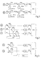
- a receiver with two receiving paths A and B is present, these paths each being supplied with the same input signal sea and seb, e.g. B. a useful signal carrier of 1 GHz.
- This input signal is converted in a mixer M1A or in a mixer M1B firstly by local oscillators L1A with 800 MHz and L1B with 700 MHz to a first intermediate frequency of 200 MHz in path A or to a first intermediate frequency of 300 MHz in path B.
- the second mixers M2A and M2B are each followed by a low-pass filter TPA or TPB, which in this exemplary embodiment has a cut-off frequency of approximately 10 MHz, can be produced with little effort and attenuates the unwanted signals.
- the output signals asa and asb of the two paths A and B are ultimately fed to an evaluating detector ADE, which takes into account the different positions of the signals in the common detection.
- the table shows the frequencies of the different signals according to FIG. 1 in MHz.
- the desired input signal of 1000 MHz leads to the useful signal at the output, whereas the remaining six specified frequencies of the input signal only ever lead in one path to a fault.
- FIG. 2 uses three paths A, B, and C, and each of the paths provides an analog-to-digital converter ADA, ADB, and ADC, these analog-to-digital converters having sampling frequencies f AA , f AB, and f Working AC , which come from a clock generator TAG.
- the input signals of the individual paths A, B and C are here denoted by sea, seb and sec and are also in this case all the same, ie traceable to a common input signal se.
- the sampling frequencies f AA , f AB and f AC are different, so that the unwanted mixing products, which arise in the analog / digital converters of harmonics of the sampling frequency and harmonics of an unwanted signal, for almost all input frequencies of the unwanted signal with different output frequencies to the analog / Digital converters occur.
- the superposition of the useful signal is therefore to be expected only in at most one of the paths A, B and C, whereas the detection in the downstream detector ADE is possible via the other paths.
- the third embodiment of Fig. 3 uses in two receiving paths A and B each an analog / digital converter ADA and ADB, wherein each of the analog / digital converters with the same frequency f T is controlled by a clock generator TAG with respect to its sampling.
- the analog / digital converters ADA and ADB are different in that they have different transducer characteristics.
- the converter ADA can now be equipped with a quadratic converter characteristic, whereas the converter ADB of the path B has a cubic nonlinearity.
Landscapes
- Engineering & Computer Science (AREA)
- Computer Networks & Wireless Communication (AREA)
- Signal Processing (AREA)
- Noise Elimination (AREA)
- Superheterodyne Receivers (AREA)
- Reduction Or Emphasis Of Bandwidth Of Signals (AREA)
- Digital Transmission Methods That Use Modulated Carrier Waves (AREA)
Claims (7)
- Récepteur pour des signaux à haute fréquence comprenant deux chemins de réception ou plus (A, B, C), auxquels est amené le même signal d'entrée (sea, seb, sec), et dont les signaux de sortie (asa, asb, asc) sont amenés à un détecteur d'analyse (ADE) pour la détection commune,
caractérisé en ce que,- pour l'amélioration de la résistance au brouillage, au moins deux chemins de réception (A, B, C) présentent un comportement à la transmission prédéfini, différent et non linéaire,- le comportement à la transmission étant formé par le fait que, dans chaque chemin de réception (A, B), on a dans une première étape une conversion du signal d'entrée (sea, seb) en une première fréquence intermédiaire (ZF1A, ZF1B), qui est choisie différente pour chaque chemin de réception (A, B) et dans une seconde étape le signal d'entrée converti est converti dans une fréquence intermédiaire identique pour tous les chemins de réception (A, B). - Récepteur selon la revendication 1, caractérisé en ce que,- un premier chemin de réception (A) présente un premier niveau de mélange (M1A) pour la conversion du signal d'entrée (sea, seb) en une fréquence intermédiaire (ZF1A),- en ce qu'un second chemin de réception (B) présente un premier niveau de mélange (M1B) pour la conversion du signal d'entrée (sea, seb) en une fréquence intermédiaire (ZF1B), et- en ce que la fréquence intermédiaire (ZF1A) du premier chemin de réception (A) et la fréquence intermédiaire (ZF1B) du second chemin de réception (B) sont choisies différentes.
- Récepteur selon la revendication 1, caractérisé en ce que,- le premier chemin de réception (A) présente un second niveau de mélange (M2A), avec lequel le signal d'entrée (sea, seb) converti à la fréquence intermédiaire (ZF1A) du premier chemin de réception (A) est converti en une seconde fréquence intermédiaire (ZF2A, ZF2B), et- en ce que le second chemin de réception (B) présente un second niveau de mélange (M2B), avec lequel le signal d'entrée (sea, seb) converti à la fréquence intermédiaire (ZF1B) du second chemin de réception (B) est converti dans la seconde fréquence intermédiaire (ZF2A, ZF2B) identique.
- Récepteur pour des signaux à haute fréquence comprenant deux chemins de réception (A, B, C) ou plus, auxquels le même signal d'entrée (sea, seb, sec) est amené, et dont les signaux d'entrée (asa, asb, asc) sont amenés à un détecteur d'analyse (ADE) pour la détection commune,
caractérisé en ce que,- pour l'amélioration de la résistance au brouillage, au moins deux chemins de réception (A, B, C) présentent un comportement à la transmission prédéfini, différent et non linéaire,- le comportement à la transmission étant formé par le fait que, dans chaque chemin de réception (A, B, C), on a une conversion analogique/numérique avec un balayage du signal d'entrée (sea, seb, sec) et on utilise pour chaque chemin de réception (A, B, C) différentes fréquences de balayage (fAA, fAB, fAC). - Récepteur selon la revendication 4, caractérisé en ce que,- chaque chemin de réception (A, B, C) contient un convertisseur analogique/numérique (ADA, ADB, ADC), sur lequel arrive le signal d'entrée pour la conversion analogique/numérique et le balayage, et- en ce que les convertisseurs analogique/numérique (ADA, ADB, ADC) d'au moins deux chemins de réception (A, B, C) présentent différentes fréquences de balayage (fAA, fAB, fAC).
- Récepteur pour des signaux à haute fréquence comprenant deux chemins de réception (A, B, C) ou plus, auxquels le même signal d'entrée (sea, seb, sec) est amené, et dont les signaux d'entrée (asa, asb, asc) sont amenés à un détecteur d'analyse (ADE) pour la détection commune,
caractérisé en ce que,- pour l'amélioration de la résistance au brouillage, au moins deux chemins de réception (A, B, C) présentent un comportement à la transmission prédéfini, différent et non linéaire,- le comportement à la transmission étant formé par le fait que, dans chaque chemin de réception (A, B, C), on a une conversion analogique/numérique du signal d'entrée et la conversion analogique/numérique étant effectuée avec différentes courbes caractéristiques de convertisseur dans chaque chemin de réception (A, B, C). - Récepteur selon la revendication 6, caractérisé en ce que- chaque chemin de réception (A, B) contient un convertisseur analogique/numérique (ADA, ADB), et- en ce que les convertisseurs analogique/numérique (ADA, ADB) d'au moins deux chemins de réception (A, B) présentent différentes courbes caractéristiques de convertisseur.
Applications Claiming Priority (2)
| Application Number | Priority Date | Filing Date | Title |
|---|---|---|---|
| DE19813501 | 1998-03-26 | ||
| DE19813501 | 1998-03-26 |
Publications (3)
| Publication Number | Publication Date |
|---|---|
| EP0945998A2 EP0945998A2 (fr) | 1999-09-29 |
| EP0945998A3 EP0945998A3 (fr) | 2003-10-01 |
| EP0945998B1 true EP0945998B1 (fr) | 2006-06-07 |
Family
ID=7862506
Family Applications (1)
| Application Number | Title | Priority Date | Filing Date |
|---|---|---|---|
| EP99105872A Expired - Lifetime EP0945998B1 (fr) | 1998-03-26 | 1999-03-23 | Récepteur de signaux à haute fréquence avec deux ou plus branches de réception |
Country Status (2)
| Country | Link |
|---|---|
| EP (1) | EP0945998B1 (fr) |
| DE (1) | DE59913498D1 (fr) |
Families Citing this family (1)
| Publication number | Priority date | Publication date | Assignee | Title |
|---|---|---|---|---|
| US9337878B2 (en) * | 2013-12-16 | 2016-05-10 | Motorola Solutions, Inc. | Dual watch radio frequency receiver |
Citations (1)
| Publication number | Priority date | Publication date | Assignee | Title |
|---|---|---|---|---|
| EP0823790A2 (fr) * | 1996-08-07 | 1998-02-11 | Nokia Mobile Phones Ltd. | Station mobile à deux bandes avec des connexions croisées de circuits émetteurs et récepteurs |
Family Cites Families (2)
| Publication number | Priority date | Publication date | Assignee | Title |
|---|---|---|---|---|
| CA1112300A (fr) * | 1978-01-23 | 1981-11-10 | Gerald J.P. Lo | Circuit et methode de reduction de la diaphonie de polarisation due a la pluie |
| GB8519545D0 (en) * | 1985-08-02 | 1985-09-11 | Mcgeehan J P | Transmitters receivers & systems |
-
1999
- 1999-03-23 DE DE59913498T patent/DE59913498D1/de not_active Expired - Fee Related
- 1999-03-23 EP EP99105872A patent/EP0945998B1/fr not_active Expired - Lifetime
Patent Citations (1)
| Publication number | Priority date | Publication date | Assignee | Title |
|---|---|---|---|---|
| EP0823790A2 (fr) * | 1996-08-07 | 1998-02-11 | Nokia Mobile Phones Ltd. | Station mobile à deux bandes avec des connexions croisées de circuits émetteurs et récepteurs |
Also Published As
| Publication number | Publication date |
|---|---|
| EP0945998A3 (fr) | 2003-10-01 |
| DE59913498D1 (de) | 2006-07-20 |
| EP0945998A2 (fr) | 1999-09-29 |
Similar Documents
| Publication | Publication Date | Title |
|---|---|---|
| DE2651300A1 (de) | Kanalwaehler | |
| EP1978647A2 (fr) | Système de réception à large bande | |
| DE69834211T2 (de) | Vorrichtung und verfahren zur verminderung der amplitude von signalen | |
| EP0270188B1 (fr) | Installation de diversité de signal pour la réception mobile | |
| DE69224581T2 (de) | Verstellbare Bandbreite eines Funktelefons | |
| DE69616201T2 (de) | Verbesserungen an oder in bezug auf kommunikationsempfänger | |
| DE112020002240T5 (de) | Verfahren zur Verbesserung der Leistung eines Empfängers mit niedriger Zwischenfrequenz, Speichermedium und Empfänger | |
| DE1441817B2 (de) | Überlagerungsempfänger | |
| DE3600280A1 (de) | Kombinierte mehrfach-empfangsvorrichtung | |
| DE19952249A1 (de) | Aufwärts/Abwärts-Wandler | |
| DE3447282A1 (de) | Funkempfaenger | |
| DE102021209433A1 (de) | Signalempfänger, der Digitalbildsignaltrennung umfasst | |
| DE69823736T2 (de) | Interferenzunterdrückung für HF-Signale | |
| DE3015680C2 (de) | Schaltungsanordnung für einen VHF/UHF-Breitband-Doppelüberlagerungsempfänger in Mikrostreifenleitungstechnik | |
| EP0889646A2 (fr) | Récepteur de signal de télévision | |
| EP0945998B1 (fr) | Récepteur de signaux à haute fréquence avec deux ou plus branches de réception | |
| DE102008012127A1 (de) | Breitband-Empfangssystem | |
| DE69518624T2 (de) | Verbesserungen einen null-zwischenfrequenz-empfänger betreffend | |
| DE69528503T2 (de) | Breitband diskriminator eines funkempfängers | |
| DE202007009431U1 (de) | Breitband-Empfangssystem | |
| EP0552727B1 (fr) | Circuit pour supprimer les signaux d'interférence dans un récepteur d'un système de radiotransmission | |
| EP0185414B1 (fr) | Récepteur FM stéréophonique | |
| DE69519266T2 (de) | Mikrowellenmischerschaltung und diese Schaltung enthaltender Abwärtsumsetzer | |
| DE2713318C2 (de) | Frequenzumsetzer für den Rundfunk- und Fernsehbereich | |
| DE102005013497A1 (de) | Steuerbare Frequenzteilerschaltung, Sende-Empfänger mit steuerbarer Frequenzteilerschaltung und Verfahren zur Durchführung eines Loop-Back-Tests |
Legal Events
| Date | Code | Title | Description |
|---|---|---|---|
| PUAI | Public reference made under article 153(3) epc to a published international application that has entered the european phase |
Free format text: ORIGINAL CODE: 0009012 |
|
| AK | Designated contracting states |
Kind code of ref document: A2 Designated state(s): AT BE CH CY DE DK ES FI FR GB GR IE IT LI LU MC NL PT SE |
|
| AX | Request for extension of the european patent |
Free format text: AL;LT;LV;MK;RO;SI |
|
| PUAL | Search report despatched |
Free format text: ORIGINAL CODE: 0009013 |
|
| AK | Designated contracting states |
Kind code of ref document: A3 Designated state(s): AT BE CH CY DE DK ES FI FR GB GR IE IT LI LU MC NL PT SE |
|
| AX | Request for extension of the european patent |
Extension state: AL LT LV MK RO SI |
|
| RIC1 | Information provided on ipc code assigned before grant |
Ipc: 7H 04B 1/68 B Ipc: 7H 04B 7/08 A |
|
| 17P | Request for examination filed |
Effective date: 20031103 |
|
| 17Q | First examination report despatched |
Effective date: 20040203 |
|
| AKX | Designation fees paid |
Designated state(s): DE FR GB |
|
| GRAP | Despatch of communication of intention to grant a patent |
Free format text: ORIGINAL CODE: EPIDOSNIGR1 |
|
| GRAS | Grant fee paid |
Free format text: ORIGINAL CODE: EPIDOSNIGR3 |
|
| GRAA | (expected) grant |
Free format text: ORIGINAL CODE: 0009210 |
|
| AK | Designated contracting states |
Kind code of ref document: B1 Designated state(s): DE FR GB |
|
| REG | Reference to a national code |
Ref country code: GB Ref legal event code: FG4D Free format text: NOT ENGLISH |
|
| GBT | Gb: translation of ep patent filed (gb section 77(6)(a)/1977) |
Effective date: 20060612 |
|
| REF | Corresponds to: |
Ref document number: 59913498 Country of ref document: DE Date of ref document: 20060720 Kind code of ref document: P |
|
| ET | Fr: translation filed | ||
| PLBE | No opposition filed within time limit |
Free format text: ORIGINAL CODE: 0009261 |
|
| STAA | Information on the status of an ep patent application or granted ep patent |
Free format text: STATUS: NO OPPOSITION FILED WITHIN TIME LIMIT |
|
| 26N | No opposition filed |
Effective date: 20070308 |
|
| PGFP | Annual fee paid to national office [announced via postgrant information from national office to epo] |
Ref country code: FR Payment date: 20070319 Year of fee payment: 9 |
|
| PGFP | Annual fee paid to national office [announced via postgrant information from national office to epo] |
Ref country code: GB Payment date: 20080320 Year of fee payment: 10 |
|
| PGFP | Annual fee paid to national office [announced via postgrant information from national office to epo] |
Ref country code: DE Payment date: 20080331 Year of fee payment: 10 |
|
| REG | Reference to a national code |
Ref country code: FR Ref legal event code: ST Effective date: 20081125 |
|
| REG | Reference to a national code |
Ref country code: GB Ref legal event code: 732E Free format text: REGISTERED BETWEEN 20090212 AND 20090218 |
|
| PG25 | Lapsed in a contracting state [announced via postgrant information from national office to epo] |
Ref country code: FR Free format text: LAPSE BECAUSE OF NON-PAYMENT OF DUE FEES Effective date: 20080331 |
|
| GBPC | Gb: european patent ceased through non-payment of renewal fee |
Effective date: 20090323 |
|
| PG25 | Lapsed in a contracting state [announced via postgrant information from national office to epo] |
Ref country code: DE Free format text: LAPSE BECAUSE OF NON-PAYMENT OF DUE FEES Effective date: 20091001 |
|
| PG25 | Lapsed in a contracting state [announced via postgrant information from national office to epo] |
Ref country code: GB Free format text: LAPSE BECAUSE OF NON-PAYMENT OF DUE FEES Effective date: 20090323 |