EP0948040A1 - Methode zur Herstellung eines Bipolartransistors mit Eigenschaften zur Unterdrückung der Verschlechterung von Transistor-Charakteristiken - Google Patents
Methode zur Herstellung eines Bipolartransistors mit Eigenschaften zur Unterdrückung der Verschlechterung von Transistor-Charakteristiken Download PDFInfo
- Publication number
- EP0948040A1 EP0948040A1 EP99106474A EP99106474A EP0948040A1 EP 0948040 A1 EP0948040 A1 EP 0948040A1 EP 99106474 A EP99106474 A EP 99106474A EP 99106474 A EP99106474 A EP 99106474A EP 0948040 A1 EP0948040 A1 EP 0948040A1
- Authority
- EP
- European Patent Office
- Prior art keywords
- polycrystalline silicon
- layer
- silicon layer
- insulating layer
- conductivity type
- Prior art date
- Legal status (The legal status is an assumption and is not a legal conclusion. Google has not performed a legal analysis and makes no representation as to the accuracy of the status listed.)
- Granted
Links
Images




Classifications
-
- H—ELECTRICITY
- H10—SEMICONDUCTOR DEVICES; ELECTRIC SOLID-STATE DEVICES NOT OTHERWISE PROVIDED FOR
- H10D—INORGANIC ELECTRIC SEMICONDUCTOR DEVICES
- H10D10/00—Bipolar junction transistors [BJT]
- H10D10/01—Manufacture or treatment
- H10D10/051—Manufacture or treatment of vertical BJTs
-
- H—ELECTRICITY
- H10—SEMICONDUCTOR DEVICES; ELECTRIC SOLID-STATE DEVICES NOT OTHERWISE PROVIDED FOR
- H10P—GENERIC PROCESSES OR APPARATUS FOR THE MANUFACTURE OR TREATMENT OF DEVICES COVERED BY CLASS H10
- H10P10/00—Bonding of wafers, substrates or parts of devices
-
- H—ELECTRICITY
- H10—SEMICONDUCTOR DEVICES; ELECTRIC SOLID-STATE DEVICES NOT OTHERWISE PROVIDED FOR
- H10D—INORGANIC ELECTRIC SEMICONDUCTOR DEVICES
- H10D10/00—Bipolar junction transistors [BJT]
- H10D10/40—Vertical BJTs
- H10D10/421—Vertical BJTs having both emitter-base and base-collector junctions ending at the same surface of the body
-
- H—ELECTRICITY
- H10—SEMICONDUCTOR DEVICES; ELECTRIC SOLID-STATE DEVICES NOT OTHERWISE PROVIDED FOR
- H10D—INORGANIC ELECTRIC SEMICONDUCTOR DEVICES
- H10D62/00—Semiconductor bodies, or regions thereof, of devices having potential barriers
- H10D62/10—Shapes, relative sizes or dispositions of the regions of the semiconductor bodies; Shapes of the semiconductor bodies
- H10D62/17—Semiconductor regions connected to electrodes not carrying current to be rectified, amplified or switched, e.g. channel regions
- H10D62/177—Base regions of bipolar transistors, e.g. BJTs or IGBTs
Definitions
- the present invention relates to a method for manufacturing a bipolar transistor
- a first insulating layer, a first polycrystalline silicon layer of a second conductivity type and a second insulating layer are sequentially formed on a semiconductor substrate of a first conductivity type. Then, the second insulating layer and the first polycrystalline silicon layer are patterned to form an opening therein. Then, the first insulating layer is overetched by using the second insulating layer and the first polycrystalline silicon layer as a mask. Then, a second polycrystalline silicon layer is formed on the entire surface. Then, the second polycrystalline silicon layer except for a part of the second polycrystalline silicon layer under the first polycrystalline silicon layer is etched by an isotropic etching process.
- impurities of the second conductivity type are implanted into the semiconductor substrate to form a base region.
- a sidewall insulating layer is formed on a sidewall of the first and second polycrystalline silicon layers.
- a third polycrystalline silicon layer of the first conductivity type is formed on the base region.
- an annealing operation is carried out.
- impurities of the second conductivity type are diffused from the first polycrystalline silicon layer via the second polycrystalline silicon layer into the semiconductor substrate to form a graft base region, and impurities of the first conductivity type are diffused from the third polycrystalline silicon layer into the base region to form an emitter region. This will be explained later in detail.
- the semiconductor substrate is also etched at the isotropic etching process for etching the second polycrystalline silicon layer, the transistor characteristics are deteriorated. For example, a leakage current may be increased, and also the graft base region cannot be electrically connected to the base layer which increases the base resistance.
- the second polycrystalline silicon layer of the first prior art method is oxidized, and the oxidized part thereof is removed by a dry etching process (see JP-A-62-169364).
- a first insulating layer, a first polycrystalline silicon layer of a second conductivity type and a second insulating layer are sequentially formed on a semiconductor substrate of a first conductivity type. Then, the second insulating layer and the first polycrystalline silicon layer are patterned to form an opening therein. Then, the first insulating layer is overetched by using the second insulating layer and the first polycrystalline silicon layer as a mask. Then, a second polycrystalline silicon layer is formed on the entire surface.
- an oxidizing process is performed upon the second polycrystalline silicon layer except for a part of the second polycrystalline silicon layer under the first polycrystalline silicon layer, and the oxidized part of the second polycrystalline silicon layer is removed by a wet etching process.
- impurities of the second conductivity type are implanted into the semiconductor substrate to form a base region.
- a sidewall insulating layer is formed on a sidewall of the first and second polycrystalline silicon layers.
- a third polycrystalline silicon layer of the first conductivity type is formed on the base region. Finally, an annealing operation is carried out.
- impurities of the second conductivity type are diffused from the first polycrystalline silicon layer via the second polycrystalline silicon layer into the semiconductor substrate to form a graft base region, and impurities of the first conductivity type are diffused from the third polycrystalline silicon layer into the base region to form an emitter region.
- the semiconductor substrate is hardly etched at the wet etching process for etching the second polycrystalline silicon layer, the transistor characteristics are hardly deteriorated.
- an oxidation process is performed upon an N-type monocrystalline substrate 1 to form a silicon oxide layer 2. Then, a boron-doped polycrystalline silicon layer 3 is deposited on the silicon oxide layer 2. Then, a silicon nitride layer 4 is deposited on the boron-doped polycrystalline silicon layer 3.
- a photoresist pattern layer 5 is formed on the silicon nitride layer 4 by using a photolithography process. Then, the silicon nitride layer 4 and the boron-doped polycrystalline silicon layer 3 are etched by a dry etching process using the photoresist pattern layer 5 as a mask. Thus, an opening is perforated within the silicon nitride layer 4 and the boron-doped polycrystalline silicon layer 2. Then, the photoresist pattern layer 5 is removed.
- the silicon oxide layer 2 is side-etched by a wet etching process using the silicon nitride layer 4 and the boron-doped polycrystalline silicon layer 3 as a mask.
- a non-doped polycrystalline silicon layer 6 is deposited on the entire surface.
- the non-doped polycrystalline silicon layer 6 is etched back by an isotropic etching process. As a result, the non-doped polycrystalline silicon layer 6 is left only on the sidewalls of the silicon oxide layer 2. In this case, an about 300 to 2000 ⁇ thickness of the monocrystalline silicon substrate 1 is also etched.
- boron ions are implanted into the monocrystalline silicon substrate 1 by using the silicon nitride layer 4 as a mask. As a result, a P-type base layer 7 is formed within the monocrystalline silicon substrate 1.
- a silicon oxide layer 8 and a silicon nitride layer 9 are sequentially deposited on the entire surface.
- the silicon nitride layer 9 is etched back by a dry etching process, and thereafter, the silicon oxide layer 8 is etched by a wet etching process. As a result, a sidewall insulating layer is formed by the silicon oxide layer 8 and the silicon nitride layer 9.
- a polycrystalline silicon layer 10 is deposited on the entire surface, and then, arsenic ions are implated into the polycrystalline silicon layer 10. Then, the polycrystalline silicon layer 10 is patterned by a photolithography and etching process. As a result, the arsenic-doped polycrystalline silicon layer 10 is formed.
- boron ions are diffused from the boron-doped polycrystalline silicon layer 3 via the non-doped polycrystalline silicon layer 6 to the monocrystalline silicon substrate 1, to thereby form a P + -type graft base region 11 within the monocrystalline silicon substrate 1.
- arsenic ions are diffused from the arsenic-doped polycrystalline silicon layer 10 to the P-type base layer 7, to thereby-form an N-type emitter region 12 within the P-type base layer 7.
- an emitter electrode 13E and a base electrode 13B are formed. Note that the base electrode 13B is connected via the polycrystalline silicon layers 3 and 6 to the graft base region 11. Thus, an NPN-type transistor having the monocrystalline silicon substrate 1 as a collector connected to a collector electrode (not shown) is completed.
- the transistor characteristics are deteriorated. For example, a leakage current may be increased, and also the P + -type graft base region 11 cannot be electrically connected to the P-type base layer 7 which increases the base resistance.
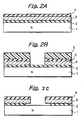
- an oxidation process is performed upon an N-type monocrystalline substrate 1 to form an about 200 to 1000 ⁇ thick silicon oxide layer 2.
- an about 1000 to 3000 ⁇ thick boron-doped polycrystalline silicon layer 3 is deposited on the silicon oxide layer 2.
- an 500 to 3000 ⁇ thick silicon nitride layer 4 is deposited on the boron-doped polycrystalline silicon layer 3.
- an about 1 ⁇ m thick photoresist pattern layer 5 is formed on the silicon nitride layer 4 by using a photolithography process. Then, the silicon nitride layer 4 and the boron-doped polycrystalline silicon layer 3 are etched by a dry etching process using the photoresist pattern layer 5 as a mask. Thus, an opening is perforated within the silicon nitride layer 4 and the boron-doped polycrystalline silicon layer 2. Then, the photoresist pattern layer 5 is removed.
- Fig. 2C in the same way as in Fig. 1C, as about 1000 to 3000 ⁇ thickness of the silicon oxide layer 2 is side-etched by a wet etching process using the silicon nitride layer 4 and the boron-doped polycrystalline silicon layer 3 as a mask.
- the silicon oxide layer 6a is etched by a wet etching process using hydrogen fluoride.
- the non-doped polycrystalline silicon layer 6 is left only on the sidewalls of the silicon oxide layer 2. Note that in this case, the monocrystallines silicon substrate 1 is hardly etched.
- boron ions are implanted into the monocrystalline silicon substrate 1 by using the silicon nitride layer 4 as a mask. As a result, a P-type base layer 7 is formed within the monocrystalline silicon substrate 1.
- an about 200 to 1000 ⁇ thick silicon oxide layer 8 and an about 500 to 3000 ⁇ thick silicon nitride layer 9 are sequentially deposited on the entire surface.
- the silicon nitride layer 9 is etched back by a dry etching process, and thereafter, the silicon oxide layer 8 is etched by a wet etching process. As a result, a sidewall insulating layer is formed by the silicon oxide layer 8 and the silicon nitride layer 9.
- Fig. 2J in the same way as in Fig. 1I, an about 1000 to 3000 ⁇ thick polycrystalline silicon layer 10 is deposited on the entire surface, and then, arsenic ions are implanted into the polycrystalline silicon layer 10. Then, the polycrystalline silicon layer 10 is patterned by a photolithography and etching process. As a result, the arsenic-doped polycrystalline silicon layer 10 is formed.
- annealing operation to a temperature of about 700 to 1200°C is carried out.
- boron ions are diffused from the boron-doped polycrystalline silicon layer 3 via the non-doped polycrystalline silicon layer 6 to the monocrystalline silicon substrate 1, to thereby form a P + -type graft base region 11 within the monocrystalline silicon substrate 1.
- arsenic ions are diffused from the arsenic-doped polycrystalline silicon layer 10 to the P-type base layer 7, to thereby form an N-type emitter region 12 within the P-type base layer 7.
- an emitter electrode 13E and a base electrode 13B are formed.
- the base electrode 13B is connected via the polycrystalline silicon layers 3 and 6 to the graft base region 11.
- an NPN-type transistor having the monocrystalline silicon substrate 1 as a collector connected to a collector electrode (not shown) is completed.
- the introduction of impurity ions into the polycrystalline silicon layers 3 and 10 can be carried out simultaneously with the growth thereof or by the ion implantation after the growth thereof.
- the manufacturing cost can be dereased.
- the present invention can also be applied to a collector-buried-layer type bipolar transistor where a pull-out collector electrode is formed on the front surface of a monocrystalline silicon substrate.
- the present invention can be applied to a method for manufacturing a PNP-type transistor.
Landscapes
- Bipolar Transistors (AREA)
Applications Claiming Priority (2)
| Application Number | Priority Date | Filing Date | Title |
|---|---|---|---|
| JP8471398 | 1998-03-30 | ||
| JP10084713A JP3005517B2 (ja) | 1998-03-30 | 1998-03-30 | 半導体装置の製造方法 |
Publications (2)
| Publication Number | Publication Date |
|---|---|
| EP0948040A1 true EP0948040A1 (de) | 1999-10-06 |
| EP0948040B1 EP0948040B1 (de) | 2002-06-12 |
Family
ID=13838320
Family Applications (1)
| Application Number | Title | Priority Date | Filing Date |
|---|---|---|---|
| EP99106474A Expired - Lifetime EP0948040B1 (de) | 1998-03-30 | 1999-03-30 | Methode zur Herstellung eines Bipolartransistors mit Eigenschaften zur Unterdrückung der Verschlechterung von Transistor-Charakteristiken |
Country Status (7)
| Country | Link |
|---|---|
| US (1) | US6124181A (de) |
| EP (1) | EP0948040B1 (de) |
| JP (1) | JP3005517B2 (de) |
| KR (1) | KR100301531B1 (de) |
| CN (1) | CN1129174C (de) |
| DE (1) | DE69901752T2 (de) |
| TW (1) | TW417275B (de) |
Families Citing this family (6)
| Publication number | Priority date | Publication date | Assignee | Title |
|---|---|---|---|---|
| EP1082758A2 (de) * | 1998-11-13 | 2001-03-14 | Koninklijke Philips Electronics N.V. | Verfahren zur herstellung einer halbleiteranordnung mit einem bipolartransistor |
| EP1630863B1 (de) * | 2004-08-31 | 2014-05-14 | Infineon Technologies AG | Verfahren zur Herstellung eines monolithisch integrierten vertikalen Halbleiterbauteils in einem SOI-Substrat |
| US7300850B2 (en) * | 2005-09-30 | 2007-11-27 | Semiconductor Components Industries, L.L.C. | Method of forming a self-aligned transistor |
| DE102007010563A1 (de) * | 2007-02-22 | 2008-08-28 | IHP GmbH - Innovations for High Performance Microelectronics/Institut für innovative Mikroelektronik | Selektives Wachstum von polykristallinem siliziumhaltigen Halbleitermaterial auf siliziumhaltiger Halbleiteroberfläche |
| JP5239254B2 (ja) * | 2007-08-22 | 2013-07-17 | サンケン電気株式会社 | 絶縁ゲート型半導体素子の製造方法 |
| CN105097506B (zh) * | 2014-04-29 | 2018-11-27 | 无锡华润上华科技有限公司 | 多晶硅发射极垂直npn晶体管的制造方法 |
Citations (3)
| Publication number | Priority date | Publication date | Assignee | Title |
|---|---|---|---|---|
| JPS62169364A (ja) * | 1985-07-31 | 1987-07-25 | Hitachi Denshi Ltd | 半導体装置の製造方法 |
| US5523245A (en) * | 1994-05-12 | 1996-06-04 | Nec Corporation | Process for fabricating high-performance facet-free small-sized bipolar transistor |
| EP0768716A2 (de) * | 1995-10-16 | 1997-04-16 | Nec Corporation | Bipolartransistor und Verfahren zur Herstellung |
Family Cites Families (7)
| Publication number | Priority date | Publication date | Assignee | Title |
|---|---|---|---|---|
| JPH04122029A (ja) * | 1990-09-13 | 1992-04-22 | Nec Corp | 半導体装置の製造方法 |
| JPH04192335A (ja) * | 1990-11-24 | 1992-07-10 | Nec Corp | 半導体装置の製造方法 |
| JPH0669217A (ja) * | 1992-08-20 | 1994-03-11 | Fujitsu Ltd | 半導体装置の製造方法 |
| JPH06168951A (ja) * | 1992-12-01 | 1994-06-14 | Fujitsu Ltd | 半導体装置の製造方法 |
| JPH06275633A (ja) * | 1993-03-22 | 1994-09-30 | Miyazaki Oki Electric Co Ltd | バイポーラ型半導体装置およびその製造方法 |
| JPH0766214A (ja) * | 1993-08-26 | 1995-03-10 | Oki Electric Ind Co Ltd | バイポーラ型半導体集積回路装置の製造方法 |
| US5523244A (en) * | 1994-12-19 | 1996-06-04 | Hughes Aircraft Company | Transistor fabrication method using dielectric protection layers to eliminate emitter defects |
-
1998
- 1998-03-30 JP JP10084713A patent/JP3005517B2/ja not_active Expired - Fee Related
-
1999
- 1999-03-29 TW TW088105054A patent/TW417275B/zh not_active IP Right Cessation
- 1999-03-29 KR KR1019990010768A patent/KR100301531B1/ko not_active Expired - Fee Related
- 1999-03-30 EP EP99106474A patent/EP0948040B1/de not_active Expired - Lifetime
- 1999-03-30 DE DE69901752T patent/DE69901752T2/de not_active Expired - Fee Related
- 1999-03-30 US US09/281,286 patent/US6124181A/en not_active Expired - Fee Related
- 1999-03-30 CN CN99103424A patent/CN1129174C/zh not_active Expired - Fee Related
Patent Citations (3)
| Publication number | Priority date | Publication date | Assignee | Title |
|---|---|---|---|---|
| JPS62169364A (ja) * | 1985-07-31 | 1987-07-25 | Hitachi Denshi Ltd | 半導体装置の製造方法 |
| US5523245A (en) * | 1994-05-12 | 1996-06-04 | Nec Corporation | Process for fabricating high-performance facet-free small-sized bipolar transistor |
| EP0768716A2 (de) * | 1995-10-16 | 1997-04-16 | Nec Corporation | Bipolartransistor und Verfahren zur Herstellung |
Non-Patent Citations (1)
| Title |
|---|
| PATENT ABSTRACTS OF JAPAN vol. 012, no. 009 (E - 572) 12 January 1988 (1988-01-12) * |
Also Published As
| Publication number | Publication date |
|---|---|
| JP3005517B2 (ja) | 2000-01-31 |
| JPH11283991A (ja) | 1999-10-15 |
| US6124181A (en) | 2000-09-26 |
| DE69901752T2 (de) | 2003-02-06 |
| KR100301531B1 (ko) | 2001-10-29 |
| DE69901752D1 (de) | 2002-07-18 |
| TW417275B (en) | 2001-01-01 |
| EP0948040B1 (de) | 2002-06-12 |
| KR19990078358A (ko) | 1999-10-25 |
| CN1129174C (zh) | 2003-11-26 |
| CN1230771A (zh) | 1999-10-06 |
Similar Documents
| Publication | Publication Date | Title |
|---|---|---|
| US5391503A (en) | Method of forming a stacked semiconductor device wherein semiconductor layers and insulating films are sequentially stacked and forming openings through such films and etchings using one of the insulating films as a mask | |
| JP3098848B2 (ja) | 自己整合型プレーナモノリシック集積回路縦型トランジスタプロセス | |
| EP0948040B1 (de) | Methode zur Herstellung eines Bipolartransistors mit Eigenschaften zur Unterdrückung der Verschlechterung von Transistor-Charakteristiken | |
| US5324672A (en) | Manufacturing method for bipolar transistor | |
| US20010022386A1 (en) | Bipolar transistor having recessed and rounded surface and its manufacturing method | |
| US5747374A (en) | Methods of fabricating bipolar transistors having separately formed intrinsic base and link-up regions | |
| US6444536B2 (en) | Method for fabricating bipolar transistors | |
| US6060365A (en) | Method for fabricating a bipolar transistor | |
| JPH10189765A (ja) | 半導体装置の製造方法 | |
| JP3349198B2 (ja) | バイポ−ラトランジスタの製造方法 | |
| EP1039532A2 (de) | Herstellungsverfahren für Halbleiterbauelemente vom bipolaren Typ | |
| JP3186676B2 (ja) | 半導体装置の構造と製法 | |
| JP3537494B2 (ja) | 半導体装置および半導体装置の製造方法 | |
| US6579774B2 (en) | Semiconductor device fabrication method | |
| JPH02153534A (ja) | 半導体装置の製造方法 | |
| JPH1174366A (ja) | 半導体装置およびその製造方法 | |
| JP2519251B2 (ja) | 半導体集積回路装置の製造方法 | |
| JP2644201B2 (ja) | 半導体装置の製造方法 | |
| JPH05235009A (ja) | 半導体集積回路装置の製造方法 | |
| JPS6295871A (ja) | 半導体装置の製造方法 | |
| JPH09232330A (ja) | 半導体装置の製造方法 | |
| JP2001068478A (ja) | 半導体装置およびその製造方法 | |
| JPH1092831A (ja) | バイポーラトランジスタの製造方法 | |
| JPH0628262B2 (ja) | 半導体装置の製造方法 | |
| JPH0654776B2 (ja) | 半導体装置の製造方法 |
Legal Events
| Date | Code | Title | Description |
|---|---|---|---|
| PUAI | Public reference made under article 153(3) epc to a published international application that has entered the european phase |
Free format text: ORIGINAL CODE: 0009012 |
|
| AK | Designated contracting states |
Kind code of ref document: A1 Designated state(s): DE FR GB |
|
| AX | Request for extension of the european patent |
Free format text: AL;LT;LV;MK;RO;SI |
|
| 17P | Request for examination filed |
Effective date: 19991213 |
|
| AKX | Designation fees paid |
Free format text: DE FR GB |
|
| GRAG | Despatch of communication of intention to grant |
Free format text: ORIGINAL CODE: EPIDOS AGRA |
|
| 17Q | First examination report despatched |
Effective date: 20010713 |
|
| GRAG | Despatch of communication of intention to grant |
Free format text: ORIGINAL CODE: EPIDOS AGRA |
|
| GRAH | Despatch of communication of intention to grant a patent |
Free format text: ORIGINAL CODE: EPIDOS IGRA |
|
| GRAH | Despatch of communication of intention to grant a patent |
Free format text: ORIGINAL CODE: EPIDOS IGRA |
|
| GRAA | (expected) grant |
Free format text: ORIGINAL CODE: 0009210 |
|
| AK | Designated contracting states |
Kind code of ref document: B1 Designated state(s): DE FR GB |
|
| REG | Reference to a national code |
Ref country code: GB Ref legal event code: FG4D |
|
| REF | Corresponds to: |
Ref document number: 69901752 Country of ref document: DE Date of ref document: 20020718 |
|
| ET | Fr: translation filed | ||
| PGFP | Annual fee paid to national office [announced via postgrant information from national office to epo] |
Ref country code: FR Payment date: 20030310 Year of fee payment: 5 |
|
| PGFP | Annual fee paid to national office [announced via postgrant information from national office to epo] |
Ref country code: GB Payment date: 20030326 Year of fee payment: 5 |
|
| REG | Reference to a national code |
Ref country code: GB Ref legal event code: 732E |
|
| PGFP | Annual fee paid to national office [announced via postgrant information from national office to epo] |
Ref country code: DE Payment date: 20030410 Year of fee payment: 5 |
|
| PLBE | No opposition filed within time limit |
Free format text: ORIGINAL CODE: 0009261 |
|
| STAA | Information on the status of an ep patent application or granted ep patent |
Free format text: STATUS: NO OPPOSITION FILED WITHIN TIME LIMIT |
|
| 26N | No opposition filed |
Effective date: 20030313 |
|
| REG | Reference to a national code |
Ref country code: FR Ref legal event code: TP |
|
| PG25 | Lapsed in a contracting state [announced via postgrant information from national office to epo] |
Ref country code: GB Free format text: LAPSE BECAUSE OF NON-PAYMENT OF DUE FEES Effective date: 20040330 |
|
| PG25 | Lapsed in a contracting state [announced via postgrant information from national office to epo] |
Ref country code: DE Free format text: LAPSE BECAUSE OF NON-PAYMENT OF DUE FEES Effective date: 20041001 |
|
| GBPC | Gb: european patent ceased through non-payment of renewal fee |
Effective date: 20040330 |
|
| PG25 | Lapsed in a contracting state [announced via postgrant information from national office to epo] |
Ref country code: FR Free format text: LAPSE BECAUSE OF NON-PAYMENT OF DUE FEES Effective date: 20041130 |
|
| REG | Reference to a national code |
Ref country code: FR Ref legal event code: ST |