EP0948048A1 - Boítier à dimensions de puce - Google Patents
Boítier à dimensions de puce Download PDFInfo
- Publication number
- EP0948048A1 EP0948048A1 EP98302098A EP98302098A EP0948048A1 EP 0948048 A1 EP0948048 A1 EP 0948048A1 EP 98302098 A EP98302098 A EP 98302098A EP 98302098 A EP98302098 A EP 98302098A EP 0948048 A1 EP0948048 A1 EP 0948048A1
- Authority
- EP
- European Patent Office
- Prior art keywords
- chip
- package
- package frame
- frame
- chip scale
- Prior art date
- Legal status (The legal status is an assumption and is not a legal conclusion. Google has not performed a legal analysis and makes no representation as to the accuracy of the status listed.)
- Withdrawn
Links
Images


Classifications
-
- H—ELECTRICITY
- H10—SEMICONDUCTOR DEVICES; ELECTRIC SOLID-STATE DEVICES NOT OTHERWISE PROVIDED FOR
- H10W—GENERIC PACKAGES, INTERCONNECTIONS, CONNECTORS OR OTHER CONSTRUCTIONAL DETAILS OF DEVICES COVERED BY CLASS H10
- H10W70/00—Package substrates; Interposers; Redistribution layers [RDL]
- H10W70/40—Leadframes
- H10W70/411—Chip-supporting parts, e.g. die pads
- H10W70/415—Leadframe inner leads serving as die pads
-
- H—ELECTRICITY
- H10—SEMICONDUCTOR DEVICES; ELECTRIC SOLID-STATE DEVICES NOT OTHERWISE PROVIDED FOR
- H10W—GENERIC PACKAGES, INTERCONNECTIONS, CONNECTORS OR OTHER CONSTRUCTIONAL DETAILS OF DEVICES COVERED BY CLASS H10
- H10W72/00—Interconnections or connectors in packages
- H10W72/50—Bond wires
- H10W72/531—Shapes of wire connectors
- H10W72/536—Shapes of wire connectors the connected ends being ball-shaped
-
- H—ELECTRICITY
- H10—SEMICONDUCTOR DEVICES; ELECTRIC SOLID-STATE DEVICES NOT OTHERWISE PROVIDED FOR
- H10W—GENERIC PACKAGES, INTERCONNECTIONS, CONNECTORS OR OTHER CONSTRUCTIONAL DETAILS OF DEVICES COVERED BY CLASS H10
- H10W72/00—Interconnections or connectors in packages
- H10W72/50—Bond wires
- H10W72/531—Shapes of wire connectors
- H10W72/5363—Shapes of wire connectors the connected ends being wedge-shaped
-
- H—ELECTRICITY
- H10—SEMICONDUCTOR DEVICES; ELECTRIC SOLID-STATE DEVICES NOT OTHERWISE PROVIDED FOR
- H10W—GENERIC PACKAGES, INTERCONNECTIONS, CONNECTORS OR OTHER CONSTRUCTIONAL DETAILS OF DEVICES COVERED BY CLASS H10
- H10W72/00—Interconnections or connectors in packages
- H10W72/50—Bond wires
- H10W72/541—Dispositions of bond wires
- H10W72/5445—Dispositions of bond wires being orthogonal to a side surface of the chip, e.g. parallel arrangements
-
- H—ELECTRICITY
- H10—SEMICONDUCTOR DEVICES; ELECTRIC SOLID-STATE DEVICES NOT OTHERWISE PROVIDED FOR
- H10W—GENERIC PACKAGES, INTERCONNECTIONS, CONNECTORS OR OTHER CONSTRUCTIONAL DETAILS OF DEVICES COVERED BY CLASS H10
- H10W72/00—Interconnections or connectors in packages
- H10W72/50—Bond wires
- H10W72/551—Materials of bond wires
- H10W72/552—Materials of bond wires comprising metals or metalloids, e.g. silver
- H10W72/5522—Materials of bond wires comprising metals or metalloids, e.g. silver comprising gold [Au]
-
- H—ELECTRICITY
- H10—SEMICONDUCTOR DEVICES; ELECTRIC SOLID-STATE DEVICES NOT OTHERWISE PROVIDED FOR
- H10W—GENERIC PACKAGES, INTERCONNECTIONS, CONNECTORS OR OTHER CONSTRUCTIONAL DETAILS OF DEVICES COVERED BY CLASS H10
- H10W72/00—Interconnections or connectors in packages
- H10W72/851—Dispositions of multiple connectors or interconnections
- H10W72/853—On the same surface
- H10W72/865—Die-attach connectors and bond wires
-
- H—ELECTRICITY
- H10—SEMICONDUCTOR DEVICES; ELECTRIC SOLID-STATE DEVICES NOT OTHERWISE PROVIDED FOR
- H10W—GENERIC PACKAGES, INTERCONNECTIONS, CONNECTORS OR OTHER CONSTRUCTIONAL DETAILS OF DEVICES COVERED BY CLASS H10
- H10W72/00—Interconnections or connectors in packages
- H10W72/90—Bond pads, in general
- H10W72/931—Shapes of bond pads
- H10W72/932—Plan-view shape, i.e. in top view
-
- H—ELECTRICITY
- H10—SEMICONDUCTOR DEVICES; ELECTRIC SOLID-STATE DEVICES NOT OTHERWISE PROVIDED FOR
- H10W—GENERIC PACKAGES, INTERCONNECTIONS, CONNECTORS OR OTHER CONSTRUCTIONAL DETAILS OF DEVICES COVERED BY CLASS H10
- H10W90/00—Package configurations
- H10W90/701—Package configurations characterised by the relative positions of pads or connectors relative to package parts
- H10W90/731—Package configurations characterised by the relative positions of pads or connectors relative to package parts of die-attach connectors
- H10W90/736—Package configurations characterised by the relative positions of pads or connectors relative to package parts of die-attach connectors between a chip and a stacked lead frame, conducting package substrate or heat sink
-
- H—ELECTRICITY
- H10—SEMICONDUCTOR DEVICES; ELECTRIC SOLID-STATE DEVICES NOT OTHERWISE PROVIDED FOR
- H10W—GENERIC PACKAGES, INTERCONNECTIONS, CONNECTORS OR OTHER CONSTRUCTIONAL DETAILS OF DEVICES COVERED BY CLASS H10
- H10W90/00—Package configurations
- H10W90/701—Package configurations characterised by the relative positions of pads or connectors relative to package parts
- H10W90/751—Package configurations characterised by the relative positions of pads or connectors relative to package parts of bond wires
- H10W90/756—Package configurations characterised by the relative positions of pads or connectors relative to package parts of bond wires between a chip and a stacked lead frame, conducting package substrate or heat sink
Definitions
- the invention generally relates to an integrated circuit(IC) package, and particularly to a chip scale package of semiconductor device.
- each bonding point of the IC chip to be packaged is connected with an inner lead through a bonding wire (such as a gold wire).
- a bonding wire such as a gold wire.
- each outer lead which is an extension of an inner lead can be welded into a connection point of a circuit board, a signal path can thus be built to conduct signal between a bonding point of the packaged IC chip and a corresponding connecting point of the circuit board.
- encapsulant such as epoxy is used to cover the top of the IC chip.
- the object of the present invention is to provide a new IC package structure with thin and super-mini size, and with features for overcoming the disadvantages inherent in a conventional IC package structure.
- Another object of the present invention is to provide a new IC package structure allowing an IC package to be used for IC chip of various sizes, and therefore allowing lower production/storage cost.
- a chip scale package structure based on the present invention for packaging an IC chip is characterized by that:
- Another version of the chip scale package structure based on the present invention for packaging an IC chip is characterized by that:
- the chip scale package according to the present invention may also be configured to further comprise material covering the top surface of the IC chip, thereby the bonding wire and the bonding points can be protected.
- the chip scale package based on the present invention may be so configured that the magnitudes of the gap and the angle are in such a range that a stress caused by a difference in coefficient of thermal expansion/shrinkage between the IC chip and the package frame can be perfectly cushioned.
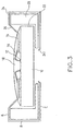
- FIG. 1 A preferred embodiment of the chip scale package based on the invention is illustrated by Fig. 1, Fig. 2, and Fig. 3.
- the bonding points 12 on the top of IC chip 10 are connected with inner lead 14 through bonding wires 16 (such as gold wires).
- Material such as epoxy is used to cover the top of IC chip 10 for preventing bonding 16 wires from being damaged in production processing or product application phase.
- IC chip 10 is surrounded by a package frame 20 with a gap 22 between them (between IC chip 10 and package frame 20).
- Package frame 20 is made of material with high electrical conductivity and heat dissipation capability, and has its surface processed for insulation capability, resulting in good heat dissipating for an operating IC chip, and lower induction for outer lead 24, and consequently higher operating reliability and better quality of signal communication can be achieved.
- Inner lead 14 and outer lead 24, connected by a connecting segment 26, can be deemed an element in spite of different names assigned for the reason they are differently located.
- Connecting segment 26 is configured to slant, with upper end connected with outer lead 24 and lower end connected with inner lead 14.
- Outer lead 24 extends along the outer surface of package frame 20 (of course bends according to the shape of package frame 20), and ends under IC chip 10 to hook upward for fixing package frame 20 (to hook the end of the part of package frame 20 which is under IC chip 10, for example), or for limiting package frame 20 to an optimum working position (or region).
- a (top segment of outer lead 24), B (side segment of outer lead 24), and C (bottom segment of outer lead 24) are available for welding, thereby an IC package so configured can adapt to various applications in which different portions of an IC package is to be selected for welding operation.
- outer lead 24 can resist high pressure in molding, testing, and welding processes. Pressure may be exerted on A (top segment of outer lead 24), B (side segment of outer lead 24), and C (bottom segment of outer lead 24) of outer lead 24 to make them stick evenly to the surface of package frame 20, thereby to realize a perfect contact between outer lead 24 and the face of an object whenever necessary.
- a (top segment of outer lead 24), or B(side segment of outer lead 24), or C (bottom segment of outer lead 24) of all outer leads 24 can be easily adjusted to be on the same plane (all outer leads 24 with A on the same plane, with B on another plane, foe example), to achieve optimum contacting between outer lead 24 and the object to be welded. It is clear the chip scale package structure based on the present invention can solve a troublesome problem that a conventional IC package hardly has its all package leads lying on the sane plane.
- a (top segment of outer lead 24), B (side segment of outer lead 24), and C (bottom segment of outer lead 24) of outer lead 24 can be prevented form reaching IC chip 10 according to the structure ( gap 22 contributes to this effect, for example). It can be seen now the chip scale package structure based on the invention provides an IC package with high reliability, pressure resistance, and significant convenience of welding operation for various applications.
- thermal coefficient of package frame 20 is bigger than IC chip 10
- IC chip 10 generates heat when operating
- package frame 20 will expand outward more than IC chip 10 then (magnitude of expansion size of package frame 20 is bigger than that of IC chip 10), resulting in smaller slant angle of connecting segment 26 connecting inner lead 14 and outer lead 24, consequently leading to moving of IC chip 10 upward, and buffer (or cushioning) for stress
- IC chip 10 cools as a result of being idle (not operating)
- package frame 20 shrinks inward more than IC chip 10 then ( magnitude of shrinkage of package frame 20 is bigger than that of IC chip 10), leading to bigger slant angle of connecting segment 26, consequently IC chip 10 moves downward and buffer (or cushioning) for stress is provided.
Landscapes
- Lead Frames For Integrated Circuits (AREA)
Priority Applications (1)
| Application Number | Priority Date | Filing Date | Title |
|---|---|---|---|
| EP98302098A EP0948048A1 (fr) | 1998-03-20 | 1998-03-20 | Boítier à dimensions de puce |
Applications Claiming Priority (1)
| Application Number | Priority Date | Filing Date | Title |
|---|---|---|---|
| EP98302098A EP0948048A1 (fr) | 1998-03-20 | 1998-03-20 | Boítier à dimensions de puce |
Publications (1)
| Publication Number | Publication Date |
|---|---|
| EP0948048A1 true EP0948048A1 (fr) | 1999-10-06 |
Family
ID=8234722
Family Applications (1)
| Application Number | Title | Priority Date | Filing Date |
|---|---|---|---|
| EP98302098A Withdrawn EP0948048A1 (fr) | 1998-03-20 | 1998-03-20 | Boítier à dimensions de puce |
Country Status (1)
| Country | Link |
|---|---|
| EP (1) | EP0948048A1 (fr) |
Cited By (6)
| Publication number | Priority date | Publication date | Assignee | Title |
|---|---|---|---|---|
| US6320251B1 (en) | 2000-01-18 | 2001-11-20 | Amkor Technology, Inc. | Stackable package for an integrated circuit |
| US6404046B1 (en) | 2000-02-03 | 2002-06-11 | Amkor Technology, Inc. | Module of stacked integrated circuit packages including an interposer |
| US6518659B1 (en) | 2000-05-08 | 2003-02-11 | Amkor Technology, Inc. | Stackable package having a cavity and a lid for an electronic device |
| US6667544B1 (en) | 2000-06-30 | 2003-12-23 | Amkor Technology, Inc. | Stackable package having clips for fastening package and tool for opening clips |
| US6977431B1 (en) | 2003-11-05 | 2005-12-20 | Amkor Technology, Inc. | Stackable semiconductor package and manufacturing method thereof |
| US7009296B1 (en) | 2004-01-15 | 2006-03-07 | Amkor Technology, Inc. | Semiconductor package with substrate coupled to a peripheral side surface of a semiconductor die |
Citations (7)
| Publication number | Priority date | Publication date | Assignee | Title |
|---|---|---|---|---|
| US5347159A (en) * | 1990-09-24 | 1994-09-13 | Tessera, Inc. | Semiconductor chip assemblies with face-up mounting and rear-surface connection to substrate |
| US5362656A (en) * | 1992-12-02 | 1994-11-08 | Intel Corporation | Method of making an electronic assembly having a flexible circuit wrapped around a substrate |
| JPH0778925A (ja) * | 1993-09-06 | 1995-03-20 | Matsushita Electric Ind Co Ltd | 半導体装置およびその製造方法 |
| JPH07249725A (ja) * | 1994-03-11 | 1995-09-26 | Furukawa Electric Co Ltd:The | 表面実装型電子部品 |
| JPH0817864A (ja) * | 1994-06-24 | 1996-01-19 | New Japan Radio Co Ltd | 半導体パッケ−ジ |
| JPH08213424A (ja) * | 1995-02-02 | 1996-08-20 | Fujitsu Ltd | 半導体装置 |
| JPH0992769A (ja) * | 1995-09-22 | 1997-04-04 | Hitachi Cable Ltd | 半導体装置 |
-
1998
- 1998-03-20 EP EP98302098A patent/EP0948048A1/fr not_active Withdrawn
Patent Citations (7)
| Publication number | Priority date | Publication date | Assignee | Title |
|---|---|---|---|---|
| US5347159A (en) * | 1990-09-24 | 1994-09-13 | Tessera, Inc. | Semiconductor chip assemblies with face-up mounting and rear-surface connection to substrate |
| US5362656A (en) * | 1992-12-02 | 1994-11-08 | Intel Corporation | Method of making an electronic assembly having a flexible circuit wrapped around a substrate |
| JPH0778925A (ja) * | 1993-09-06 | 1995-03-20 | Matsushita Electric Ind Co Ltd | 半導体装置およびその製造方法 |
| JPH07249725A (ja) * | 1994-03-11 | 1995-09-26 | Furukawa Electric Co Ltd:The | 表面実装型電子部品 |
| JPH0817864A (ja) * | 1994-06-24 | 1996-01-19 | New Japan Radio Co Ltd | 半導体パッケ−ジ |
| JPH08213424A (ja) * | 1995-02-02 | 1996-08-20 | Fujitsu Ltd | 半導体装置 |
| JPH0992769A (ja) * | 1995-09-22 | 1997-04-04 | Hitachi Cable Ltd | 半導体装置 |
Non-Patent Citations (5)
| Title |
|---|
| PATENT ABSTRACTS OF JAPAN vol. 095, no. 006 31 July 1995 (1995-07-31) * |
| PATENT ABSTRACTS OF JAPAN vol. 096, no. 001 31 January 1996 (1996-01-31) * |
| PATENT ABSTRACTS OF JAPAN vol. 096, no. 005 31 May 1996 (1996-05-31) * |
| PATENT ABSTRACTS OF JAPAN vol. 096, no. 012 26 December 1996 (1996-12-26) * |
| PATENT ABSTRACTS OF JAPAN vol. 097, no. 008 29 August 1997 (1997-08-29) * |
Cited By (6)
| Publication number | Priority date | Publication date | Assignee | Title |
|---|---|---|---|---|
| US6320251B1 (en) | 2000-01-18 | 2001-11-20 | Amkor Technology, Inc. | Stackable package for an integrated circuit |
| US6404046B1 (en) | 2000-02-03 | 2002-06-11 | Amkor Technology, Inc. | Module of stacked integrated circuit packages including an interposer |
| US6518659B1 (en) | 2000-05-08 | 2003-02-11 | Amkor Technology, Inc. | Stackable package having a cavity and a lid for an electronic device |
| US6667544B1 (en) | 2000-06-30 | 2003-12-23 | Amkor Technology, Inc. | Stackable package having clips for fastening package and tool for opening clips |
| US6977431B1 (en) | 2003-11-05 | 2005-12-20 | Amkor Technology, Inc. | Stackable semiconductor package and manufacturing method thereof |
| US7009296B1 (en) | 2004-01-15 | 2006-03-07 | Amkor Technology, Inc. | Semiconductor package with substrate coupled to a peripheral side surface of a semiconductor die |
Similar Documents
| Publication | Publication Date | Title |
|---|---|---|
| US5479050A (en) | Leadframe with pedestal | |
| US6919628B2 (en) | Stack chip package structure | |
| JPS63148670A (ja) | リ−ドフレ−ム材 | |
| US8445998B1 (en) | Leadframe structures for semiconductor packages | |
| JP5121354B2 (ja) | オーバーモールドmcmicパッケージおよびその作製方法 | |
| US6087586A (en) | Chip scale package | |
| EP0948048A1 (fr) | Boítier à dimensions de puce | |
| US5874783A (en) | Semiconductor device having the inner end of connector leads displaced onto the surface of semiconductor chip | |
| KR960004559B1 (ko) | 수지 봉지형 반도체 장치 및 그 제조 방법 | |
| US20070096297A1 (en) | RF power transistor package | |
| WO2008083146A1 (fr) | Grille de connexion résistant aux contraintes et procédé | |
| US20230326838A1 (en) | Discrete power semiconductor package | |
| US9269594B2 (en) | High power ceramic on copper package | |
| US20050285240A1 (en) | Semiconductor device and method of manufacturing the same | |
| KR19990041371U (ko) | 칩 스케일 패키지 | |
| KR102359873B1 (ko) | 패키지 기판 및 이를 포함하는 반도체 패키지 | |
| US6621151B1 (en) | Lead frame for an integrated circuit chip | |
| KR0156335B1 (ko) | 타이 바를 이용한 반도체 칩 패키지 | |
| KR200347457Y1 (ko) | 내장형 패키지에 의한 반도체 장치 | |
| US6583501B2 (en) | Lead frame for an integrated circuit chip (integrated circuit peripheral support) | |
| JP6887476B2 (ja) | 半導体パワーモジュール | |
| KR100475340B1 (ko) | 리드온칩패키지 | |
| KR100216843B1 (ko) | 리드프레임의 구조 및 이를 이용한 반도체 패키지 | |
| JPH0831986A (ja) | 放熱板付半導体装置 | |
| JP2795245B2 (ja) | 樹脂封止型半導体装置 |
Legal Events
| Date | Code | Title | Description |
|---|---|---|---|
| PUAI | Public reference made under article 153(3) epc to a published international application that has entered the european phase |
Free format text: ORIGINAL CODE: 0009012 |
|
| AK | Designated contracting states |
Kind code of ref document: A1 Designated state(s): AT BE CH DE DK ES FI FR GB GR IE IT LI LU MC NL PT SE |
|
| AX | Request for extension of the european patent |
Free format text: AL;LT;LV;MK;RO;SI |
|
| AKX | Designation fees paid | ||
| REG | Reference to a national code |
Ref country code: DE Ref legal event code: 8566 |
|
| STAA | Information on the status of an ep patent application or granted ep patent |
Free format text: STATUS: THE APPLICATION IS DEEMED TO BE WITHDRAWN |
|
| 18D | Application deemed to be withdrawn |
Effective date: 20001003 |