EP0948051A2 - Dispositif semi-conducteur ayant un circuit de protection - Google Patents
Dispositif semi-conducteur ayant un circuit de protection Download PDFInfo
- Publication number
- EP0948051A2 EP0948051A2 EP99105958A EP99105958A EP0948051A2 EP 0948051 A2 EP0948051 A2 EP 0948051A2 EP 99105958 A EP99105958 A EP 99105958A EP 99105958 A EP99105958 A EP 99105958A EP 0948051 A2 EP0948051 A2 EP 0948051A2
- Authority
- EP
- European Patent Office
- Prior art keywords
- region
- semiconductor device
- guard ring
- protective
- well
- Prior art date
- Legal status (The legal status is an assumption and is not a legal conclusion. Google has not performed a legal analysis and makes no representation as to the accuracy of the status listed.)
- Granted
Links
Images




Classifications
-
- H—ELECTRICITY
- H10—SEMICONDUCTOR DEVICES; ELECTRIC SOLID-STATE DEVICES NOT OTHERWISE PROVIDED FOR
- H10D—INORGANIC ELECTRIC SEMICONDUCTOR DEVICES
- H10D89/00—Aspects of integrated devices not covered by groups H10D84/00 - H10D88/00
- H10D89/60—Integrated devices comprising arrangements for electrical or thermal protection, e.g. protection circuits against electrostatic discharge [ESD]
- H10D89/601—Integrated devices comprising arrangements for electrical or thermal protection, e.g. protection circuits against electrostatic discharge [ESD] for devices having insulated gate electrodes, e.g. for IGFETs or IGBTs
- H10D89/911—Integrated devices comprising arrangements for electrical or thermal protection, e.g. protection circuits against electrostatic discharge [ESD] for devices having insulated gate electrodes, e.g. for IGFETs or IGBTs using passive elements as protective elements
-
- H—ELECTRICITY
- H10—SEMICONDUCTOR DEVICES; ELECTRIC SOLID-STATE DEVICES NOT OTHERWISE PROVIDED FOR
- H10P—GENERIC PROCESSES OR APPARATUS FOR THE MANUFACTURE OR TREATMENT OF DEVICES COVERED BY CLASS H10
- H10P10/00—Bonding of wafers, substrates or parts of devices
-
- H—ELECTRICITY
- H10—SEMICONDUCTOR DEVICES; ELECTRIC SOLID-STATE DEVICES NOT OTHERWISE PROVIDED FOR
- H10D—INORGANIC ELECTRIC SEMICONDUCTOR DEVICES
- H10D89/00—Aspects of integrated devices not covered by groups H10D84/00 - H10D88/00
- H10D89/60—Integrated devices comprising arrangements for electrical or thermal protection, e.g. protection circuits against electrostatic discharge [ESD]
- H10D89/601—Integrated devices comprising arrangements for electrical or thermal protection, e.g. protection circuits against electrostatic discharge [ESD] for devices having insulated gate electrodes, e.g. for IGFETs or IGBTs
- H10D89/811—Integrated devices comprising arrangements for electrical or thermal protection, e.g. protection circuits against electrostatic discharge [ESD] for devices having insulated gate electrodes, e.g. for IGFETs or IGBTs using FETs as protective elements
Definitions
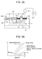
- the present invention provides, in an embodiment thereof, a semiconductor device including a semiconductor substrate having a substrate region of a first conductivity type or a second conductivity type opposite to the first conductivity type, a well region of the first conductivity type formed on a surface region of the semiconductor substrate and having a first impurity concentration, a guard ring of the first conductivity type disposed on a surface region of the semiconductor substrate within the well region, a MOS transistor having source/drain regions of the second conductivity type and surrounded by the well region, and a diffused region disposed between the source/drain regions of the MOS transistor and the guard ring, the diffused region being of the first conductivity type having a second impurity concentration lower than the first concentration or of the second conductivity.
- the semiconductor device according to the present embodiment is similar to the first embodiment except that an N-well 25 implementing a second conductivity type region is provided between the first well region 11a and the second well region 11b. Since the N-well 25 is of a conductivity type opposite that of the first and second well regions 11a and 11b, when a positive ESD surge current enters the first well region 11a, a charge carried by the surge current can move to the N-well 25 but cannot move from the N-well 25 to the second well region 11b. Therefore, the surge current flows to the guard ring 18n via the P-type substrate 10 and the second P-well 11b and then flows to the ground.
Landscapes
- Semiconductor Integrated Circuits (AREA)
- Metal-Oxide And Bipolar Metal-Oxide Semiconductor Integrated Circuits (AREA)
Applications Claiming Priority (2)
| Application Number | Priority Date | Filing Date | Title |
|---|---|---|---|
| JP07517998A JP3237110B2 (ja) | 1998-03-24 | 1998-03-24 | 半導体装置 |
| JP7517998 | 1998-03-24 |
Publications (3)
| Publication Number | Publication Date |
|---|---|
| EP0948051A2 true EP0948051A2 (fr) | 1999-10-06 |
| EP0948051A3 EP0948051A3 (fr) | 2006-04-05 |
| EP0948051B1 EP0948051B1 (fr) | 2015-09-30 |
Family
ID=13568731
Family Applications (1)
| Application Number | Title | Priority Date | Filing Date |
|---|---|---|---|
| EP99105958.5A Expired - Lifetime EP0948051B1 (fr) | 1998-03-24 | 1999-03-24 | Dispositif semi-conducteur ayant un circuit de protection |
Country Status (6)
| Country | Link |
|---|---|
| US (1) | US6469354B1 (fr) |
| EP (1) | EP0948051B1 (fr) |
| JP (1) | JP3237110B2 (fr) |
| KR (1) | KR100341379B1 (fr) |
| CN (1) | CN1144288C (fr) |
| TW (1) | TW404047B (fr) |
Cited By (10)
| Publication number | Priority date | Publication date | Assignee | Title |
|---|---|---|---|---|
| EP1154486A1 (fr) * | 2000-05-08 | 2001-11-14 | Micronas GmbH | Dispositif de protection contre les décharges électrostatiques comprenant des transistors bipolaires paralleles |
| WO2004077499A3 (fr) * | 2003-02-28 | 2004-11-25 | Koninkl Philips Electronics Nv | Procede dit du type tablette de chocolat destine a l'integration de portes logiques simples et doubles dans un ensemble masque |
| WO2006133888A1 (fr) * | 2005-06-14 | 2006-12-21 | Atmel Germany Gmbh | Structure de protection a semi-conducteurs pour decharge electrostatique |
| WO2007043319A1 (fr) * | 2005-09-30 | 2007-04-19 | Ricoh Company, Ltd. | Dispositif à semi-conducteurs |
| EP1359620A3 (fr) * | 2002-04-24 | 2008-07-23 | Texas Instruments Incorporated | Protection contre les ESD des condensateurs pour le découplage de bruit |
| DE10245770B4 (de) * | 2001-09-27 | 2009-01-29 | Samsung Electronics Co., Ltd., Suwon | Ausgangsschaltkreis |
| US20100200921A1 (en) * | 2009-02-06 | 2010-08-12 | Chikashi Fuchigami | Semiconductor device |
| WO2011031349A1 (fr) * | 2009-09-08 | 2011-03-17 | Xilinx, Inc. | Protection partagée contre les décharges électrostatiques pour pilotes de sortie de circuit intégré |
| KR20150109360A (ko) * | 2013-01-18 | 2015-10-01 | 세이코 인스트루 가부시키가이샤 | 반도체 장치 |
| DE102013104268B4 (de) | 2012-10-31 | 2021-11-11 | Taiwan Semiconductor Manufacturing Company, Ltd. | Integrierte Schaltkreisstrukturen, die Basiswiderstandsabstimmungsbereiche aufweisen, und Verfahren zum Ausbilden derselben |
Families Citing this family (41)
| Publication number | Priority date | Publication date | Assignee | Title |
|---|---|---|---|---|
| US6815775B2 (en) * | 2001-02-02 | 2004-11-09 | Industrial Technology Research Institute | ESD protection design with turn-on restraining method and structures |
| JP4852792B2 (ja) * | 2001-03-30 | 2012-01-11 | 株式会社デンソー | 半導体装置の製造方法 |
| US6730967B2 (en) * | 2001-05-24 | 2004-05-04 | Winbond Electronics Corp. | Electrostatic discharge protection devices and methods for the formation thereof |
| US6534834B1 (en) | 2001-12-19 | 2003-03-18 | Agere Systems, Inc. | Polysilicon bounded snapback device |
| US6621133B1 (en) * | 2002-05-09 | 2003-09-16 | United Microelectronics Corp. | Electrostatic discharge protection device |
| US6730969B1 (en) * | 2002-06-27 | 2004-05-04 | National Semiconductor Corporation | Radiation hardened MOS transistor |
| US7132696B2 (en) * | 2002-08-28 | 2006-11-07 | Micron Technology, Inc. | Intermeshed guard bands for multiple voltage supply structures on an integrated circuit, and methods of making same |
| JP4127007B2 (ja) * | 2002-09-30 | 2008-07-30 | ミツミ電機株式会社 | 半導体装置 |
| JP3713013B2 (ja) | 2002-12-06 | 2005-11-02 | 松下電器産業株式会社 | 半導体集積回路装置の製造方法 |
| US7244992B2 (en) | 2003-07-17 | 2007-07-17 | Ming-Dou Ker | Turn-on-efficient bipolar structures with deep N-well for on-chip ESD protection |
| US20050045952A1 (en) * | 2003-08-27 | 2005-03-03 | International Business Machines Corporation | Pfet-based esd protection strategy for improved external latch-up robustness |
| US6979869B2 (en) * | 2003-10-01 | 2005-12-27 | Lsi Logic Corporation | Substrate-biased I/O and power ESD protection circuits in deep-submicron twin-well process |
| US7582938B2 (en) * | 2003-10-01 | 2009-09-01 | Lsi Corporation | I/O and power ESD protection circuits by enhancing substrate-bias in deep-submicron CMOS process |
| JP2005259953A (ja) | 2004-03-11 | 2005-09-22 | Toshiba Corp | 半導体装置 |
| TWI258838B (en) | 2004-04-23 | 2006-07-21 | Nec Electronics Corp | Electrostatic protection device |
| CN100338770C (zh) * | 2004-05-13 | 2007-09-19 | 威盛电子股份有限公司 | 静电放电保护电路 |
| JP4854934B2 (ja) | 2004-06-14 | 2012-01-18 | ルネサスエレクトロニクス株式会社 | 静電気放電保護素子 |
| JP2006156960A (ja) * | 2004-10-26 | 2006-06-15 | Nec Electronics Corp | 半導体装置 |
| JP2007073783A (ja) | 2005-09-08 | 2007-03-22 | Oki Electric Ind Co Ltd | 半導体装置 |
| JP5010158B2 (ja) * | 2006-03-09 | 2012-08-29 | オンセミコンダクター・トレーディング・リミテッド | 半導体装置 |
| JP2007335463A (ja) * | 2006-06-12 | 2007-12-27 | Renesas Technology Corp | 静電気放電保護素子および半導体装置 |
| JP2008010499A (ja) * | 2006-06-27 | 2008-01-17 | Mitsumi Electric Co Ltd | 半導体集積回路 |
| KR100824775B1 (ko) | 2007-06-18 | 2008-04-24 | 삼성전자주식회사 | 정전 오버스트레스 보호용 트랜지스터 및 이를 포함하는정전 방전 보호회로 |
| JP2009016736A (ja) * | 2007-07-09 | 2009-01-22 | Canon Inc | 半導体集積回路 |
| JP2010080622A (ja) * | 2008-09-25 | 2010-04-08 | Panasonic Corp | 半導体集積回路 |
| JP2010182727A (ja) * | 2009-02-03 | 2010-08-19 | Renesas Electronics Corp | 半導体装置 |
| KR20110119400A (ko) * | 2010-04-27 | 2011-11-02 | 삼성전자주식회사 | 슬리티드 웰 터브를 갖는 반도체소자 |
| JP5593160B2 (ja) * | 2010-08-13 | 2014-09-17 | ルネサスエレクトロニクス株式会社 | 半導体装置 |
| JP5297495B2 (ja) * | 2011-05-02 | 2013-09-25 | ルネサスエレクトロニクス株式会社 | 静電気放電保護素子 |
| US9209098B2 (en) * | 2011-05-19 | 2015-12-08 | Taiwan Semiconductor Manufacturing Company, Ltd. | HVMOS reliability evaluation using bulk resistances as indices |
| JP2013008715A (ja) * | 2011-06-22 | 2013-01-10 | Semiconductor Components Industries Llc | 半導体装置 |
| CN102332403A (zh) * | 2011-09-20 | 2012-01-25 | 中国科学院微电子研究所 | 一种半导体结构及其制造方法 |
| TWI550818B (zh) * | 2013-08-09 | 2016-09-21 | 天鈺科技股份有限公司 | 靜電防護元件及其製造方法 |
| US10090291B2 (en) * | 2016-04-26 | 2018-10-02 | United Microelectronics Corp. | Electrostatic discharge protection semiconductor device and layout structure of ESD protection semiconductor device |
| JP6824667B2 (ja) * | 2016-08-31 | 2021-02-03 | ラピスセミコンダクタ株式会社 | 半導体装置 |
| US10740527B2 (en) | 2017-09-06 | 2020-08-11 | Apple Inc. | Semiconductor layout in FinFET technologies |
| US10692808B2 (en) | 2017-09-18 | 2020-06-23 | Qualcomm Incorporated | High performance cell design in a technology with high density metal routing |
| CN111009522A (zh) * | 2018-10-08 | 2020-04-14 | 无锡华润上华科技有限公司 | 半导体器件的制造方法、半导体器件 |
| CN111106112B (zh) * | 2018-10-25 | 2025-01-10 | 长鑫存储技术有限公司 | 半导体器件结构及其制备方法 |
| CN112259536A (zh) * | 2019-07-21 | 2021-01-22 | 苏州电器科学研究院股份有限公司 | 一种抑制厚外延层半导体器件寄生bjt的方法及结构 |
| CN111799256B (zh) * | 2020-07-17 | 2023-05-23 | 上海华力微电子有限公司 | 提升高压集成电路防负电流闩锁能力的保护环及实现方法 |
Family Cites Families (14)
| Publication number | Priority date | Publication date | Assignee | Title |
|---|---|---|---|---|
| JPS5840865A (ja) * | 1981-09-04 | 1983-03-09 | Citizen Watch Co Ltd | Mnos記憶素子を有する集積回路 |
| JPS61137358A (ja) * | 1984-12-10 | 1986-06-25 | Hitachi Micro Comput Eng Ltd | 半導体集積回路装置 |
| JPS61216477A (ja) * | 1985-03-22 | 1986-09-26 | Nec Corp | 半導体装置 |
| JP3199808B2 (ja) * | 1991-05-14 | 2001-08-20 | セイコーインスツルメンツ株式会社 | 半導体集積回路装置 |
| JP3196422B2 (ja) | 1993-04-30 | 2001-08-06 | ソニー株式会社 | 入出力保護回路 |
| KR970009101B1 (ko) * | 1993-08-18 | 1997-06-05 | 엘지반도체 주식회사 | 정전기(esd) 보호회로의 제조 방법 |
| JPH07176625A (ja) * | 1993-10-25 | 1995-07-14 | Yamaha Corp | 半導体装置 |
| JP3747478B2 (ja) | 1993-10-27 | 2006-02-22 | コニカミノルタビジネステクノロジーズ株式会社 | 接触帯電装置 |
| US5572394A (en) | 1995-04-06 | 1996-11-05 | Industrial Technology Research Institute | CMOS on-chip four-LVTSCR ESD protection scheme |
| US5754380A (en) | 1995-04-06 | 1998-05-19 | Industrial Technology Research Institute | CMOS output buffer with enhanced high ESD protection capability |
| US5714784A (en) * | 1995-10-19 | 1998-02-03 | Winbond Electronics Corporation | Electrostatic discharge protection device |
| JPH09148452A (ja) | 1995-11-09 | 1997-06-06 | Ind Technol Res Inst | 静電放電防護能力を強化したcmos出力バッファ |
| KR100203054B1 (ko) | 1995-12-02 | 1999-06-15 | 윤종용 | 개선된 정전기 방전 능력을 갖는 집적 회로 |
| US5751042A (en) * | 1996-02-15 | 1998-05-12 | Winbond Electronics Corporation | Internal ESD protection circuit for semiconductor devices |
-
1998
- 1998-03-24 JP JP07517998A patent/JP3237110B2/ja not_active Expired - Lifetime
-
1999
- 1999-03-23 KR KR1019990009805A patent/KR100341379B1/ko not_active Expired - Fee Related
- 1999-03-24 US US09/275,037 patent/US6469354B1/en not_active Expired - Lifetime
- 1999-03-24 TW TW088104679A patent/TW404047B/zh not_active IP Right Cessation
- 1999-03-24 CN CNB991031717A patent/CN1144288C/zh not_active Expired - Lifetime
- 1999-03-24 EP EP99105958.5A patent/EP0948051B1/fr not_active Expired - Lifetime
Cited By (14)
| Publication number | Priority date | Publication date | Assignee | Title |
|---|---|---|---|---|
| EP1154486A1 (fr) * | 2000-05-08 | 2001-11-14 | Micronas GmbH | Dispositif de protection contre les décharges électrostatiques comprenant des transistors bipolaires paralleles |
| DE10245770B4 (de) * | 2001-09-27 | 2009-01-29 | Samsung Electronics Co., Ltd., Suwon | Ausgangsschaltkreis |
| EP1359620A3 (fr) * | 2002-04-24 | 2008-07-23 | Texas Instruments Incorporated | Protection contre les ESD des condensateurs pour le découplage de bruit |
| WO2004077499A3 (fr) * | 2003-02-28 | 2004-11-25 | Koninkl Philips Electronics Nv | Procede dit du type tablette de chocolat destine a l'integration de portes logiques simples et doubles dans un ensemble masque |
| WO2006133888A1 (fr) * | 2005-06-14 | 2006-12-21 | Atmel Germany Gmbh | Structure de protection a semi-conducteurs pour decharge electrostatique |
| WO2007043319A1 (fr) * | 2005-09-30 | 2007-04-19 | Ricoh Company, Ltd. | Dispositif à semi-conducteurs |
| US20100200921A1 (en) * | 2009-02-06 | 2010-08-12 | Chikashi Fuchigami | Semiconductor device |
| US8183637B2 (en) * | 2009-02-06 | 2012-05-22 | Oki Semiconductor Co., Ltd. | Semiconductor device |
| WO2011031349A1 (fr) * | 2009-09-08 | 2011-03-17 | Xilinx, Inc. | Protection partagée contre les décharges électrostatiques pour pilotes de sortie de circuit intégré |
| US8218277B2 (en) | 2009-09-08 | 2012-07-10 | Xilinx, Inc. | Shared electrostatic discharge protection for integrated circuit output drivers |
| KR101330383B1 (ko) * | 2009-09-08 | 2013-11-15 | 자일링크스 인코포레이티드 | 집적 회로 출력 드라이버에 대한 공유 정전 방전 보호 |
| DE102013104268B4 (de) | 2012-10-31 | 2021-11-11 | Taiwan Semiconductor Manufacturing Company, Ltd. | Integrierte Schaltkreisstrukturen, die Basiswiderstandsabstimmungsbereiche aufweisen, und Verfahren zum Ausbilden derselben |
| KR20150109360A (ko) * | 2013-01-18 | 2015-10-01 | 세이코 인스트루 가부시키가이샤 | 반도체 장치 |
| EP2947681A4 (fr) * | 2013-01-18 | 2016-08-17 | Sii Semiconductor Corp | Dispositif semiconducteur |
Also Published As
| Publication number | Publication date |
|---|---|
| CN1230023A (zh) | 1999-09-29 |
| CN1144288C (zh) | 2004-03-31 |
| TW404047B (en) | 2000-09-01 |
| KR19990078148A (ko) | 1999-10-25 |
| EP0948051B1 (fr) | 2015-09-30 |
| EP0948051A3 (fr) | 2006-04-05 |
| KR100341379B1 (ko) | 2002-06-21 |
| US6469354B1 (en) | 2002-10-22 |
| JP3237110B2 (ja) | 2001-12-10 |
| JPH11274404A (ja) | 1999-10-08 |
Similar Documents
| Publication | Publication Date | Title |
|---|---|---|
| EP0948051B1 (fr) | Dispositif semi-conducteur ayant un circuit de protection | |
| JP4854934B2 (ja) | 静電気放電保護素子 | |
| JP2847132B2 (ja) | Cmosトランジスター素子の方形型セル | |
| KR100431066B1 (ko) | 정전 방전 보호 기능을 가진 반도체 장치 | |
| KR100427781B1 (ko) | 반도체장치 | |
| US6777721B1 (en) | SCR device for ESD protection | |
| US20050133839A1 (en) | Semiconductor device | |
| US20070187782A1 (en) | Semiconductor device | |
| CN101752369A (zh) | 半导体集成电路 | |
| KR20040081055A (ko) | 반도체 장치 | |
| US6670678B2 (en) | Semiconductor device having ESD protective transistor | |
| US20100193869A1 (en) | Semiconductor device having electro-static discharge protection element | |
| JP3144330B2 (ja) | 半導体装置 | |
| KR20050123033A (ko) | 고내압 소자 및 정전기 방전 보호회로용 고내압 소자 | |
| US7196378B2 (en) | Electrostatic-protection dummy transistor structure | |
| US5892262A (en) | Capacitor-triggered electrostatic discharge protection circuit | |
| CN101226939A (zh) | 半导体器件 | |
| US10700053B2 (en) | Electrostatic protection element | |
| US6278162B1 (en) | ESD protection for LDD devices | |
| US5561312A (en) | Protection device for a CMOS integrated circuit apparatus | |
| US6833590B2 (en) | Semiconductor device | |
| US8952457B2 (en) | Electrostatic discharge protection circuit | |
| US6583475B2 (en) | Semiconductor device | |
| US6583476B1 (en) | Electrostatic discharge protection for integrated semiconductor devices using channel stop field plates | |
| KR100347397B1 (ko) | 반도체 집적회로용 입출력 보호 장치 |
Legal Events
| Date | Code | Title | Description |
|---|---|---|---|
| PUAI | Public reference made under article 153(3) epc to a published international application that has entered the european phase |
Free format text: ORIGINAL CODE: 0009012 |
|
| AK | Designated contracting states |
Kind code of ref document: A2 Designated state(s): AT BE CH CY DE DK ES FI FR GB GR IE IT LI LU MC NL PT SE |
|
| AX | Request for extension of the european patent |
Free format text: AL;LT;LV;MK;RO;SI |
|
| RAP1 | Party data changed (applicant data changed or rights of an application transferred) |
Owner name: NEC ELECTRONICS CORPORATION |
|
| PUAL | Search report despatched |
Free format text: ORIGINAL CODE: 0009013 |
|
| AK | Designated contracting states |
Kind code of ref document: A3 Designated state(s): AT BE CH CY DE DK ES FI FR GB GR IE IT LI LU MC NL PT SE |
|
| AX | Request for extension of the european patent |
Extension state: AL LT LV MK RO SI |
|
| 17P | Request for examination filed |
Effective date: 20060626 |
|
| AKX | Designation fees paid |
Designated state(s): DE FR GB IT NL SE |
|
| 17Q | First examination report despatched |
Effective date: 20080314 |
|
| RAP1 | Party data changed (applicant data changed or rights of an application transferred) |
Owner name: RENESAS ELECTRONICS CORPORATION |
|
| RAP1 | Party data changed (applicant data changed or rights of an application transferred) |
Owner name: TESSERA ADVANCED TECHNOLOGIES, INC. |
|
| GRAP | Despatch of communication of intention to grant a patent |
Free format text: ORIGINAL CODE: EPIDOSNIGR1 |
|
| INTG | Intention to grant announced |
Effective date: 20150430 |
|
| GRAS | Grant fee paid |
Free format text: ORIGINAL CODE: EPIDOSNIGR3 |
|
| GRAA | (expected) grant |
Free format text: ORIGINAL CODE: 0009210 |
|
| AK | Designated contracting states |
Kind code of ref document: B1 Designated state(s): DE FR GB IT NL SE |
|
| REG | Reference to a national code |
Ref country code: GB Ref legal event code: FG4D |
|
| REG | Reference to a national code |
Ref country code: DE Ref legal event code: R096 Ref document number: 69945411 Country of ref document: DE |
|
| REG | Reference to a national code |
Ref country code: NL Ref legal event code: MP Effective date: 20150930 |
|
| PG25 | Lapsed in a contracting state [announced via postgrant information from national office to epo] |
Ref country code: SE Free format text: LAPSE BECAUSE OF FAILURE TO SUBMIT A TRANSLATION OF THE DESCRIPTION OR TO PAY THE FEE WITHIN THE PRESCRIBED TIME-LIMIT Effective date: 20150930 |
|
| PG25 | Lapsed in a contracting state [announced via postgrant information from national office to epo] |
Ref country code: NL Free format text: LAPSE BECAUSE OF FAILURE TO SUBMIT A TRANSLATION OF THE DESCRIPTION OR TO PAY THE FEE WITHIN THE PRESCRIBED TIME-LIMIT Effective date: 20150930 Ref country code: IT Free format text: LAPSE BECAUSE OF FAILURE TO SUBMIT A TRANSLATION OF THE DESCRIPTION OR TO PAY THE FEE WITHIN THE PRESCRIBED TIME-LIMIT Effective date: 20150930 |
|
| REG | Reference to a national code |
Ref country code: DE Ref legal event code: R097 Ref document number: 69945411 Country of ref document: DE |
|
| PLBE | No opposition filed within time limit |
Free format text: ORIGINAL CODE: 0009261 |
|
| STAA | Information on the status of an ep patent application or granted ep patent |
Free format text: STATUS: NO OPPOSITION FILED WITHIN TIME LIMIT |
|
| 26N | No opposition filed |
Effective date: 20160701 |
|
| GBPC | Gb: european patent ceased through non-payment of renewal fee |
Effective date: 20160324 |
|
| REG | Reference to a national code |
Ref country code: FR Ref legal event code: ST Effective date: 20161130 |
|
| PG25 | Lapsed in a contracting state [announced via postgrant information from national office to epo] |
Ref country code: GB Free format text: LAPSE BECAUSE OF NON-PAYMENT OF DUE FEES Effective date: 20160324 Ref country code: FR Free format text: LAPSE BECAUSE OF NON-PAYMENT OF DUE FEES Effective date: 20160331 |
|
| PGFP | Annual fee paid to national office [announced via postgrant information from national office to epo] |
Ref country code: DE Payment date: 20180328 Year of fee payment: 20 |
|
| REG | Reference to a national code |
Ref country code: DE Ref legal event code: R071 Ref document number: 69945411 Country of ref document: DE |