EP0948125A2 - Erregungssteuerung für einen geschalteten Reluktanzmotor - Google Patents
Erregungssteuerung für einen geschalteten Reluktanzmotor Download PDFInfo
- Publication number
- EP0948125A2 EP0948125A2 EP99302649A EP99302649A EP0948125A2 EP 0948125 A2 EP0948125 A2 EP 0948125A2 EP 99302649 A EP99302649 A EP 99302649A EP 99302649 A EP99302649 A EP 99302649A EP 0948125 A2 EP0948125 A2 EP 0948125A2
- Authority
- EP
- European Patent Office
- Prior art keywords
- angle
- energisation
- current
- coil
- rotation
- Prior art date
- Legal status (The legal status is an assumption and is not a legal conclusion. Google has not performed a legal analysis and makes no representation as to the accuracy of the status listed.)
- Withdrawn
Links
Images





Classifications
-
- H—ELECTRICITY
- H02—GENERATION; CONVERSION OR DISTRIBUTION OF ELECTRIC POWER
- H02P—CONTROL OR REGULATION OF ELECTRIC MOTORS, ELECTRIC GENERATORS OR DYNAMO-ELECTRIC CONVERTERS; CONTROLLING TRANSFORMERS, REACTORS OR CHOKE COILS
- H02P25/00—Arrangements or methods for the control of AC motors characterised by the kind of AC motor or by structural details
- H02P25/02—Arrangements or methods for the control of AC motors characterised by the kind of AC motor or by structural details characterised by the kind of motor
- H02P25/08—Reluctance motors
- H02P25/092—Converters specially adapted for controlling reluctance motors
Definitions
- the invention relates to an energisation control of a switched reluctance motor.
- a SR motor generally comprises a rotor of which poles are outwardly projected and a stator of which poles are inwardly projected.
- the rotor comprises a lamination of a number of thin iron sheets.
- the stator is ring-shaped and comprises a lamination of a number of ring-formed thin iron sheets and each of the poles carries an electrical coil made of copper.
- Each of the poles of the stator acts as an electromagnet and the rotor rotates as each of its poles are drawn by the magnetic force of the poles of the stator.
- the SR motor shown in that publication comprises three phase coils. Each coil has a first end connected through a first switching element to a high potential line of a power supply while a second end of the coil is connected through a second switching element to a low potential line of the power supply. Additionally the first end of the coil is connected to the low potential line through a first diode which allows a current flow from the latter to the former while the second end of the coil is connected to the high potential line through a second diode which allows a current flow from the former to the latter.
- the target torque is determined for the SR motor and the energisation of the motor is controlled as follows: Namely an energisation on angle, an energisation off angle and a target current value corresponding to an angle of rotation are determined with respect to each coil on the basis of the target torque and a rotation speed.
- the first and second switching elements are both turned on when the energisation on angle is reached.
- the first switching element is turned off if a value of an actual current is over the target value of the current while the energisation off angle has not been reached.
- the first and second switching elements are both turned off when the energisation off angle is reached.
- Efficiency loss with a SR motor is generally caused by the following three elements.
- the first is a copper loss through heat dissipation and depends on the values of electrical resistance and energisation current.
- the second is a mechanical loss in the windage depending on a rotor rotation and a friction loss caused at a bearing of the driving shaft connected to the rotor.
- the third is an iron loss that is generated since alternating magnetic field is generated in the iron cores of the rotor and the stator. The iron loss increases in proportion to the rotation speed of the motor and the maximum magnetic density or the square thereof.
- an objection of the invention is to reduce an iron loss of the SR motor so as to improve the efficiency thereof.
- means for controlling the energisation controls as follows: a target torque is determined for the SR motor on the basis of information fed from means for detecting an angle of rotation of a rotor, means for detecting a rotation speed of the rotor, means for detecting an actual current passing through each phase coil, an energisation on angle, a first and second energisation off angle and a target value of a current are determined with respect to each coil on the basis of a target torque and a rotation speed, the first and second switching element are both turned off when the angle of rotation is within a section from the second energisation off angle to the energisation on angle, the actual value of the current is approximated to the target value by means of alternate repeat that either the first and second switching element is turned on the other is turned off and the first and second switching elements are both turned on when the angle of rotation is within a section from the
- Fig. 1 shows an essential portion of a driving unit for an electric vehicle.
- the device shown in Fig. 1 comprises SR motor 1 provided as a drive source, and is controlled by a controller ECU.
- the controller ECU controls the driving of the SR motor 1 on the basis of information which is fed from a shift lever, a brake switch, an accelerator switch and an accelerator opening sensor. It will be seen that a storage battery is utilised as a power supply to control the above.
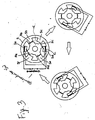
- the basic construction of the SR motor 1 is illustrated in Fig. 3.
- the motor 1 shown in Fig. 3 comprises a stator S, and a rotor R which is rotatably supported within the internal space of the stator S.
- the rotor R comprises a lamination of a number of thin iron sheets, and is formed with four outwardly projecting poles Ra to Rd at locations which are spaced apart by 90 degrees around its outer periphery.
- the stator S also comprises a lamination of a number of thin iron sheets, and is formed with six inwardly projecting six Sa to Sf at locations which are spaced apart by 60 degrees around its inner periphery.
- Each pole Sa to Sd of the stator S has an electrical coil CL disposed thereon.
- the coils CL each of which is disposed on the stator poles Sa and Sd respectively are denoted as phase 1 and denoted by reference character 1a in Fig. 1
- the coils each of which is disposed on the stator poles Sb and Se respectively are denoted as phase 2 and denoted by reference character 1b in Fig. 1
- the coils each of which is disposed on the stator poles Sc and Sf respectively are denoted as phase 3 and denoted by reference character 1c in Fig. 1.
- the coils CL (1a to 1c) By sequentially energising the coils CL (1a to 1c) in the sequence of phase 1-phase 2-phase 3 depending on the position of the poles on the rotor R, it is possible to drive the rotor R for continuous rotation in the clockwise direction.
- a pole on the stator S that is energised constitutes an electromagnet, and accordingly a pole on the rotor R which is located close to the electromagnet is attracted thereby for rotational movement.
- the coils that are energised may be switched in the sequence of phase 1-phase 2-phase 3 as the rotor R rotates through 30 degrees.
- the SR motor 1 is provided with three phase coils 1a, 1b, 1c which are used for driving the SR motor 1, and an angle sensor 1d which detects a rotation position or angle of rotation of the rotor R.
- the three phase coils 1a, 1b and 1c are connected to respective phase drivers 12, 13 and 14, respectively, which are contained in the controller ECU.
- a current sensor 2, 3 and 4 is provided between each of the respective phase drivers 12, 13 and 14 and the phase coils 1a, 1b and 1c.
- Each of these current sensors 2, 3 and 4 delivers a current signal S6 in the form of a voltage, which is proportional to an actual current flow through each of the coils 1a, 1b and 1c.
- the controller ECU contains a CPU (microcomputer) 5, an input interface 6, a current map memory 7, a power supply circuit 8, a current wave form generating circuit 9, a comparison circuit 10, an output decision circuit 11, and drivers 12, 13 and 14.
- the controller ECU sequentially calculates a driving speed (rotation number) on the basis of angle of rotation of the rotor R detected by the angle sensor 1d, and sequentially calculates a driving torque of the SR motor 1 on the basis of information which is fed from a shift lever, a brake switch, an accelerator switch and an accelerator opening sensor.
- the controller ECU controls the magnitude of current passed through each of the coils 1a, 1b and 1c of the motor 1 based on the results of such calculation.
- Fig. 2 specifically shows a main part of the circuit shown in Fig. 1. It is to be noted that Fig. 2 shows only the circuit which controls the energisation of phase 1 coil 1a, but it should be noted that similar circuits are employed for controlling the energisation of phase 2 and phase 3 coils 1b and 1c.
- phase 1 coil 1a has a first end connected through a first switching transistor IGBT 12a to a high potential line 12e of a direct current power supply while a second end of the coil 1a is connected through a second switching transistor IGBT 12b to a low potential line 12f of the power supply. Additionally, the first end of the phase 1 coil 1a is connected to the low potential line 12f through a diode 12c which allows a current flow from the latter to the former while the second end of the coil 1a is connected to the high potential line 12e through a diode 12d which allows a current flow from the former to the latter. Accordingly, when the transistors 12a and 12b are both turned on, a current flow is established from the power supply to the coil 1a. If either one or both of the transistors are turned off, the energisation of the coil 1a can be interrupted.
- the output decision circuit 11 includes AND gates 11a, 11b and 11c, a NOT gate 11d, a flip-flop circuit 11e, a NOR gate 11f.
- An output terminal of the NOR gate 11f is connected to a gate terminal of the first transistor 12a while an output terminal of the AND gate 11a is connected to a gate terminal of the second transistor 12b.
- Signals S72 and S5 are fed to an input terminal of the AND gate 11a while signals S8 and S9 are fed to an input terminal of the NOR gate 11f.
- the signal S72 is a binary signal delivered by a second analogue comparator 10b contained in the comparison circuit 10 while the signal S5 is a binary signal delivered by an AND gate 9i contained in the current wave form generating circuit 9.
- the signal S8 is a binary signal delivered by the NOT gate 11d while the signal S9 is a binary signal delivered by the flip-flop circuit 11e.
- the signal S8 as an input signal and a signal S12 as a reset signal are fed to the flip-flop circuit 11e.
- An output of the AND gate 11b is connected to an input of the NOT gate 11d while a signal S71 and the signals S72 and S5 are fed to an input of the AND gate 11b.
- the signal S71 is a binary signal delivered by a first analogue comparator 10a contained in the comparison circuit 10.
- the signal S12 is delivered by the AND gate 11c while a clock pulse signal S10 of 15 kHz and a signal S11 delivered by the current waveform generating circuit 9 are fed to an input of the AND gate 11c.
- the comparator 10 comprises the two analogue comparators 10a and 10b.
- the first analogue comparator 10a delivers a result of comparison between a first standard voltage Vr1 and a voltage Vs6 as a binary signal S71.
- the standard voltage Vr1 is an output of the current waveform generating circuit 9 while the voltage Vr6 is a voltage of the signal S6 corresponding to a current detected by the current sensor 2.
- the second analogue comparator 10b delivers a result of comparison between a second standard voltage Vr2 and the voltage Vs6 as a binary signal S72.
- the standard voltage Vr2 is another output of the current waveform generating circuit 9.
- the first standard voltage Vr1 is always smaller than the second standard voltage Vr2.
- the transistors 12a and 12b can adopt any of the following three conditions depending on the result of the comparison of the voltage Vs6 of the signal S6 and the first and second voltages Vr1 and Vr2: when the voltage Vs6 is smaller than the voltage Vr1, the signals S71 and S72 are both at a high level H, so that the outputs of the AND gates 11a and 11b are both at a high level H and the second transistor 12b is turned on. Meanwhile the output signal S8 of the NOT gate 11d is at a low level L.
- the output signal S9 of the flip-flop circuit 11e is not changed at the moment and maintained as a high level H until the signal S12 is turned to a high level H by the clock pulse signal S10.
- the output signal S9 is turned to a low level L, so that the output of the NOR gate 11f is turned to a high level H and the first transistor 12a is turned on.
- the voltage Vs6 is greater than the second standard voltage Vr2
- the signals S71 and S72 are both at a low level L, so that the outputs of the AND gates 11a and 11b are both at a low level L and the second transistor 12b is turned off.
- the output signal S8 of the NOT gate 11d is turned to a high level H, so that the output signal S9 of the flip-flop circuit 11e is turned to a high level on the basis thereof.
- the output of the NOR gate 11f is therefore turned to a low level L, so that the first transistor 12a is turned off.
- the signal S71 is at a low level L and the signal S72 is at a high level H, so that the output of the AND gate 11a is at a high level H and the second transistor 12b is turned on.
- the output of the AND gate 11b is at a low level L and the output signal S8 of the NOT gate 11d is at a high level H, so that the output signal S9 of the flip-flop circuit 11e is turned to a high level on the basis thereof.
- the output of the NOR gate 11f is therefore at a low level L, so that the first transistor 12a is turned off.
- the outputs of the AND gates 11a and 11b are always at a low level L irrespective of the output signals S71 and S72 of the comparison circuit 10, so that the second transistor 12b is turned off.
- the output signal S8 of the NOT gate 11d is at a high level, so that the output signal S9 of the flip-flop circuit 11e is turned to a high level on the basis thereof.
- the output of the NOR gate 11f is therefore at a low level L, so that the first transistor 12a is turned off. Namely, the transistors 12a and 12b are both turned off when the signal S5 is at a low level L.
- the transistors 12a and 12b can adopt any of the following three conditions depending on the result of the comparison of the voltage Vs6 of the signal S6 and the first and second voltages Vr1 and Vr2:
- the signals S71 and S72 are both at a high level H, so that the outputs of the AND gates 11a and 11b are both at a high level H and the second transistor 12b is turned on.
- the output signal S8 of the NOT gate 11d is at a low level L.
- the output signal S9 of the flip-flop circuit 11e is not changed at the moment.
- the output signal S12 of the AND gate 11c is always at a low level L, so that the flip-flop circuit 11e is not reset.
- the signals S71 and S72 are both at a low level L, so that the outputs of the AND gates 11a and 11b are both at a low level L and the transistor 12b is turned off.
- the output signal S8 of the NOT gate 11d is turned to a high level H, so that the output signal S9 of the flip-flop circuit 11e is turned to a high level on the basis thereof.
- the output of the NOR gate 11f is therefore turned to a low level L, so that the first transistor 12a is turned off.
- the signal S71 is at a low level L and the signal S72 is at a high level H, so that the output of the AND gate 11a is at a high level H and the second transistor 12b is turned on.
- the output of the AND gate 11b is at a low level L and the output signal S8 of the NOT gate 11d is at a high level H, so that the output signal S9 of the flip-flop circuit 11e is turned to a high level on the basis thereof.
- the output of the NOR gate 11f is therefore at a low level L, so that the first transistor 12a is turned off.
- the outputs of the AND gates 11a and 11b are always at a low level L irrespective of the output signals S71 and S72 of the comparison circuit 10, so that the second transistor 12b is turned off.
- the output signal S8 of the NOT gate 11d is at a high level, so that the output signal S9 of the flip-flop circuit 11e is turned to a high level on the basis thereof.
- the output of the NOR gate 11f is therefore at a low level L, so that the first transistor 12a is turned off. Namely, the transistors 12a and 12b are both turned off when the signal S5 is at a low level L.
- the voltage Vs6 is always smaller than the second standard voltage Vr2 since the difference between the first standard voltage Vr1 and the voltage Vs6 representing the current passing through the coil is not increased even if the fall speed of the current is slow. For the moment fluctuation different in current is small.
- the first and second standard voltages (target value of current) Vr1 and Vr2 are changed.
- the voltage Vs6 is greater than the second standard voltage Vr2 if the fall speed of current is slow. At that moment, the transistors 12a and 12b are both turned off, so that the fall speed of current is increased.
- JP03(1991)-049584 A shows advantage by the above turn-on/-off of either the two transistors which control the coil energisation in detail.
- the falling speed of the current is accelerated irrespective of a magnitude of the current (Vs6) by the manner in which the signal S5 is controlled.
- the transistors 12a and 12b are both turned off irrespective of the signals S71 and S72 when the signal is controlled to be changed at a low level L, so that the falling speed of current is accelerated.
- the iron loss of the SR motor is dependent on a maximum number of the magnetic flux of each coil during energisation and the number of the magnetic flux is the greatest at the current fall.
- the maximum number of the magnetic flux is reduced by controlling the energisation of the coils although a conventional motor is used. Since the quantity of the magnetic flux is increased while the transistors 12a and 12b are turned on, the term for which the transistors are turned on is shortened as much as possible. Furthermore when the current is falling, the current fall process is started by turning off one of the transistors 12a and 12b first so that an increase in the magnetic flux is avoided and then the current fall is completed by turning both of the transistors 12a and 12b off. Therefore this embodiment makes it possible to reduce the maximum number of the magnetic flux by the above control.
- the current waveform generating# circuit 9 outputs the first and second standard voltages Vr1 and Vr2 and the binary signals S5 and S11.
- the standard voltages Vr1 and Vr2 and the binary signals S5 and S11 are generated on the basis of information stored in the memories (RAM) 9b, 9a, 9c and 9d respectively.
- the memory 9a, 9b, 9c and 9d comprises 8-bit, 8-bit, 1-bit and 1-bit data in each address.
- the 8-bit data read from the memory 9a is converted to an analogue voltage by a D/A (Digital/analogue) converter 9e passed through an amplifier 9g to give the standard voltage Vr2.
- D/A Digital/analogue
- the 8-bit data read from the memory 9b is also converted to an analogue voltage by a D/A converter 9f and passed through an amplifier 9h to give the standard voltage Vr1.
- An analogue signal S1 outputted from the CPU 5 is also input to the amplifiers 9g and 9h respectively.
- the standard voltages are exactly adjusted respectively by adjusting the amplitude of the signal S1.
- the 1-bit data outputted from the memory 9c is input to an AND gate 9i to produce the signal S5.
- a binary signal (start/stop signal) S3 outputted from the CPU 5 is added to another input terminal of the AND gate 9i. While the SR motor 1 is driven, the signal S3 is always at a high level H, so that the binary signal S5 is dependent on the output signal of the memory 9c.
- the 1-bit data outputted from the memory 9d is directly used as the signal S11.
- the memories 9a, 9b, 9c and 9d comprises a plurality of addresses respectively and each address corresponds to each angle (each 1 degree) of rotation of the rotor R.
- An address decoder 9j generates address information on the basis of the signal S13 representing the angle of rotation of the rotor R detected by the angle sensor 1d. The address information is fed to address input terminals of the memories 9a, 9b, 9c and 9d at the same time respectively. While the SR motor is driven and the rotor R rotates, the memories 9a, 9b, 9c and 9d output data stored in address corresponding to each of angle of rotation of the rotor R.
- the status of the standard voltage Vr1 and Vr2 and the binary signals S5 and S11 could be different with respect to the angle of rotation of the rotor R.
- the memories 9a and 9b comprises information of energising map shown in Fig. 8 respectively so as to supply the current waveform in Fig. 4 to the three phase coils.
- a target value for current to be supplied at each angle of rotation is comprised in each address corresponding to each angle of rotation (each 0.5 degree in this embodiment).
- Information of memories 9a and 9b are corresponding to the standard voltage Vr1 and Vr2 respectively, so that the contents of the memory 9a is somewhat different from that of the memory 9b so as to satisfy the relation that the voltage Vr2 is greater than the voltage Vr1.
- the current supplied to the coil 1a is varied to follow the first standard voltage Vr1.
- the current is supplied as shown in Fig. 4 since the current waveform to be supplied to the coil 1a is registered as the standard voltage Vr1 and Vr2 in memories 9a and 9b.
- Most of its addresses comprises information "1" corresponding to a high level H for the signal S5, however addresses corresponding to angles where the target value (Vr1, Vr2) is suddenly reduced comprise information "0" (compulsory switch off information) corresponding to a low level L for the signal S5.
- the signal S5 is turned to a low level L on the basis of information in the memory 9c so that the fall speed of the current undergoes compulsory acceleration at an angle of rotation when such an acceleration is desirable and when the target value (Vr1, Vr2) of the current drops suddenly. Therefore, time delay is prevented and the current matches the target value more closely.
- Memory 9d contains addresses for controlling the switching of transistor 12a.
- the addresses comprising "0" correspond to a low level L for the signal S11 which turns off the transistor 12a.
- the other addresses comprising "1" correspond to a high level H for the signal S11. It is possible to read and write the data at memories 9a, 9b, 9c and 9d respectively all of which are processed at the same time.
- the memories 9a, 9b, 9c and 9d are connected with CPU 5 via a signal line S2 and the CPU 5 refreshes the contents of the memories 9a, 9b, 9c and 9d as the need arises.
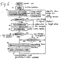
- FIG.6 A control operation performed by CPU 5 shown in Figs. 1 and 2 is schematically indicated in Fig.6.
- CPU 5 executes an initialisation at step 61.
- internal memories within CPU 5 are initialised, internal timers and an interrupt mode are set up, followed by a system diagnosis. If no abnormality is found, the operation proceeds to the next step.
- step 62 the status of signals delivered from the shift lever, brake switch, accelerator switch and accelerator opening sensor are read through the input interface 6 and the status is stored in an internal memory. If any change in the status is detected at step 62, the operation proceeds to step 64 through step 63. Otherwise, the operation proceeds to step 65 through step 63.
- a target value of the driving torque of the SR motor 1 is determined on the basis of various status detected at step 62. For example, when the accelerator opening sensor has detected an increased accelerator opening, a target value of the driving torque is also increased.
- a torque change flag indicating that there has been a change in the target torque, is set.
- step 65 the current rotational speed of the SR motor 1 is detected and stored in the internal memory.
- step 66 the operation proceeds from step 66 to step 68. If there is no change in the rotational speed, the operation proceeds from step 66 to step 67 where the status of the torque change flag is examined, and when it is set, indicating that there has been a change in the target torque, the operation proceeds to step 68. When there is no change in the torque, the operation returns to step 62.
- map memory 7 is accessed to read data therefrom, at step 69, energisation map is generated, and data is updated.
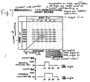
- the map memory 7 is a read-only memory having a variety of data pre-stored therein. Several groups of data stored in the memory 7 are shown in Fig. 7.
- the map memory 7 contains a multiplicity of data items Cnm, (where n represents a column number corresponding to the torque, and m represents a row number corresponding to the number of revolutions) corresponding to the target torque and numbers of revolution of the SR motor 1 respectively.
- a set of the data Cnm comprises a first energisation off angle, a second energisation off angle and a target value of the current.
- data item C34 contains 44.0 degrees, 58.0 degrees, 66.0 degrees and 300 A when the target torque is 30 Nm and the rotation speed is 6000 rpm.
- a coil is energised by a current of 300 A from 44.0 to 58.0 degrees, one of the transistors (12a,12b) is turned off from 58.0 to 66.0 degrees so as to deenergise the coil (current is not supplied from power supply).
- the coil is not energised from 0 to 43.95 degrees and from 66.05 to 90.0 degrees.
- a set of data Cnm selected on the basis of a torque and revolution speed at a time is fed.
- Fig. 5a shows changes of the current waveform, torque waveform and flux linkage controlled by conventional manner. Namely an energisation on angle, an energisation off angle and a target value corresponding to an angle of rotation are determined with respect to the coil 1a on the basis of a target torque and a rotation speed, the transistors (switching elements) 12a and 12b are both turned on when the energisation on angle is reached, the transistor 12a is turned off if a value of an actual current is over the target value of the current while the energisation off angle has not been reached and the transistors 12a and 12b are both turned off when the energisation off angle is reached. As shown in Fig. 5a, in the section between the energisation on and off angles, flux linkage increases when the transistors 12a and 12b are both turned on and is continued until the transistors 12a and 12b are both turned off.
- Fig. 5b shows changes of the current waveform, torque waveform and flux linkage controlled by the embodiment of the invention. Namely an energisation on angle, a first energisation off angle, a second energisation off angle and a target value corresponding to an angle of rotation are determined with respect to the coil 1a on the basis of a target torque and a rotation speed, the transistors (switching elements) 12a and 12b are both turned on when the energisation on angle is reached, the first transistor 12a is turned off if a value of an actual current is over the target value of the current while the first energisation off angle has not been reached, the transistor 12a is turned off irrespective of the magnitude of the value of the actual current and the target value of the current when the first energisation off angle is reached and both transistors 12a and 12b are turned off when the second energisation off angle is reached.
- means for controlling the energisation of the embodiment controls as follows:
- a target torque is determined for the SR motor on the basis of information fed from means for detecting an angle of rotation of a rotor, means for detecting a rotation speed of the rotor, means for detecting an actual current passing through each phase coil.
- An energisation on angle, a first and a second energisation off angle and a target value of a current are determined with respect to each coil on the basis of a target torque and a rotation speed.
- the first and second switching elements are both turned off when the angle of rotation is within a section from the second energisation off angle to the energisation on angle.
- the actual value of the current is approximated to the target value by means of alternate repeat that either the first and second switching element is turned on the other is turned off and the first and second switching element are both turned on when the angle of rotation is within a section from the energisation on angle to the first energisation off angle. Either the first and second switching element is turned on the other is turned off when the angle of rotation is within a section from the first to second energisation off angles.
Landscapes
- Engineering & Computer Science (AREA)
- Power Engineering (AREA)
- Control Of Electric Motors In General (AREA)
Applications Claiming Priority (2)
| Application Number | Priority Date | Filing Date | Title |
|---|---|---|---|
| JP8343898 | 1998-03-30 | ||
| JP8343898 | 1998-03-30 |
Publications (2)
| Publication Number | Publication Date |
|---|---|
| EP0948125A2 true EP0948125A2 (de) | 1999-10-06 |
| EP0948125A3 EP0948125A3 (de) | 2001-02-14 |
Family
ID=13802442
Family Applications (1)
| Application Number | Title | Priority Date | Filing Date |
|---|---|---|---|
| EP99302649A Withdrawn EP0948125A3 (de) | 1998-03-30 | 1999-03-30 | Erregungssteuerung für einen geschalteten Reluktanzmotor |
Country Status (2)
| Country | Link |
|---|---|
| US (1) | US6157160A (de) |
| EP (1) | EP0948125A3 (de) |
Cited By (1)
| Publication number | Priority date | Publication date | Assignee | Title |
|---|---|---|---|---|
| EP1067670A3 (de) * | 1999-07-05 | 2001-09-26 | Nissan Motor Company, Limited | Regelungsverfahren für einen geschalteten Reluktanzmotor und Reluktanzmotor mit geringem Spitzenstrom |
Families Citing this family (7)
| Publication number | Priority date | Publication date | Assignee | Title |
|---|---|---|---|---|
| US6472842B1 (en) * | 1997-10-03 | 2002-10-29 | The Texas A&M University System | Self-tuning control of switched-reluctance motor drive system |
| EP1256164A2 (de) * | 2000-02-09 | 2002-11-13 | Dana Corporation | Steuerungsverfahren für einen reluktanzgenerator |
| JP4055882B2 (ja) * | 2000-08-31 | 2008-03-05 | 株式会社小松製作所 | ソレノイド駆動装置 |
| US7265516B2 (en) * | 2001-12-13 | 2007-09-04 | Lacroix Michael Charles | Linear electric motor controller and system for providing linear control |
| TW200402929A (en) * | 2002-07-22 | 2004-02-16 | Switched Reluctance Drives Ltd | Control of a switched reluctance drive |
| JP4187565B2 (ja) * | 2003-03-28 | 2008-11-26 | 株式会社モリテックス | 照明装置 |
| US9198500B2 (en) | 2012-12-21 | 2015-12-01 | Murray W. Davis | Portable self powered line mountable electric power line and environment parameter monitoring transmitting and receiving system |
Family Cites Families (9)
| Publication number | Priority date | Publication date | Assignee | Title |
|---|---|---|---|---|
| US4710686A (en) * | 1986-08-04 | 1987-12-01 | Guzik Technical Enterprises | Method and apparatus for control of current in a motor winding |
| US4879641A (en) * | 1987-11-02 | 1989-11-07 | Sgs-Thomson Microelectronics S.R.L. | Analog multiplex for sensing the magnitude and sense of the current through a h-bridge stage utilizing a single sensing resistance |
| FR2702104B1 (fr) * | 1993-02-23 | 1995-06-30 | Aerospatiale | Procede de pilotage d'un appareil electrique reversible. |
| US5446359A (en) * | 1993-12-29 | 1995-08-29 | Emerson Electric Co. | Current decay control in switched reluctance motor |
| JPH07274570A (ja) * | 1994-03-31 | 1995-10-20 | Aisin Seiki Co Ltd | スイッチドレラクタンスモ−タの制御装置 |
| JP3268573B2 (ja) * | 1994-04-25 | 2002-03-25 | アイシン精機株式会社 | スイッチドレラクタンスモ−タの制御装置 |
| US5801504A (en) * | 1995-09-25 | 1998-09-01 | Nsk Ltd. | Control apparatus for electric power steering system |
| US5744922A (en) * | 1996-09-16 | 1998-04-28 | Xerox Corporation | Current regulator |
| JP3826499B2 (ja) * | 1997-06-27 | 2006-09-27 | アイシン精機株式会社 | 電気モータの通電制御装置 |
-
1999
- 1999-03-30 EP EP99302649A patent/EP0948125A3/de not_active Withdrawn
- 1999-03-30 US US09/280,701 patent/US6157160A/en not_active Expired - Fee Related
Cited By (2)
| Publication number | Priority date | Publication date | Assignee | Title |
|---|---|---|---|---|
| EP1067670A3 (de) * | 1999-07-05 | 2001-09-26 | Nissan Motor Company, Limited | Regelungsverfahren für einen geschalteten Reluktanzmotor und Reluktanzmotor mit geringem Spitzenstrom |
| US6469468B1 (en) | 1999-07-05 | 2002-10-22 | Nissan Motor Co., Ltd. | SR motor controlling method and SR motor having low peak of current flowing therein |
Also Published As
| Publication number | Publication date |
|---|---|
| EP0948125A3 (de) | 2001-02-14 |
| US6157160A (en) | 2000-12-05 |
Similar Documents
| Publication | Publication Date | Title |
|---|---|---|
| JP3268573B2 (ja) | スイッチドレラクタンスモ−タの制御装置 | |
| JPH0998594A (ja) | 電気モ−タの通電制御方法 | |
| US5532567A (en) | Controller for switched reluctance motor | |
| US5754024A (en) | Control device for switched reluctance motor | |
| US6153956A (en) | Switched reluctance position sensing | |
| US6157160A (en) | Energization control of a switched reluctance motor | |
| US5537019A (en) | Switched reluctance motor providing rotor position detection at high speeds without a separate rotor shaft position sensor | |
| US5786673A (en) | Electric motor | |
| JP3803781B2 (ja) | 電気モ−タの通電制御装置 | |
| JPH07274569A (ja) | 電気モ−タの通電制御装置 | |
| US5999431A (en) | Power controller for a switched reluctance motor with a high frequency noise filter | |
| JP3801731B2 (ja) | 電気モ−タの通電制御装置 | |
| JP3700106B2 (ja) | センサレス・スイッチドリラクタンスモータの駆動回路 | |
| JP3564582B2 (ja) | スイッチドレラクタンスモ−タの通電制御装置 | |
| JP3381107B2 (ja) | チョッピング通電制御装置 | |
| US5959419A (en) | Energization controller of electric motor | |
| CN101019304A (zh) | 用于最优化电机的励磁电流波形轮廓的自适应系统 | |
| JPH11136984A (ja) | スイッチドリラクタンスモータの通電制御装置 | |
| JP2002281784A (ja) | モータの駆動制御装置 | |
| JPH11346494A (ja) | 電気モ―タの通電制御装置 | |
| JP3256840B2 (ja) | ブラシレスモータの駆動制御装置 | |
| JP3406995B2 (ja) | チョッピング通電制御装置 | |
| JPH0648916B2 (ja) | 電動機の速度制御装置 | |
| JP3416684B2 (ja) | 電気モ−タの通電制御装置 | |
| JPH10243682A (ja) | モータ駆動制御装置における制御方法 |
Legal Events
| Date | Code | Title | Description |
|---|---|---|---|
| PUAI | Public reference made under article 153(3) epc to a published international application that has entered the european phase |
Free format text: ORIGINAL CODE: 0009012 |
|
| AK | Designated contracting states |
Kind code of ref document: A2 Designated state(s): DE FR GB |
|
| AX | Request for extension of the european patent |
Free format text: AL;LT;LV;MK;RO;SI |
|
| RIN1 | Information on inventor provided before grant (corrected) |
Inventor name: MA, XIAOOU Inventor name: FUKUSHIMA, TOMOHIRO Inventor name: KITAMURA, YUICHIRO Inventor name: OKAWA, AKEMI |
|
| PUAL | Search report despatched |
Free format text: ORIGINAL CODE: 0009013 |
|
| AK | Designated contracting states |
Kind code of ref document: A3 Designated state(s): AT BE CH CY DE DK ES FI FR GB GR IE IT LI LU MC NL PT SE |
|
| AX | Request for extension of the european patent |
Free format text: AL;LT;LV;MK;RO;SI |
|
| RIC1 | Information provided on ipc code assigned before grant |
Free format text: 7H 02P 5/05 A, 7H 02P 7/05 B |
|
| 17P | Request for examination filed |
Effective date: 20010312 |
|
| AKX | Designation fees paid |
Free format text: DE FR GB |
|
| STAA | Information on the status of an ep patent application or granted ep patent |
Free format text: STATUS: THE APPLICATION HAS BEEN WITHDRAWN |
|
| 18W | Application withdrawn |
Effective date: 20060131 |