EP0949604A1 - Zweidimensionale Anordnung lichtemittierender Elemente und Ansteuermethoden dafür - Google Patents
Zweidimensionale Anordnung lichtemittierender Elemente und Ansteuermethoden dafür Download PDFInfo
- Publication number
- EP0949604A1 EP0949604A1 EP99302763A EP99302763A EP0949604A1 EP 0949604 A1 EP0949604 A1 EP 0949604A1 EP 99302763 A EP99302763 A EP 99302763A EP 99302763 A EP99302763 A EP 99302763A EP 0949604 A1 EP0949604 A1 EP 0949604A1
- Authority
- EP
- European Patent Office
- Prior art keywords
- level
- driving
- light
- element array
- column
- Prior art date
- Legal status (The legal status is an assumption and is not a legal conclusion. Google has not performed a legal analysis and makes no representation as to the accuracy of the status listed.)
- Withdrawn
Links
- 238000000034 method Methods 0.000 title claims description 12
- 239000011159 matrix material Substances 0.000 claims abstract description 56
- 239000000463 material Substances 0.000 claims description 8
- 238000009792 diffusion process Methods 0.000 description 3
- 229910001218 Gallium arsenide Inorganic materials 0.000 description 2
- 150000001875 compounds Chemical class 0.000 description 2
- 230000001603 reducing effect Effects 0.000 description 2
- 239000004065 semiconductor Substances 0.000 description 2
- XUIMIQQOPSSXEZ-UHFFFAOYSA-N Silicon Chemical compound [Si] XUIMIQQOPSSXEZ-UHFFFAOYSA-N 0.000 description 1
- 238000003491 array Methods 0.000 description 1
- 239000000969 carrier Substances 0.000 description 1
- 238000003776 cleavage reaction Methods 0.000 description 1
- 230000004048 modification Effects 0.000 description 1
- 238000012986 modification Methods 0.000 description 1
- 230000010355 oscillation Effects 0.000 description 1
- 238000005215 recombination Methods 0.000 description 1
- 230000006798 recombination Effects 0.000 description 1
- 230000007017 scission Effects 0.000 description 1
- 229910052710 silicon Inorganic materials 0.000 description 1
- 239000010703 silicon Substances 0.000 description 1
- 239000000758 substrate Substances 0.000 description 1
Images




Classifications
-
- G—PHYSICS
- G09—EDUCATION; CRYPTOGRAPHY; DISPLAY; ADVERTISING; SEALS
- G09G—ARRANGEMENTS OR CIRCUITS FOR CONTROL OF INDICATING DEVICES USING STATIC MEANS TO PRESENT VARIABLE INFORMATION
- G09G3/00—Control arrangements or circuits, of interest only in connection with visual indicators other than cathode-ray tubes
- G09G3/20—Control arrangements or circuits, of interest only in connection with visual indicators other than cathode-ray tubes for presentation of an assembly of a number of characters, e.g. a page, by composing the assembly by combination of individual elements arranged in a matrix no fixed position being assigned to or needed to be assigned to the individual characters or partial characters
- G09G3/22—Control arrangements or circuits, of interest only in connection with visual indicators other than cathode-ray tubes for presentation of an assembly of a number of characters, e.g. a page, by composing the assembly by combination of individual elements arranged in a matrix no fixed position being assigned to or needed to be assigned to the individual characters or partial characters using controlled light sources
- G09G3/30—Control arrangements or circuits, of interest only in connection with visual indicators other than cathode-ray tubes for presentation of an assembly of a number of characters, e.g. a page, by composing the assembly by combination of individual elements arranged in a matrix no fixed position being assigned to or needed to be assigned to the individual characters or partial characters using controlled light sources using electroluminescent panels
- G09G3/32—Control arrangements or circuits, of interest only in connection with visual indicators other than cathode-ray tubes for presentation of an assembly of a number of characters, e.g. a page, by composing the assembly by combination of individual elements arranged in a matrix no fixed position being assigned to or needed to be assigned to the individual characters or partial characters using controlled light sources using electroluminescent panels semiconductive, e.g. using light-emitting diodes [LED]
-
- G—PHYSICS
- G09—EDUCATION; CRYPTOGRAPHY; DISPLAY; ADVERTISING; SEALS
- G09G—ARRANGEMENTS OR CIRCUITS FOR CONTROL OF INDICATING DEVICES USING STATIC MEANS TO PRESENT VARIABLE INFORMATION
- G09G2300/00—Aspects of the constitution of display devices
- G09G2300/08—Active matrix structure, i.e. with use of active elements, inclusive of non-linear two terminal elements, in the pixels together with light emitting or modulating elements
Definitions
- the present invention generally relates to a two-dimensional light-emitting element array device, particularly to a two-dimensional light-emitting element array device using three-terminal light-emitting thyristors.
- the present invention further relates to a method for driving such a two-dimensional light-emitting element array device.
- a two-dimensional light-emitting element array device constituted by arranging a plurality of three-terminal thyristors of PNPN structure in two-dimension have been disclosed in Japanese Patent Publication Nos. 3-200364 and 3-273288, these publications being related to the Japanese Patent applications filed by the present applicant.
- the two-dimensional light-emitting array device disclosed in these publications needs at least three light-emitting thyristors and three clock lines for constituting one picture-element, so that there is such a problem that the area of one picture-element is large.
- Fig. 1 shows the two-dimensional light-emitting element array device disclosed in Japanese Patent Publication No.3-273288.
- a plurality of light-emitting thyristors are arranged in two-dimension, i.e., in X-Y matrix.
- Clock lines CK 1 - CK 3 which supply clocks ⁇ 1 - ⁇ 3 respectively are connected to the thyristor in such a way that each clock line is connected obliquely from the thyristor on upper left to the thyristor on lower right.
- ON state (light-on state) of the light-emitting thyristor P may be transferred on the device toward the right side or lower side on the drawing.
- four light-emitting thyristors enclosed by a dotted-line 10 constitutes one picture-element. Therefore, the area of one picture-element is large, resulting in the low density of picture-elements.
- the object of the present invention is to provide a two-dimensional light-emitting element array device in which the density of picture-elements may be increased.
- Another object of the present invention is to provide a method for driving the two-dimensional light emitting element array device.
- a two-dimensional light-emitting element array device comprises a light-emitting element array in which a plurality of three-terminal light-emitting thyristors are arranged in X-Y matrix of N rows ⁇ M columns (N ⁇ 1, M ⁇ 0) ; a plurality of row lines to each thereof an anode of the thyristor on a corresponding row of the matrix is connected ; one clock line to which all the row lines are connected ; a plurality of row address lines to each thereof a gate of the thyristor on a corresponding row and a 0th column of the matrix is connected ; and a plurality of column address lines to each thereof a gate of the thyristor on a corresponding column of 1st-Mth columns of the matrix is connected ; and light-emitting portions of all the thyristors on the 0th column are covered by an opaque material.
- a method for driving this device in such a manner that one or more thyristors on a Jth column (1 ⁇ J ⁇ M) of the matrix is intended to emit light comprises the steps of : driving a row address line to High-level, which is of a corresponding row of the matrix on which a thyristor to be emitted light is, while driving other row address lines to Low-level ; driving a column address line on the Jth column to Low-level, while driving other column address lines to High-level ; and driving the clock line to High-level.
- a two-dimensional light-emitting element array device comprises a light-emitting element array in which a plurality of three-terminal light-emitting thyristors are arranged in X-Y matrix of N rows ⁇ M columns (N ⁇ 1, M ⁇ 1) ; one clock line to which anodes of all the thyristors are connected ; a plurality of row address lines to each thereof a gate of the thyristor on a corresponding row of the matrix is connected through a first resistor ; and a plurality of column address lines to each thereof a gate of the thyristor on a corresponding column of the matrix is connected through a second resistor.
- a method for driving this device in such a manner that a thyristor on a Ith row and Jth column (1 ⁇ I ⁇ N, 1 ⁇ J ⁇ M) of the matrix is intended to emit light comprises the steps of : driving a row address line on the Ith row to Low-level, while driving other row address lines to High-level ; driving a column address line of the Jth column to Low-level, while driving other column address lines to High-level ; and driving the clock line to High-level.
- a two-dimensional light-emitting element array device comprises a light-emitting element array in which a plurality of three-terminal light-emitting thyristors are arranged in X-Y matrix of N rows ⁇ M columns (N ⁇ 1, M ⁇ 0) ; a plurality of row lines to each thereof an anode of the thyristor on a corresponding row of the matrix is connected ; one clock line to which all the row lines are connected ; a plurality of row address lines to each thereof a gate of the thyristor on a corresponding row and a 0th column of the matrix is connected ; a plurality of column address lines to each thereof a gate of the thyristor on a corresponding column of 1st-Mth columns of the matrix is connected ; a first self-scanning type transfer element array for driving the column address lines to High-level or Low-level by self scanning thereof ; and a second self-scanning type transfer
- a method for driving this device in such a manner that one or more thyristors on a Jth column (1 ⁇ J ⁇ M) of the matrix is intended to emit light comprises the steps of : driving the column address lines in turn to High-level by the first self-scanning type transfer element array ; driving one or more row address lines to High-level, while driving other row address lines to Low-level by the second self-scanning type transfer element array, when the column address line on the Jth column is driven to Low-level; and driving the clock line to High-level.
- a two-dimensional light-emitting element array device comprises a light-emitting element array in which a plurality of three-terminal light-emitting thyristors are arranged in X-Y matrix of N rows ⁇ M columns (N ⁇ 1, M ⁇ 1) ; one clock line to which anodes of all the thyristors are connected ; a plurality of row address lines to each thereof a gate of the thyristor on a corresponding row of the matrix is connected through a first resistor ; a plurality of column address lines to each thereof a gate of the thyristor on a corresponding column of the matrix is connected through a second resistor ; a first-scanning type transfer element array for driving the column address lines to High-level or Low-level by self scanning thereof ; and a second-scanning type transfer element array for driving the row address lines to High-level or Low-level by self scanning thereof.
- a method for driving this device in such a manner that a thyristor on a Ith row and Jth column (1 ⁇ I ⁇ N, 1 ⁇ J ⁇ M) of the matrix is intended to emit light comprises the steps of : driving the column address lines in turn to Low-level by the first self-scanning type transfer element array ; driving the row address lines in turn to Low-level by the second self-scanning type transfer element array, when the column address line on the Jth column is driven to Low-level ; and driving the clock line to High-level.
- the density of picture-elements of the device may be increased, since one light-emitting thyristor constitutes one picture-element.
- Fig.1 shows a conventional two-dimensional light-emitting element array device.
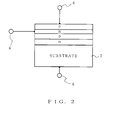
- Fig.2 shows a fundamental structure of a three-terminal light-emitting thyristor.
- Fig.3 shows a first embodiment of the two-dimensional light-emitting element array device of the present invention.
- Fig.4 shows a second embodiment of the two-dimensional light-emitting element array device of the present invention.
- Fig.5 shows a third embodiment of the two-dimensional light-emitting element array device of the present invention.
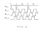
- Fig.6 shows exemplary driving pulses for a three-phase driving self-scanning type transfer element array.
- Fig.7 shows a fourth embodiment of the two-dimensional light-emitting element array device of the present invention.
- LED Light-Emitting Diode
- LD Laser Diode
- LED constitutes a PN or PIN junction by compound semiconductor such as GaAs, GaP, GaAlAs, and the like, and utilizes a light-emitting phenomenon based on the recombination of carriers injected into the junction to which a forward voltage is applied.
- LD has a structure in which a waveguide is provided in LED.
- a current larger than a threshold current flows into LD, electron-hole pairs are increased to arise population inversion.
- the multiplication of photon due to a stimulated emission is occurred to generate light by means of parallel reflecting mirrors formed by cleavage planes.
- the light is again fed back to an active layer to cause a laser oscillation, and a laser is emitted from the end surface of the wave guide.
- a negative-resistance element (a light-emitting thyristor, a laser thyristor, and the like) which has same light-emitting mechanism as that of LED and LD.
- the light-emitting thyristor constitutes a PNPN structure with compound semiconductor, and is commercially available as a silicon thyristor.
- Fig.2 shows a fundamental structure of a three-terminal light-emitting thyristor.
- a PNPN structure is formed on an N-type GaAs substrate 2.
- the thyristor has three terminals, i.e., a gate 4, an anode 6, and a cathode 8.
- the gate 4 serves for controlling an ON voltage, i.e., a turn-on voltage applied to the anode 6.
- the ON voltage is equal to the voltage, i.e., the sum of a diffusion potential of the PN junction and a voltage drop due to a current necessary for turning-on the thyristor.
- the voltage of the gate 4 becomes substantially equal to the voltage of the cathode 8. Therefore, if the cathode 8 is connected to the ground, then the gate voltage becomes 0 volt.
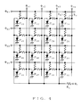
- Fig.3 shows a first embodiment of the two-dimensional light-emitting element array device according to the present invention.
- This device comprises a light-emitting element array in which a plurality of three-terminal light-emitting thyristors are arranged in two-dimension, i.e., in an X-Y matrix of N rows ⁇ M columns (N ⁇ 1, M ⁇ 0).
- N ⁇ 1, M ⁇ 0 the matrix of 4 ⁇ 5 is shown for simplicity of the drawing.
- the anodes of the thyristors on the Ith row (1 ⁇ I ⁇ N) of the matrix are connected to a corresponding row line 12 of the Ith row.
- Each row line 12 is connected to a clock line ⁇ 1 , through a corresponding resistor R L1 , R L2 , R L3 , ••• as shown in the figure.
- the gates of the thyristors on the Jth column (1 ⁇ J ⁇ M) of the matrix are connected to a corresponding column address line ⁇ v1 , ⁇ v2 , ⁇ v3 , •••, respectively.
- the gates of the thyristors P 10 , P 20 , P 30 , ••• on the 0th column are connected to a corresponding row address lines ⁇ h1 , ⁇ h2 , ⁇ h3 , •••, respectively.
- the cathodes of all the thyristors are connected to the ground.
- Light-emitting portions of all the thyristors P 10 , P 20 , P 30 , ••• on the 0th column are covered by an opaque material (not shown) in order to prevent the emitted light from leaking to the surface of the device.
- the thyristor having the lowest gate voltage may emit light at the beginning.
- the gate voltage thereof goes to the voltage of the cathode, i.e., 0 volt
- the anode voltage thereof substantially equals to a diffusion voltage of the PN junction.
- the voltage of the row line 12 is fixed to said anode voltage. Therefore, other thyristors connected to the same row line 12 may not turn-on even if the gate voltage thereof goes to Low-level i.e., 0 volt.
- the thyristor P I0 on the 0th column will preferentially emit light when the clock line ⁇ I is driven to High-level.
- the thyristor will emit light to which the Jth column address line ⁇ vJ driven to Low-level is connected.
- any thyristor on the Jth column of the matrix is caused to emit light.
- the 1st-Nth row address lines are driven to High-level or Low-level, respectively, according to light-emission information.
- the Jth column address line ⁇ vJ selected by scanning is driven to Low-level, and the column address lines other than the column address line ⁇ vJ are driven to High-level.
- the clock line ⁇ I is driven to High-level.
- the thyristor P IJ on the Ith row and Jth column of the matrix emits light
- the thyristor P I0 covered by the opaque material on the Ith row and 0th column emits light.
- Fig.4 shows a second embodiment of the two-dimensional light-emitting element array device according to the present invention.
- This device comprises a light-emitting element array in which a plurality of three-terminal light-emitting thyristor are arranged in an X-Y matrix of N rows ⁇ M columns (N ⁇ 1, M ⁇ 1). In the figure, the matrix of 4 ⁇ 4 is shown for simplicity of the drawing.
- anodes of all the thyristors are connected together to a clock line ⁇ I through a resistor R L .
- the gate of the thyristor P IJ on the Ith row and Jth column (1 ⁇ I ⁇ N, 1 ⁇ J ⁇ M) of the matrix is connected to a row address line ⁇ hI of the Ith row through a resistor R h , and to a column address line ⁇ vJ of the Jth column through a resistor R v .
- the gate voltage of the thyristor P IJ is equal to the mean value of both the voltage of the Ith row address line ⁇ hI and the voltage of the Jth column address line ⁇ hJ , if the values of two resistors R h , R v are selected to be equal. Therefore, when both the Ith row address line ⁇ hI and the Jth column address line ⁇ vJ are driven to Low-level and other row address lines and column address lines are driven to High-level, the gate voltage of the thyristor P IJ goes to the lowest voltage such as 0 volt. Therefore, when the clock line ⁇ I is driven to High-level, the thyristor P IJ emits light and other thyristors do not emit light. In this manner, only one thyristor may emit light among the thyristors arranged in the X-Y matrix at the same time.
- Fig.5 shows a third embodiment of the two-dimensional light-emitting element array device according to the present invention.
- This device comprises a light-emitting element array of N ⁇ M matrix which is same as the array shown in Fig.3., a three-phase driving self-scanning type transfer element array 16 for driving the row address lines ⁇ h1 , ⁇ h2 , ⁇ h3 , ••• of the light-emitting element array, and a two-phase driving self-scanning type transfer element array 18 for driving the column address lines ⁇ v1 , ⁇ v2 , ⁇ v3 , ••• of the light-emitting element array.
- These self-scanning type transfer element array 16 and 18 are the same type of array as disclosed in Japanese Patent No. 2577034 issued to the present applicant, the content of this Japanese patent being incorporated herein by reference.
- the three-phase driving self-scanning type transfer element array 16 a plurality of transfer elements connected to the same transfer clock line may be turned-on at the same time.
- the two-phase driving self-scanning type transfer element array 18 only one transfer element connected to the same transfer clock line may be turned-on at the same time.
- Transfer elements T v1 , T v2 , T v3 , ••• each thereof consisting of a three-terminal light-emitting thyristor are arranged in one dimension, i.e., in X-direction.
- the gates of adjacent transfer elements are interconnected through a diode D .
- Each gate of the transfer element is connected to a supply voltage ⁇ GA through a corresponding load resistor R .
- the gate of the first transfer element T v1 is connected to a start pulse line ⁇ vS .
- Respective anodes of the transfer elements are alternately connected to two-phase transfer clock lines ⁇ vc1 , ⁇ vc2 .
- Respective cathodes of the transfer elements are connected to the ground. Since the transfer elements consist of light-emitting thyristors, light-emitting portion thereof must be covered by an opaque material so that light does not come through to the surface of the device.
- Each gate of transfer elements in the array 18 is also connected to a corresponding column address line of the Jth column (1 ⁇ J ⁇ M) of the light-emitting element array.
- the gate voltage of this transfer element is reduced from the supply voltage ⁇ GA , e.g., 5 volts to about 0 volt.
- the voltage reducing effect works to the gate of the adjacent transfer element T v(J+1) on the right, setting the voltage of that gate to about 1 volt, i.e., a forward rise voltage of the thyristor.
- the voltage reducing effect does not work to the gate of the adjacent transfer element T v(J-1) on the left, because the diode D is reverse-biased.
- the turn-on voltage of the transfer elements is approximated to the gate voltage plus the diffusion potential of the PN junction (about 1 volt). Therefore, if the voltage of the transfer clock line ⁇ vc2 is set to the voltage which is higher than about 2 volts which is necessary voltage for turning-on the transfer element T v(J+1) and lower than about 4 volts which is necessary voltage for turning-on the transfer element T v(J+3 ), only the transfer element T v(J+1) may be turned-on while keeping other transfer elements turned-off. Thus, ON state may be transferred by setting alternately the voltages of the two transfer clock lines ⁇ vc1 and ⁇ vc2 to High-level.
- the structure of the three-phase driving self-scanning type transfer element array 16 is essentially the same as that of the two-phase driving self-scanning type transfer element array 18, except that the transfer clock lines are three-phase, i.e., ⁇ hc1 , ⁇ hc2 and ⁇ hc3 , and a current-limiting resistor r is inserted between an anode of each transfer element and the corresponding transfer clock line.
- each anode of transfer elements T h1 , T h2 , T h3 , ••• is connected to each transfer clock line ⁇ hc1 , ⁇ hc2 and ⁇ hc3 in a repeating manner
- the gate of the first transfer element T h1 is connected to a start clock line ⁇ hS
- the gates of all the transfer elements are connected to the common supply voltage ⁇ GA through a corresponding load resistor R , respectively.
- the transfer elements of the array 16 are constituted by light-emitting thyristors as in the case of the array 18, so that the light-emitting portions must be covered by a opaque material not so as to leak light.
- the light-emitting thyristors T h1 , T h4 , T h7 , T h10 , ••• are connected to the corresponding row address line ⁇ h1 , ⁇ h2 , ⁇ h3 , ⁇ h4 •••, respectively.
- the self-scanning type transfer element array 16 operate in such a manner that a plurality of light-emitting thyristors connected to the same transfer clock line may be turned-on at the same time.
- the transfer clock line ⁇ hc1 connected to the transfer element T h1 is at High-level
- the start clock line ⁇ hS is at Low-level
- the transfer element T h1 is turned-on
- ⁇ hS is at High-level
- T h1 is not turned-on.
- ON/OFF state is transferred to the transfer element T h4 .
- the transfer element T v1 of the array 18 is caused to be turned-on by setting the start clock line ⁇ vS to Low-level and the transfer clock line ⁇ vc1 to High-level. Thereby, the first column address line ⁇ v1 of the first column goes to Low-level.
- the light-emission information (ON/OFF information) for the thyristors on the first column of the matrix is inputted to the self-scanning type transfer element array 16, i.e., Low-level/High-level information is added to the start clock line ⁇ hS .
- Fig.6 shows the timing of the start clock line ⁇ hS and the transfer clock lines ⁇ hc1 , ⁇ hc2 , ⁇ hc3 in order that the light on/off state of the light-emitting elements P 11 , P 21 , P 31 , P 41 , and P 51 (not shown) on the first column are intended to be "on, off, on, off, off".
- the row address lines ⁇ h1 , ⁇ h2 , ⁇ h3 , ••• must be High-, Low-, High-, Low-, Low-levels, respectively.
- the transfer elements T h1 , T h4 , T h7 , T h10 , and T h13 (not shown) must be turned-off, -on, -off, -on, and -on, respectively.
- Low-level/High-level information added to the start clock line ⁇ hS must be L, L, H, L, H (L and H mean Low-level and High-level, respectively) as shown in Fig.6.
- the clock line ⁇ I when the clock line ⁇ I is driven to High-level after the light-emission information is inputted into the self-scanning transfer element array 16, the on, off, on, off, and off state of the light-emitting elements P 11, P 21 , P 31 , ••• is realized.
- the clock line ⁇ I is driven to Low-level, ON state is transferred to the adjacent transfer element T v2 in the self-scanning type transfer element array 18.
- the light-emission information for the second column of light-emitting elements is inputted into the array 16, and the clock line ⁇ I is driven to High-level and then to Low-level, as a result, the on, off state of the light-emitting element P 12 , P 22 , P 32 ••• is realized.
- Such an operation as described above is repeated to cause the thyristors in the light-emitting element array to emit light.
- Fig.7 shows the fourth embodiment of the two-dimensional light-emitting array device.
- This device comprises a light-emitting element array of N ⁇ M matrix which is the same as the array shown in Fig.4., a two-phase driving self-scanning type transfer element array 20 for driving the column address lines ⁇ v1 , ⁇ v2 , ⁇ v3 , ••• of the light-emitting element array, and a two-phase driving self-scanning type transfer element array 22 for driving the row address lines ⁇ h1 , ⁇ h2 , ⁇ h3 , ••• of the light-emitting element array.
- These self-scanning type transfer element array 20 and 22 are the same as the array 18 shown in Fig.5. Since the operation of those two-phase transfer element arrays 20, 22 is the same as that of the array 18, the further explanation will be omitted.
- the self-scanning type transfer element array 20 is self-scanned so that the column address line ⁇ v1 , ⁇ v2 , ⁇ v3 , ••• is driven to Low-level in turn.
- the self-scanning type transfer element array 22 is self-scanned so that the row address lines ⁇ h1 , ⁇ h2 , ⁇ h3 , ••• is driven to Low-level in turn.
- the clock line ⁇ I is driven to High-level at the timing when the thyristor is caused to emit light.
Landscapes
- Engineering & Computer Science (AREA)
- Physics & Mathematics (AREA)
- Computer Hardware Design (AREA)
- General Physics & Mathematics (AREA)
- Theoretical Computer Science (AREA)
- Led Devices (AREA)
- Control Of Indicators Other Than Cathode Ray Tubes (AREA)
- Devices For Indicating Variable Information By Combining Individual Elements (AREA)
- Control Of El Displays (AREA)
Applications Claiming Priority (2)
| Application Number | Priority Date | Filing Date | Title |
|---|---|---|---|
| JP09877498A JP4066501B2 (ja) | 1998-04-10 | 1998-04-10 | 2次元発光素子アレイおよびその駆動方法 |
| JP9877498 | 1998-04-10 |
Publications (1)
| Publication Number | Publication Date |
|---|---|
| EP0949604A1 true EP0949604A1 (de) | 1999-10-13 |
Family
ID=14228732
Family Applications (1)
| Application Number | Title | Priority Date | Filing Date |
|---|---|---|---|
| EP99302763A Withdrawn EP0949604A1 (de) | 1998-04-10 | 1999-04-08 | Zweidimensionale Anordnung lichtemittierender Elemente und Ansteuermethoden dafür |
Country Status (4)
| Country | Link |
|---|---|
| US (2) | US6266036B1 (de) |
| EP (1) | EP0949604A1 (de) |
| JP (1) | JP4066501B2 (de) |
| KR (1) | KR19990083077A (de) |
Cited By (3)
| Publication number | Priority date | Publication date | Assignee | Title |
|---|---|---|---|---|
| EP1199180A4 (de) * | 2000-01-07 | 2003-07-23 | Nippon Sheet Glass Co Ltd | Optischer schreibkopf mit einer anordnung von selbstabtastenden, von licht emittierenden elementen |
| EP1244089A3 (de) * | 2001-03-21 | 2005-06-15 | Pioneer Corporation | Selbst-emittierende Anzeige und Ansteuerverfahren dafür |
| CN110556707A (zh) * | 2018-06-04 | 2019-12-10 | 富士施乐株式会社 | 发光装置、光测量装置及图像形成装置 |
Families Citing this family (9)
| Publication number | Priority date | Publication date | Assignee | Title |
|---|---|---|---|---|
| JP4066501B2 (ja) * | 1998-04-10 | 2008-03-26 | 富士ゼロックス株式会社 | 2次元発光素子アレイおよびその駆動方法 |
| JP4568926B2 (ja) * | 1999-07-14 | 2010-10-27 | ソニー株式会社 | 磁気機能素子及び磁気記録装置 |
| CA2349624A1 (en) * | 1999-09-06 | 2001-03-15 | Seiji Ohno | Method of designing mask pattern for a self-scanning light-emitting device |
| JP4265049B2 (ja) * | 1999-10-22 | 2009-05-20 | 富士ゼロックス株式会社 | 自己走査型発光素子アレイの駆動回路 |
| EA003573B1 (ru) * | 2001-06-29 | 2003-06-26 | Александр Михайлович Ильянок | Плоский дисплей с самосканирующей разверткой |
| TW589600B (en) * | 2002-07-25 | 2004-06-01 | Au Optronics Corp | Driving circuit of display able to prevent electrostatic charge |
| JP2009154381A (ja) * | 2007-12-26 | 2009-07-16 | Oki Data Corp | 発光装置、光プリントヘッドおよび画像形成装置 |
| JP4682231B2 (ja) * | 2008-08-01 | 2011-05-11 | 株式会社沖データ | 光プリントヘッドおよび画像形成装置 |
| KR101113451B1 (ko) * | 2009-12-01 | 2012-02-29 | 삼성모바일디스플레이주식회사 | 유기 전계발광 표시장치 |
Citations (2)
| Publication number | Priority date | Publication date | Assignee | Title |
|---|---|---|---|---|
| DE2516959A1 (de) * | 1974-04-26 | 1975-11-06 | Fok Gyem Finommech Elekt | Einrichtung zur mosaikartigen darstellung von optischen informationen, die aus bildelementen zusammengesetzt sind |
| EP0410695A2 (de) * | 1989-07-25 | 1991-01-30 | Nippon Sheet Glass Co., Ltd. | Lichtemittierende Vorrichtung |
Family Cites Families (11)
| Publication number | Priority date | Publication date | Assignee | Title |
|---|---|---|---|---|
| US5814841A (en) * | 1988-03-18 | 1998-09-29 | Nippon Sheet Glass Co., Ltd. | Self-scanning light-emitting array |
| EP0335553B1 (de) * | 1988-03-18 | 1999-09-15 | Nippon Sheet Glass Co., Ltd. | Selbstabtastende Anordnung von lichtemittierenden Bauelementen |
| US6069644A (en) * | 1996-02-20 | 2000-05-30 | Canon Kabushiki Kaisha | Recording head and image forming apparatus using the same |
| JP3703234B2 (ja) * | 1996-12-24 | 2005-10-05 | キヤノン株式会社 | 画像記録装置 |
| JPH10211732A (ja) * | 1997-01-30 | 1998-08-11 | Canon Inc | ヘッド及びその実装方法 |
| US6108018A (en) * | 1997-05-13 | 2000-08-22 | Canon Kabushiki Kaisha | Recording chip, recording head, and image recording apparatus |
| US6184971B1 (en) * | 1997-09-26 | 2001-02-06 | Canon Kabushiki Kaisha | Exposure apparatus and image formation apparatus |
| JP3767877B2 (ja) * | 1997-09-29 | 2006-04-19 | 三菱化学株式会社 | アクティブマトリックス発光ダイオード画素構造およびその方法 |
| JP4066501B2 (ja) * | 1998-04-10 | 2008-03-26 | 富士ゼロックス株式会社 | 2次元発光素子アレイおよびその駆動方法 |
| EP1006506A1 (de) * | 1998-12-03 | 2000-06-07 | Hewlett-Packard Company | Optische Anzeige für ein Fahrzeug |
| US6392617B1 (en) * | 1999-10-27 | 2002-05-21 | Agilent Technologies, Inc. | Active matrix light emitting diode display |
-
1998
- 1998-04-10 JP JP09877498A patent/JP4066501B2/ja not_active Expired - Fee Related
-
1999
- 1999-04-07 US US09/287,686 patent/US6266036B1/en not_active Expired - Fee Related
- 1999-04-08 EP EP99302763A patent/EP0949604A1/de not_active Withdrawn
- 1999-04-09 KR KR1019990012485A patent/KR19990083077A/ko not_active Withdrawn
-
2001
- 2001-04-04 US US09/826,821 patent/US6509886B2/en not_active Expired - Fee Related
Patent Citations (2)
| Publication number | Priority date | Publication date | Assignee | Title |
|---|---|---|---|---|
| DE2516959A1 (de) * | 1974-04-26 | 1975-11-06 | Fok Gyem Finommech Elekt | Einrichtung zur mosaikartigen darstellung von optischen informationen, die aus bildelementen zusammengesetzt sind |
| EP0410695A2 (de) * | 1989-07-25 | 1991-01-30 | Nippon Sheet Glass Co., Ltd. | Lichtemittierende Vorrichtung |
Cited By (6)
| Publication number | Priority date | Publication date | Assignee | Title |
|---|---|---|---|---|
| US6747940B2 (en) | 1999-05-24 | 2004-06-08 | Nippon Sheet Glass Co., Ltd. | Optical writing head comprising self-scanning light-emitting element array |
| EP1199180A4 (de) * | 2000-01-07 | 2003-07-23 | Nippon Sheet Glass Co Ltd | Optischer schreibkopf mit einer anordnung von selbstabtastenden, von licht emittierenden elementen |
| EP1244089A3 (de) * | 2001-03-21 | 2005-06-15 | Pioneer Corporation | Selbst-emittierende Anzeige und Ansteuerverfahren dafür |
| US7038640B2 (en) | 2001-03-21 | 2006-05-02 | Pioneer Corporation | Self-emission display device and method for driving the same |
| CN110556707A (zh) * | 2018-06-04 | 2019-12-10 | 富士施乐株式会社 | 发光装置、光测量装置及图像形成装置 |
| USRE49953E1 (en) | 2018-06-04 | 2024-04-30 | Fujifilm Business Innovation Corp. | Light emitting device, optical measurement apparatus, and image forming apparatus |
Also Published As
| Publication number | Publication date |
|---|---|
| US6509886B2 (en) | 2003-01-21 |
| US20010010510A1 (en) | 2001-08-02 |
| JP4066501B2 (ja) | 2008-03-26 |
| JPH11298036A (ja) | 1999-10-29 |
| KR19990083077A (ko) | 1999-11-25 |
| US6266036B1 (en) | 2001-07-24 |
Similar Documents
| Publication | Publication Date | Title |
|---|---|---|
| US6266036B1 (en) | Two-dimensional light-emitting element array device and method for driving the same | |
| JP2577089B2 (ja) | 発光装置およびその駆動方法 | |
| CN110556707B (zh) | 发光装置、光测量装置及图像形成装置 | |
| DE69033837T2 (de) | Lichtemittierende Vorrichtung | |
| EP0301807B1 (de) | Verfahren zum Steuern eines optischen PNPN-Thyristors | |
| EP0335553B1 (de) | Selbstabtastende Anordnung von lichtemittierenden Bauelementen | |
| CN100377372C (zh) | 具有pnpn构造的发光器件和发光器件阵列 | |
| JP2784052B2 (ja) | 自己走査型発光素子アレイおよびその駆動方法 | |
| JP4411723B2 (ja) | 自己走査型発光素子アレイ | |
| EP0288267A2 (de) | Optische Halbleiteranordnung | |
| US20210305773A1 (en) | Light-emitting device, optical device, measuring device, and information processing device | |
| JPH0423367A (ja) | 発光装置 | |
| US6172701B1 (en) | Light emitting element array chip, light emitting element array drive IC and print head | |
| JPH0992885A (ja) | 面発光素子および自己走査型発光装置 | |
| US5349209A (en) | Diamond/organic LED | |
| US20030071274A1 (en) | Light-emitting thyristor matrix array and driver circuit | |
| JPH09283794A (ja) | 面発光素子および自己走査型発光装置 | |
| US7330204B2 (en) | Self-scanning light-emitting element array and driving method of the same | |
| US6747940B2 (en) | Optical writing head comprising self-scanning light-emitting element array | |
| US6452342B1 (en) | Self-scanning light-emitting device | |
| EP1134084B1 (de) | Integrierte steuerschaltung und optischer druckkopf | |
| US6485994B1 (en) | Method of arraying self-scanning light-emitting element array chips | |
| CA2356196A1 (en) | Driver circuit for a self-scanning light-emitting element array | |
| JPH03200364A (ja) | 光信号の読み取り方法及びこれに使用するスイッチ素子アレイ | |
| CA2238124A1 (en) | Xerographic light emitter array with long emission pixels |
Legal Events
| Date | Code | Title | Description |
|---|---|---|---|
| PUAI | Public reference made under article 153(3) epc to a published international application that has entered the european phase |
Free format text: ORIGINAL CODE: 0009012 |
|
| AK | Designated contracting states |
Kind code of ref document: A1 Designated state(s): DE FR GB |
|
| AX | Request for extension of the european patent |
Free format text: AL;LT;LV;MK;RO;SI |
|
| 17P | Request for examination filed |
Effective date: 20000223 |
|
| AKX | Designation fees paid |
Free format text: DE FR GB |
|
| STAA | Information on the status of an ep patent application or granted ep patent |
Free format text: STATUS: THE APPLICATION HAS BEEN WITHDRAWN |
|
| 18W | Application withdrawn |
Effective date: 20040219 |