EP0949665A2 - Transistor bipolaire à haute vitesse et à faible capacité parasite ainsi que sa méthode de fabrication - Google Patents
Transistor bipolaire à haute vitesse et à faible capacité parasite ainsi que sa méthode de fabrication Download PDFInfo
- Publication number
- EP0949665A2 EP0949665A2 EP99106884A EP99106884A EP0949665A2 EP 0949665 A2 EP0949665 A2 EP 0949665A2 EP 99106884 A EP99106884 A EP 99106884A EP 99106884 A EP99106884 A EP 99106884A EP 0949665 A2 EP0949665 A2 EP 0949665A2
- Authority
- EP
- European Patent Office
- Prior art keywords
- region
- base
- collector
- polysilicon
- forming
- Prior art date
- Legal status (The legal status is an assumption and is not a legal conclusion. Google has not performed a legal analysis and makes no representation as to the accuracy of the status listed.)
- Withdrawn
Links
Images









Classifications
-
- H—ELECTRICITY
- H10—SEMICONDUCTOR DEVICES; ELECTRIC SOLID-STATE DEVICES NOT OTHERWISE PROVIDED FOR
- H10D—INORGANIC ELECTRIC SEMICONDUCTOR DEVICES
- H10D10/00—Bipolar junction transistors [BJT]
-
- H—ELECTRICITY
- H10—SEMICONDUCTOR DEVICES; ELECTRIC SOLID-STATE DEVICES NOT OTHERWISE PROVIDED FOR
- H10D—INORGANIC ELECTRIC SEMICONDUCTOR DEVICES
- H10D10/00—Bipolar junction transistors [BJT]
- H10D10/01—Manufacture or treatment
- H10D10/051—Manufacture or treatment of vertical BJTs
- H10D10/054—Forming extrinsic base regions on silicon substrate after insulating device isolation in vertical BJTs having single crystalline emitter, collector or base regions
-
- H—ELECTRICITY
- H10—SEMICONDUCTOR DEVICES; ELECTRIC SOLID-STATE DEVICES NOT OTHERWISE PROVIDED FOR
- H10D—INORGANIC ELECTRIC SEMICONDUCTOR DEVICES
- H10D10/00—Bipolar junction transistors [BJT]
- H10D10/01—Manufacture or treatment
- H10D10/021—Manufacture or treatment of heterojunction BJTs [HBT]
-
- H—ELECTRICITY
- H10—SEMICONDUCTOR DEVICES; ELECTRIC SOLID-STATE DEVICES NOT OTHERWISE PROVIDED FOR
- H10D—INORGANIC ELECTRIC SEMICONDUCTOR DEVICES
- H10D10/00—Bipolar junction transistors [BJT]
- H10D10/01—Manufacture or treatment
- H10D10/051—Manufacture or treatment of vertical BJTs
-
- H—ELECTRICITY
- H10—SEMICONDUCTOR DEVICES; ELECTRIC SOLID-STATE DEVICES NOT OTHERWISE PROVIDED FOR
- H10D—INORGANIC ELECTRIC SEMICONDUCTOR DEVICES
- H10D10/00—Bipolar junction transistors [BJT]
- H10D10/40—Vertical BJTs
- H10D10/421—Vertical BJTs having both emitter-base and base-collector junctions ending at the same surface of the body
-
- H—ELECTRICITY
- H10—SEMICONDUCTOR DEVICES; ELECTRIC SOLID-STATE DEVICES NOT OTHERWISE PROVIDED FOR
- H10D—INORGANIC ELECTRIC SEMICONDUCTOR DEVICES
- H10D10/00—Bipolar junction transistors [BJT]
- H10D10/80—Heterojunction BJTs
- H10D10/821—Vertical heterojunction BJTs
- H10D10/891—Vertical heterojunction BJTs comprising lattice-mismatched active layers, e.g. SiGe strained-layer transistors
-
- H—ELECTRICITY
- H10—SEMICONDUCTOR DEVICES; ELECTRIC SOLID-STATE DEVICES NOT OTHERWISE PROVIDED FOR
- H10D—INORGANIC ELECTRIC SEMICONDUCTOR DEVICES
- H10D62/00—Semiconductor bodies, or regions thereof, of devices having potential barriers
- H10D62/10—Shapes, relative sizes or dispositions of the regions of the semiconductor bodies; Shapes of the semiconductor bodies
- H10D62/13—Semiconductor regions connected to electrodes carrying current to be rectified, amplified or switched, e.g. source or drain regions
- H10D62/137—Collector regions of BJTs
- H10D62/138—Pedestal collectors
Definitions
- the present invention relates to a semiconductor device, and more particularly to a high speed and low parasitic capacitance semiconductor device including a vertical transistor and a heterojunction bipolar transistor, and a method for fabricating such the device.
- a high speed bipolar transistor may be realized by increasing cut-off frequency f T as well as reducing the parasitic capacitance and parasitic resistance.
- a typical parasitic capacitance includes collector-base capacitance C CB .
- a pn junction capacitance per unit junction area may be determined almost with a relatively lower one between impurity concentrations in p-type and n-type regions.
- capacitance C CB can be determined in accordance with a design for the collector concentration. When focusing attention only on the parasitic capacitance, therefore, it is desirable to reduce the collector concentration as low as possible.
- the collector capable of improving cut-off frequency f T may have a relatively higher concentration to prevent the electric field from decreasing inside the depletion layer between the collector and base at high current operation.
- the contrary requests must be satisfied at the same time.
- a base region on which an emitter is formed directly is hereinafter referred to as an intrinsic base and a peripheral region thereof is called an outer base region.
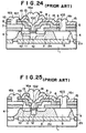
- Fig. 24 is a vertical cross sectional view showing a semiconductor device according to a first related art.
- the device includes p type silicon substrate 1, n + buried layer 2a, adjacent p + buried layer 2b, epitaxial silicon collector layer 3, silicon oxide 4 formed by LOCOS (local oxidation of silicon) and collector lead-out region 5.
- the device also includes silicon oxide 6, polysilicon base electrode 7, silicon oxide 8, outer base region 10, intrinsic base 11,second collector region 12, polysilicon emitter electrode 13 and single crystalline emitter region 14.
- the device further includes silicon oxide 15, aluminum alloy emitter electrode 16a, aluminum alloy base electrode 16b, aluminum alloy collector electrode 16c, first aperture 101, second aperture 102 and third aperture 103.
- a vertical bipolar transistor is fabricated with emitter 14, intrinsic base 11 and second collector 12, in the above semiconductor device, which are lead out through the electrodes isolated by silicon oxides 6, 8 and 15.
- Second collector 12 located directly beneath outer base 10 has a high collector concentration equal to that of the region directly beneath intrinsic base 11 in this semiconductor device. Whereas the high speed may be achieved to a certain extent, therefore, the collector-base capacitance intends to increase.
- Fig. 25 is a vertical cross sectional view showing another semiconductor device according to the first related art. Description for the same portions as those in Fig. 24 may be omitted in Fig. 25 with giving the same reference numerals. Note that a feature of collector 12 greatly differs from that in Fig. 24.
- the collector concentration directly beneath outer base 10 in the semiconductor device is controlled lower than that of the region directly beneath intrinsic base 11.
- low concentration collector region 3 is interposed between high concentration collector region 12 directly beneath intrinsic base 11 and n + buried layer 2a. Therefore, cut-off frequency f T may decrease even if the collector-base capacitance is small.
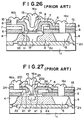
- Fig. 26 is a vertical cross sectional view showing a semiconductor device according to a second related art.
- the device includes p type silicon substrate 1, n + buried layer 2a, adjacent p+ buried layer 2b, epitaxial silicon collector layer 3, LOCOS silicon oxide 4 and collector lead-out region 5.
- the device also includes silicon oxide 6, polysilicon base electrode 7, silicon oxide 8, outer base 10, intrinsic base 11, second collector region 12, polysilicon emitter electrode 13 and single crystalline emitter region 14.
- the device further includes silicon oxide 15, aluminum alloy emitter electrode 16a, aluminum alloy base electrode 16b and aluminum alloy collector electrode 16c.
- a vertical bipolar transistor is fabricated with emitter 14, intrinsic base 11 and second collector 12, in the above semiconductor device, which are lead out through the electrodes isolated by silicon oxides 6, 8 and 15.
- single crystalline base 11 is epitaxially grown whole over Si collector region 12. Whereas there is no region called outer base 10, a portion directly beneath the emitter may be considered as the intrinsic base. Thus, the collector located direct beneath a peripheral base region of the intrinsic base may also have a high concentration.
- Fig. 27 is a vertical cross sectional view showing a semiconductor device according to a third related art.
- the device includes p-silicon substrate 1, n + buried layer 2a, adjacent p + buried layer 2b, epitaxial silicon collector layer 3, LOCOS silicon oxide 4 and collector lead-out region 5.
- the device also includes a silicon oxide 6, polysilicon base electrode 7, silicon oxide 8, intrinsic base 11, single crystalline Si intrinsic base layer 21, polycrystalline Si layer 22, single crystalline emitter region 24 and silicon oxide 25.
- the device further includes second collector region 12, polysilicon emitter electrode 13, silicon oxide 15, aluminum alloy emitter electrode 16a, aluminum alloy base electrode 16b and aluminum alloy collector electrode 16c.
- the device also includes aperture 201 for making silicon oxide 6 contact with single crystalline Si intrinsic base layer 21 and polycrystalline Si layer 22, and aperture 202 for making polysilicon emitter electrode 13 and single crystalline emitter region 23 contact with intrinsic base 21 and polycrystalline Si layer 41.
- aperture 202 must be formed by aligning with previously formed aperture 201 in the first and second related arts, the aperture may only be formed once according to the third related art, whereby miniaturization of the transistor may be achieved.
- An object of the present invention is to provide a semiconductor device capable of satisfying the contrary requests to achieve both the low collector concentration for reducing the parasitic capacitance and the high collector concentration for improving cut-off frequency f T simultaneously.
- the present invention is provided with a method for fabricating a semiconductor device comprising the steps of: forming a silicon material having a high concentration buried layer and a low concentration surface region; forming a single layer or multi-layered film on the surface of the silicon material; opening an aperture in the film by means of photolithography and dry etch; implanting phosphorous ions into the silicon material to form a first collector region adjacent to the buried layer before removing the photoresist; implanting boron ions into the surface of the silicon material to form an intrinsic base; implanting phosphorous ions selectively into the silicon material to form a second collector region between the intrinsic base and the first collector region with using the film used to form the aperture as the mask; and disposing a polysilicon emitter electrode for diffusing the dopant from the polysilicon emitter electrode into the intrinsic base region to form a single crystalline emitter region.
- the present invention is also provided with a method for fabricating a semiconductor device including a bipolar transistor having a base formed by epitaxial growth or ion implantation, wherein the bipolar transistor has an epitaxial silicon collector layer, a base region directly under an emitter defined as an intrinsic base and a peripheral region thereof defined as an outer base region, the method comprising the steps of: implanting ions into the collector layer to form a high concentration collector region at a location close to a buried region with using a photoresist used to form an aperture; forming the base region; and implanting ions into the collector layer to form a high concentration collector region directly beneath the base region.
- the present invention is further provided with a method for fabricating a semiconductor device comprising the steps of: forming a silicon material having a high concentration buried layer and a low concentration surface region; forming a first insulating film, a polysilicon base electrode and a photoresist on the silicon material; patterning the photoresist; opening an aperture in the polysilicon base electrode and the insulating film by anisotropic dry etching; implanting phosphorous ions to form a first collector region adjacent to the buried layer; growing a boron doped silicon by non-selective epitaxial growth; forming a single crystalline intrinsic base on the silicon material; forming a polycrystalline silicon on a region other than the intrinsic base; covering the surface with a second insulating film; patterning a photoresist and performing anisotropic dry etching to open an aperture on the intrinsic base; and implanting phosphorous ions to form a second collector region on the first collector region.
- the present invention is also provided with a method for fabricating a semiconductor device comprising the steps of: forming a silicon material having a high concentration buried layer and a low concentration surface region; forming a first insulating film on the silicon material; depositing a polysilicon base electrode; removing the undesired polysilicon by photolithography and anisotropic dry etching; covering the whole surface with a second insulating film having a different substance from that of the first insulating film; opening an aperture in the second insulating film and the polysilicon base electrode; implanting phosphorous ions to form a first collector region; forming a third insulating film having the same substance as that of the second insulating film; etching back the third insulating film by a thickness deposited just before to expose the first insulating film; etching the first insulating film in the lateral direction to expose the silicon material and a lower surface of the polysilicon base electrode; forming an intrinsic base and a polycrystalline outer base for connecting the intrinsic base with the
- the present invention is provided with a semiconductor device fabricated by any one of the methods described above.
- a base region on which an emitter is formed directly is referred to as an intrinsic base and a peripheral region thereof is called an outer base region.
- An effective thickness of a collector region in the bipolar transistor that is formed by an epitaxial growth, ion implantation and the like is defined as Wc which means a distance between the intrinsic base and buried layer 2a.
- a thickness of the intrinsic base is defined as WB.
- a total thickness originated from the junction interface between the outer base and the collector region through various films disposed thereon to a lower surface of the polysilicon emitter is defined as t.
- the t is expressed in Fig. 1 as a total thickness including the depth of outer base 10, the film thickness of polysilicon base electrode 7 and the film thickness of silicon oxide 8. This is a transistor structure defined by t ⁇ WB + Wc.
- the device may be produced by implanting ions into the epitaxial collector layer to form a high concentration collector region at a location close to a buried region with using a photoresist used to form an aperture, and then implanting ions into the collector layer to form a high concentration collector region directly beneath the base region after forming the base region.
- twice ion implantations may realize the improvement of cut-off frequency f T and the reduction of base-collector capacitance C CB at the same time.
- a boron-containing region may be formed at an interface between SiGe/Si collector in accordance with a pretreatment before SiGe/Si base growth.
- an addition of a dopant with an opposite conductivity for compensating the boron-containing region may be performed after forming the base to prevent an energy barrier from generating in the heterointerface.
- a semiconductor device and a method for manufacturing the device according to a first embodiment of the present invention will be described below with respect to the npn bipolar transistor, which may also be applied to the pnp bipolar transistor.
- Fig. 1 is a vertical cross sectional view showing the semiconductor device according to the first embodiment of the present invention.
- P type silicon substrate 1 has a crystal orientation of (100) and a resistivity of 10-20 ⁇ -cm.
- N + buried region 2a is separated from p + buried region 2b for the use of channel stop.
- N type epitaxial silicon collector layer 3 is formed over the surface of buried layers 2 and the surface of the silicon substrate in a region where no buried layer is present. Buried layers 2 may be slightly extended into the epitaxial growth layer due to the autodoping and diffusion of the dopant into the growth layer during the epitaxial growth. A region having a dopant concentration lower than 5 x 10 16 cm -3 may be determined as collector epitaxial silicon layer 3. An effective thickness of epitaxial silicon collector layer 3 may be defined as about 0.50 ⁇ m.
- LOCOS silicon oxide 4 is formed deeply sufficient to reach at p + buried layer 2b for isolating epitaxial silicon collector layer 3.
- a part of epitaxial silicon collector layer 3 is heavily doped to form n + collector lead-out region 5 that is connected with n + buried layer 2a.
- Silicone oxide 6 is formed over the surfaces of epitaxial silicon collector layer 3, LOCOS silicon oxide 4 and n + collector lead-out region 5.
- First aperture 101 for exposing a part of silicon collector layer 3 to form the base, and third aperture 103 for exposing collector lead-out region 5 are opened in silicon oxide 6.
- P + polysilicon base electrode 7 is formed selectively on silicon oxide 6.
- Polysilicon 7 contacts with silicon collector layer 3 within first aperture 101 and extends inwardly from an edge of first aperture 101.
- An edge of the extended portion of polysilicon base electrode 7 is referred to as second aperture 102.
- Polysilicon base electrode 7 is covered with silicon oxide 8.
- n type silicon first collector region 9 that is heavily doped relative to the original impurity concentration of epitaxial silicon collector layer 3.
- Outer base 10 is disposed between p + polysilicon base electrode 7 and epitaxial silicon collector layer 3.
- Intrinsic base 11 is disposed at an upper potion of epitaxial silicon collector layer 3 surrounded by outer base 10.
- n type silicon second collector region 12 that is heavily doped relative to the original impurity concentration of collector epitaxial silicon layer 3.
- N + polysilicon emitter electrode 13 is provided at a region directly on intrinsic base 11.
- N + single crystalline emitter region 14 is provided in intrinsic base region 11, which is formed by impurity diffusion from n + polysilicon emitter electrode 13.
- Silicon oxide 15 may cover these regions.
- Aluminum alloy emitter electrode 16a, aluminum alloy base electrode 16b and aluminum alloy collector electrode 16c contact with polysilicon emitter electrode 13, polysilicon base electrode 7 and collector lead-out region 5, respectively.
- a method for manufacturing the semiconductor device according to the first embodiment will be described with reference to the vertical cross sectional views in main process steps.
- Fig. 2A is a vertical cross sectional view just after forming polysilicon base electrode 7.
- P type silicon substrate 1 which has a crystal orientation of (100) and a resistivity of 20 ⁇ -cm is employed.
- N + buried layers 2a and p + buried region 2b are formed within the surface region of silicon substrate 1.
- a silicon oxide (not depicted in the figure) is formed over silicon substrate 1 by a known CDV or thermal oxidation.
- the silicon oxide has a thickness of several 100 nm (preferably from 300 nm to 700 nm, for example, 500 nm).
- a photoresist may be patterned on the silicon oxide by a normal lithography. The photoresist may be employed as a mask for removing selectively the silicon oxide at the surface by means of wet etching with a HF-based solution.
- Such a low acceleration energy is required for the ion implantation as to prevent the implanted ions from passing through the silicon oxide mask.
- the dopant was suitably implanted with an energy of 70 keV and at a dose of 5 x 10 15 cm -2 to realize a dopant concentration of about 1 x 10 19 cm -3 in the buried layer.
- Preferable implantation conditions are acceleration energy of 50-120 keV and dose of 5 x 10 15 to 2 x 10 16 cm -2 .
- n + buried layer 2a is formed.
- n - epitaxial silicon collector layer 3 After removing the silicon oxide completely, growing n - epitaxial silicon collector layer 3 by a usual process.
- a growth temperature is preferably 950-1050°C.
- SiH 4 or SiH 2 Cl 2 may be employed as a source gas and PH 3 as a dopant gas.
- the layer 3 may preferably has a thickness of 0.3-1.3 ⁇ m and may contain a dopant (phosphorous) of 5 x 10 15 to 5 x 10 16 cm -3 . In this case, a region that has a concentration less than 5 x 10 16 cm -3 is about 0.5 ⁇ m thick.
- n - epitaxial silicon collector layer 3 is grown on buried layers 2.
- LOCOS oxide 4 is formed for device isolation by growing a thermal oxide (not depicted in the figure) with a thickness of 20-50 nm over the surface of epitaxial layer 3 and further forming a silicon nitride (not depicted in the figure) with a thickness of 70-150 nm. Thereafter, patterning the photoresist (not depicted in the figure) by photolithography and removing the silicon oxide and nitride by dry etching subsequently.
- etching epitaxial silicon layer 3 to form a groove may suitably be about a half the thickness of the LOCOS oxide.
- a silicon oxide for isolation or LOCOS oxide 4 is formed in the device region by oxidization with protecting the region by the silicon nitride.
- LOCOS oxide 4 has a thickness of 300-1000 nm enough to reach at channel stop buried layer 2b. In this case, approximately 600 nm thickness was employed.
- the silicon nitride is removed with a heated phosphoric acid.
- N + collector lead-out region 5 is formed to reduce the collector resistance by doping phosphorous into the region by means of diffusion or ion implantation.
- silicon material 100 may be prepared.
- the surface of silicon material 100 is covered with silicon oxide 6 having a suitable thickness of 100-300 nm. In this case, 200 nm thickness is selected.
- First aperture 101 may be formed in silicon oxide 6 by known photolithography and etching to expose the surface of epitaxial silicon collector layer 3.
- polysilicon 7 with a thickness of 150-350 nm. In this case, 250 nm thickness is selected. Then, implanting boron ions into polysilicon 7 with such a low implantation energy as not to pass through polysilicon 7 at a dose capable of achieving a high dopant concentration of 1 x 10 20 cm -3 . In this case, 10 KeV and 1 x 10 16 cm -2 are employed.
- Fig. 2B is a vertical cross sectional view at the stage just after patterning photolithography 41 to form an aperture following the formation of silicon oxide 8 over polysilicon base electrode 7.
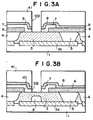
- first collector region 9 one of important process steps according to the present invention, that is, ion implantation of phosphorous is performed to form first collector region 9.
- the implantation was performed twice under conditions of 300 KeV, 1 x 10 13 cm -2 and 400 KeV, 2.5 x 10 13 cm -2 (Fig. 3B).
- silicon oxide 8 with a thickness of 50-300 nm by LPCVD (Fig. 4B). In this case, it was 200 nm.
- Outer base 10 that is formed with boron diffusion from polysilicon base electrode 7 may extend toward inside second aperture 102. Therefore, it is required that silicon oxide 8 formed on the side wall of polysilicon base electrode 7 has a thickness larger than the extension of outer base 10. In this case, it was about 300 nm.
- n + polysilicon emitter electrode 13 is formed. Then, performing heat treatment (at 1000 °C for 10 seconds, for example) for diffusing arsenic from polysilicon emitter electrode 13 into intrinsic base 11 to form n + single crystalline emitter region 14.
- 1.0 ⁇ m thick photoresist may intercept 99.99% phosphorous ions that are implanted with an acceleration energy of about 300 KeV.
- Implanting phosphorous ions into silicon with 300 KeV may cause the highest concentration in the phosphorous distribution at a depth of about 0.4 ⁇ m below the surface.
- the thickness of the collector region is insufficient, the capacitance may not be reduced even when the concentration of the collector region is sufficiently low. This is because the depletion layer between the base-collector may reach at n + buried layer 3 to prevent the depletion layer from extending additionally. Therefore, the thickness of epitaxial silicon collector layer 3 is required to be thicker to a certain extent.
- Phosphorous ions may be implanted into the region directly beneath the intrinsic base down to 0.61 ⁇ m if not into the region directly beneath the outer base even in the case where the depletion layer may extend the most in the above combination.
- the peak of the ion concentration may appear at a depth of 0.53 ⁇ m below the surface and thus the ions may reach at a position sufficiently close to the buried layer.
- About 2500 nm thick polysilicon, about 300 nm thick silicon oxide and about 1 ⁇ m thick photoresist are disposed on the outer base region during the ion implantation.
- phosphorous implanted at 400 KeV may be intercepted completely with only the photoresist and silicon oxide.
- a second embodiment of the present invention will be described with reference to the figures.
- the present embodiment differs in the intrinsic base formed by the non-selective epitaxial growth from the first embodiment.
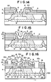
- Fig. 9 is a vertical cross sectional view showing a semiconductor device according to the second embodiment.
- Fig. 9 differs from Fig. 1 in that polysilicon base electrode 7 is present only on silicon oxide 6 and that epitaxial single crystalline Si intrinsic base layer 21 is disposed on epitaxial silicon collector layer 3 within aperture 104.
- Polycrystalline Si layer 22 may also be formed simultaneously when the base is epitaxially grown.
- the device shown in Fig. 9 includes p type silicon substrate 1, n + buried layer 2a, adjacent p + buried layer 2b, epitaxial silicon collector layer 3, LOCOS silicon oxide and collector lead-out region 5.
- the device also includes silicon oxide 6, polysilicon base electrode 7, silicon oxide 8, first collector region 9, outer base region 10, second collector region 12, polysilicon emitter electrode 13 and single crystalline emitter region 14.
- the device further includes silicon oxide 15, aluminum alloy emitter electrode 16a, aluminum alloy base electrode 16b and aluminum alloy collector electrode 16c.
- Fig. 10 shows the stage where silicon oxide 6 and polysilicon base electrode 7 are formed on silicon material 100 that is formed as the same manner as is in the first embodiment.
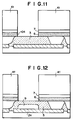
- Fig. 11 shows the stage where aperture 104 is opened in silicon oxide 6 and polysilicon base electrode 7 by patterning of photoresist 41 and anisotropic etching.
- Fig. 12 shows the stage where first collector region 9 is formed by implanting phosphorous ions consequently.
- boron-doped polysilicon by non-epitaxial growth as shown in Fig. 13A.
- SiGe may also be grown here, as is described later in the third embodiment.
- Single crystalline Si intrinsic base layer 21 is formed on epitaxial silicon collector layer 3 and polycrystalline silicon 22 on other region. Then, removing undesired portions of polysilicon base electrode 7 and polycrystalline silicon 22.
- the present embodiment may simplify the process because intrinsic base 21 is formed by the non-selective epitaxial growth.
- the device according to this embodiment may have a high-speed performance equal to that of the first embodiment.
- the present embodiment may also realize an extremely shallow base junction because the base region is formed by the epitaxial growth. Extremely high cut-off frequency f T may also be realized because of a short distance between the emitter, to where electrons are injected, and the collector at where the electrons may reach.
- the present embodiment employs the epitaxial growth that enables to grow materials other than Si, for example, a SiGe alloy, and to also fabricate the heterojunction bipolar transistor.
- the present embodiment is characterized in that the base consists of the SiGe alloy.
- Fig. 16 is a vertical cross sectional view showing a semiconductor device according to the third embodiment.
- P type silicon substrate 1 has a crystal orientation of (100) and a resistivity of 10-20 ⁇ -cm.
- Two buried layers 2a and 2b are formed within a surface region having a several ⁇ m depth inside silicon substrate 100.
- N + buried region 2a is separated from p + buried region 2b for the use of channel stop.
- N type epitaxial silicon collector layer 3 is formed over the surface of buried layers 2 and the surface of silicon substrate 100 in a region where no buried layer is present. Buried layers 2 may be slightly extended into the epitaxial growth layer due to the autodoping and diffusion of the dopant into the growth layer during the epitaxial growth.
- a region having a dopant concentration lower than 5 x 10 16 cm -3 may be defined as epitaxial silicon collector layer 3.
- An effective thickness of epitaxial silicon collector layer 3 may be defined about 0.50 ⁇ m as same as in the first embodiment.
- LOCOS silicon oxide 4 is formed deeply sufficient to reach at p + buried layer 2b for isolating epitaxial silicon collector layer 3.
- n + collector lead-out region 5 A part of n - epitaxial silicon layer 3 is heavily doped to form n + collector lead-out region 5 that is connected with n + buried layer 2a. Silicone oxide 6 is formed over the surfaces of epitaxial silicon collector layer 3, LOCOS silicon oxide 4 and n + collector lead-out region 5.
- First aperture 201 is formed in silicon oxide 6 for exposing a part of silicon collector layer 3 in order to form the base.
- P + polysilicon base electrode 7 is formed selectively on silicon oxide 6. Polysilicon 7 contacts with silicon collector layer 3 within first aperture 201 and extends inwardly from an edge of first aperture 201. Upper and side surfaces of polysilicon base electrode 7 are covered with silicon nitride 24, and a lower surface of a portion of polysilicon base electrode 7, that extends inwardly within aperture 201, contacts with p type polycrystalline layer 32.
- P type single crystalline intrinsic base layer 31 is epitaxially grown on epitaxial silicon collector layer 3 within aperture 201.
- n type silicon collector 9 that is heavily doped relative to the original impurity concentration of epitaxial silicon collector layer 3.
- n type silicon second collector region 12 that is heavily doped relative to the original impurity concentration of epitaxial silicon collector layer 3.
- Silicon oxide 41 is formed on silicon oxide 24 that covers polysilicon base electrode 7. An inner space within side walls of silicon oxide 41 is called aperture 202. N + polysilicon emitter electrode13 is disposed directly intrinsic base region 31 within aperture 202.
- N + single crystalline silicon emitter region 33 is formed on base region 31 by impurity diffusion from n + polysilicon emitter electrode 13.
- Silicon oxide 15 may cover these regions.
- Aluminum alloy emitter electrode 16a, base electrode 16b and collector electrode 16c contact with polysilicon emitter electrode 13, polysilicon base electrode 7 and collector lead-out region 5, respectively.
- a method for manufacturing the semiconductor device according to the third embodiment will be described with reference to the vertical cross sectional views in main process steps.
- Fig. 17A shows the stage just after forming silicon oxide 6 on silicon material 100 by the same process steps as in the first embodiment.
- Silicon oxide 6 has a thickness of about 100 nm within a preferable range of 50-200 nm.
- Fig. 17B is a vertical cross sectional view just after forming polysilicon base electrode 7 and silicon nitride 24.
- Non-doped polysilicon 7 may be deposited by the known LPCVD. A thickness thereof is preferably 200-400 nm, for example, about 300 nm in this case.
- Boron may be added to polysilicon 7 by ion implantation. Implantation conditions are, for example, acceleration energy of 10 keV and dose of 1 x 10 16 cm -2 . Then, removing undesired polysilicon 7 by photolithography and anisotropic dry etching. Thereafter, it is covered the whole surface with 150 nm thick silicon nitride 24.
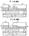
- Fig. 18A shows the stage where aperture 201 is opened in silicon nitride 24 and polysilicon base electrode 7 by patterning of photoresist 41 and anisotropic etching.
- Fig. 18B is across sectional view showing the stage where first collector region 9 is formed by implanting of phosphorous ions.
- Implantation conditions are preferably exemplified with acceleration energy of 300-500 KeV and dose of from 1 x 10 12 cm -2 to 5 x 10 13 cm -2 . In this case, the implantation was performed with acceleration energy of 300 KeV and dose of 5 x 10 13 cm - 2 .
- Fig 19A is a cross sectional view showing the stage where photoresist 41 is removed and silicon nitride 24 is deposited. After depositing silicon nitride 24, heating at 1000 °C for 2 hours in the nitrogen ambient for recovering the damages during the implantation and performing the activation of the implanted phosphorous.
- Fig 19B is a cross sectional view showing the stage where silicon nitride 24 is etched back by a thickness just before deposited by anisotropic dry etching to expose silicon oxide 6.
- Fig. 20A is a cross sectional view showing the stage where silicon oxide 6 is etched laterally with an HF-based solution to expose epitaxial silicon collector layer 3 and a lower surface of polysilicon base electrode 7.
- the size of laterally etched silicon oxide 6 for exposing polysilicon base electrode 7 is controlled at least larger than a thickness of intrinsic base 11 to be formed later.
- the side etch size may also be shorter than the thickness of the polysilicon base electrode.
- the lower surface of polysilicon base electrode 7 was exposed by about 150 nm.
- Fig. 20B is a cross sectional view showing the stage where intrinsic base 31 and polycrystalline layer 32 for making intrinsic base 31 contact with polysilicon base electrode 7 are formed by selective crystal growth.
- LPCVD and gas source MBE may be employed as growth conditions
- UHV/CVD is exemplified herein under a condition of a substrate temperature of 605 °C, Si 2 H 6 with a flow rate of 3 sccm and GeH 4 with a flow rate of 2 sccm.
- p type polycrystalline SiGe film 32 may be formed toward silicon collector layer 3 that includes the collector region from the lower surface of the extension of polysilicon base electrode 7.
- Base region 31 consisting of p type single crystalline SiGe alloy/single crystalline Si may be formed on the exposed portion of silicon collector layer 3.
- Polycrystalline SiGe alloy/polycrystalline Si multi-layered film 32 may contact with SiGe alloy/Si base region 31 as detailed below.
- the Ge concentration was about 10 %.
- a growth thickness is about 25 nm.
- the thickness may also be controlled thicker by a heat treatment in the following process within a range that does not cause any defect.
- the non-doped polycrystalline SiGe film may also be formed on the lower surface of the p + polysilicon simultaneously. Heating the polycrystalline film to add boron at a high concentration may realize a p + polycrystalline SiGe film.
- the intrinsic base layer consists of two layers: p + SiGe layer having a gradient Ge profile; and p type Si layer.
- the Ge profile, boron concentration profile and thickness thereof will be exemplified next.
- the layer which has a concentration profile of Ge in SiGe that decreases from 10 % to 0 % linearly, has a thickness of 40 nm.
- the 30 nm thick layer not containing Ge or consisting only of Si is present. Boron is added to both the layers at 5 x 10 18 cm -3 .
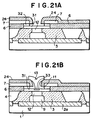
- Fig. 21A is a vertical cross sectional view showing the stage where second collector region 12 is formed by implanting phosphorous ions.
- the implantation condition of phosphorous is required to achieve a smooth connection with the phosphorous profile in first collector region 9.
- An example of the condition includes an acceleration energy of 200 KeV and a dose of 4 x 10 12 cm -2 .
- n + polysilicon emitter electrode 13 may be formed. Further, heating (at 930 °C for 10 seconds, for example) for diffusing phosphorous from polysilicon emitter electrode 13 into intrinsic base region 31 to form n + single crystalline emitter region 33.
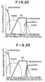
- Fig. 22 is a characteristic diagram showing an impurity profile in the SiGe base transistor according to the present invention, in which the transversal axis indicates depths ( ⁇ m) from the emitter interface of the poly/single crystalline emitter and the longitudinal axis impurity concentrations (cm -3 ) thereof.
- the emitter region with a depth of 30 nm from the surface, into which phosphorous is diffused from the polysilicon emitter.
- the region contains boron at about 5 x 10 18 cm -3 and Ge concentration increases monotonously from 0 % to 10 %.
- Phosphorous ions are implanted at a concentration higher than that of boron in the region into a portion near the surface of this region and also into another portion apart from the surface of the SiGe alloy layer (a portion that is 95 nm apart from the most surface).
- Fig. 23 shows an impurity profile in the art obtained from the SiGe base transistor formed by growing SiGe after implanting phosphorous ions previously.
- a difference from Fig. 22 lies in that the boron concentration is higher than the phosphorous concentration at a portion close to the heterointerface of SiGe/Si.
- the boron-doped region formed at the SiGe/Si interface can be completely compensated into n type with phosphorous.
- the present embodiment may miniaturize the device relative to the second embodiment because the base region (including the outer base) and the emitter region may be determined by photolithography once.
- the conventional method performs the implantation of phosphorous ions, the diffusion of phosphorous from the collector region and the cancellation of boron at the epiatxial SiGe/Si interface.
- a sufficiently high phosphorous concentration is required in the phosphorous diffusion to cancel boron.
- the present embodiment implants phosphorous ions with controlling the implantation energy in accordance with the interface depth and thus can reduce the phosphorous concentration as low as possible. Reduction of the collector concentration may decrease the base-collector junction capacitance and may further increase cut-off frequency f T .
- the semiconductor device according to the present invention has the following advantages compared to the semiconductor device in the art. First, improvement of cut-off frequency f T and reduction of collector-base capacitance C CB may be achieved at the same time.
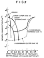
- Fig. 7 is an impurity profile in the transistor according to the present invention, in which the traversal axis indicates depths ( ⁇ m) from the emitter interface of the poly/single crystalline emitter and the longitudinal axis impurity concentrations (cm -3 ) thereof.
- the emitter consists of arsenic and has a depth of about 0.08 ⁇ m
- the base region consists of boron with a concentration of 10 18 cm -3 and has a depth of 0.08-0.15 ⁇ m
- the collector consists of phosphorous with a concentration of about 2 x 10 17 cm - 3 .
- the boron concentration that is 10 19 cm - 3 at the surface decreases to make a junction with phosphorous having a concentration of about 1 x 10 16 cm -3 at a depth of about 0.28 ⁇ m to where the outer base Extends.
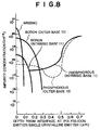
- Fig. 8 shows an impurity profile regarding the transistor in the art.
- the intrinsic region is similar to that in Fig. 7.
- the boron-doped outer base lies in a range from the surface to about 0.26 ⁇ m depth, and phosphorous with a concentration of 10 17 cm -3 is present beneath the outer base.
- the impurity concentration of the collector region directly beneath intrinsic base 11 is almost equal to that of the collector region adjacent to outer base 10.
- the impurity concentration of the intrinsic base 11 clearly differs from the impurity concentration of the region adjacent to outer base 11.
- the transistor according to the present invention the impurity concentration of the collector region directly beneath the intrinsic base is almost equal to that in the art, and the impurity concentration of the collector region adjacent to the outer base is equal to the original impurity concentration of epitaxial silicon collector layer 3.
- a capacitance per unit area of the outer base may not differ from that of the intrinsic base, and the both exhibit about 1.2 x 10 5 pF/cm 2 (Nc: 2 x 10 17 cm -3 ).
- the outer base capacitance per unit area is equal to that in the art.
- the outer base capacitance per unit area about 7 x 10 4 pF/cm 2 (Nc: 5 x 10 16 cm -3 ), is a half that in the art.
- the reduction of C CB and the increase of cut-off frequency f T can be achieved.
- the electric property variation due to the film thickness variation of the epitaxial silicon collector layer can be reduced by the process that may increase the concentration of the n - epitaxial silicon layer close to the n + buried layer.
- This effect may be obtained from the reason that ions can be implanted into a deep region only beneath the intrinsic base and thus the effective thickness variation of the epitaxial layer can be absorbed by the phosphorous ion implantation.
Landscapes
- Bipolar Transistors (AREA)
Applications Claiming Priority (2)
| Application Number | Priority Date | Filing Date | Title |
|---|---|---|---|
| JP09507598A JP3186691B2 (ja) | 1998-04-07 | 1998-04-07 | 半導体装置及びその形成方法 |
| JP9507598 | 1998-04-07 |
Publications (2)
| Publication Number | Publication Date |
|---|---|
| EP0949665A2 true EP0949665A2 (fr) | 1999-10-13 |
| EP0949665A3 EP0949665A3 (fr) | 2000-06-28 |
Family
ID=14127862
Family Applications (1)
| Application Number | Title | Priority Date | Filing Date |
|---|---|---|---|
| EP99106884A Withdrawn EP0949665A3 (fr) | 1998-04-07 | 1999-04-07 | Transistor bipolaire à haute vitesse et à faible capacité parasite ainsi que sa méthode de fabrication |
Country Status (5)
| Country | Link |
|---|---|
| US (1) | US6436781B2 (fr) |
| EP (1) | EP0949665A3 (fr) |
| JP (1) | JP3186691B2 (fr) |
| KR (1) | KR100294129B1 (fr) |
| CN (1) | CN1231506A (fr) |
Cited By (7)
| Publication number | Priority date | Publication date | Assignee | Title |
|---|---|---|---|---|
| EP1240671A1 (fr) * | 1999-11-26 | 2002-09-18 | Infineon Technologies AG | Sous-collecteur dope retrograde et son procede de production |
| WO2002097896A1 (fr) * | 2001-05-25 | 2002-12-05 | International Business Machines Corporation | Procede de fabrication d'un dispositif bipolaire npn haute tension a performances de courant alternatif ameliorees |
| DE10160509A1 (de) * | 2001-11-30 | 2003-06-12 | Ihp Gmbh | Halbleitervorrichtung und Verfahren zu ihrer Herstellung |
| DE10160511A1 (de) * | 2001-11-30 | 2003-06-12 | Ihp Gmbh | Bipolarer Transistor |
| WO2004049452A1 (fr) * | 2002-11-22 | 2004-06-10 | Austriamicrosystems Ag | Transistor pourvu d'une borne de base a faible impedance |
| DE10358046A1 (de) * | 2003-12-05 | 2005-07-07 | IHP GmbH - Innovations for High Performance Microelectronics/Institut für innovative Mikroelektronik | Bipolartransistor mit erhöhtem Basisanschlussgebiet und Verfahren zu seiner Herstellung |
| WO2018127514A1 (fr) | 2017-01-03 | 2018-07-12 | Technische Universiteit Delft | Dispositif à semiconducteur actif à capacité de jonction linéarisée |
Families Citing this family (36)
| Publication number | Priority date | Publication date | Assignee | Title |
|---|---|---|---|---|
| JP2001338930A (ja) * | 2000-05-29 | 2001-12-07 | Nec Corp | 半導体装置および半導体製造方法 |
| US6688335B2 (en) | 2000-07-14 | 2004-02-10 | Suzuki Sogyo Co., Ltd. | Liquid hammer prevention device |
| US6534372B1 (en) * | 2000-11-22 | 2003-03-18 | Newport Fab, Llc | Method for fabricating a self-aligned emitter in a bipolar transistor |
| JP2002206689A (ja) | 2000-11-24 | 2002-07-26 | Suzuki Sogyo Co Ltd | 配管直列型液撃防止器 |
| US6465870B2 (en) * | 2001-01-25 | 2002-10-15 | International Business Machines Corporation | ESD robust silicon germanium transistor with emitter NP-block mask extrinsic base ballasting resistor with doped facet region |
| US6770952B2 (en) * | 2001-04-30 | 2004-08-03 | Texas Instruments Incorporated | Integrated process for high voltage and high performance silicon-on-insulator bipolar devices |
| US6861324B2 (en) * | 2001-06-15 | 2005-03-01 | Maxim Integrated Products, Inc. | Method of forming a super self-aligned hetero-junction bipolar transistor |
| DE10134089A1 (de) * | 2001-07-13 | 2003-01-30 | Infineon Technologies Ag | Verfahren zur Herstellung eines Bipolartransistors mit Polysiliziumemitter |
| KR100437494B1 (ko) * | 2002-03-25 | 2004-06-25 | 주식회사 케이이씨 | 트랜지스터 및 그 제조 방법 |
| JP3761162B2 (ja) * | 2002-03-27 | 2006-03-29 | ローム株式会社 | バイポーラトランジスタ及びこれを用いた半導体装置 |
| US7521733B2 (en) * | 2002-05-14 | 2009-04-21 | Infineon Technologies Ag | Method for manufacturing an integrated circuit and integrated circuit with a bipolar transistor and a hetero bipolar transistor |
| US6869854B2 (en) * | 2002-07-18 | 2005-03-22 | International Business Machines Corporation | Diffused extrinsic base and method for fabrication |
| US6911716B2 (en) * | 2002-09-09 | 2005-06-28 | Lucent Technologies, Inc. | Bipolar transistors with vertical structures |
| JP2004111852A (ja) | 2002-09-20 | 2004-04-08 | Fujitsu Ltd | 半導体装置及びその製造方法 |
| DE10306597B4 (de) * | 2003-02-17 | 2005-11-17 | Infineon Technologies Ag | Verfahren zum Herstellen einer Halbleiterstruktur mit erhöhter Durchbruchspannung durch tieferliegenden Subkollektorabschnitt |
| US7541624B2 (en) * | 2003-07-21 | 2009-06-02 | Alcatel-Lucent Usa Inc. | Flat profile structures for bipolar transistors |
| US7084485B2 (en) * | 2003-12-31 | 2006-08-01 | Freescale Semiconductor, Inc. | Method of manufacturing a semiconductor component, and semiconductor component formed thereby |
| US7075126B2 (en) * | 2004-02-27 | 2006-07-11 | International Business Machines Corporation | Transistor structure with minimized parasitics and method of fabricating the same |
| US20060170074A1 (en) * | 2004-12-28 | 2006-08-03 | Yoshikazu Ibara | Semiconductor device |
| JP2006210790A (ja) * | 2005-01-31 | 2006-08-10 | Renesas Technology Corp | 半導体装置およびその製造方法 |
| US20080217742A1 (en) * | 2007-03-09 | 2008-09-11 | International Business Machines Corporation | Tailored bipolar transistor doping profile for improved reliability |
| US7750371B2 (en) * | 2007-04-30 | 2010-07-06 | International Business Machines Corporation | Silicon germanium heterojunction bipolar transistor structure and method |
| KR101126933B1 (ko) * | 2008-09-02 | 2012-03-20 | 주식회사 동부하이텍 | 폴리에미터형 바이폴라 트랜지스터, bcd 소자, 폴리에미터형 바이폴라 트랜지스터의 제조 방법 및 bcd 소자의 제조 방법 |
| CN101714553B (zh) * | 2008-09-29 | 2011-05-11 | 凹凸电子(武汉)有限公司 | 单元晶体管、集成电路及显示系统 |
| CN101728263B (zh) * | 2008-10-24 | 2011-07-06 | 中芯国际集成电路制造(上海)有限公司 | 控制源/漏结电容的方法和pmos晶体管的形成方法 |
| US8735289B2 (en) * | 2010-11-29 | 2014-05-27 | Infineon Technologies Ag | Method of contacting a doping region in a semiconductor substrate |
| CN102543725A (zh) * | 2010-12-20 | 2012-07-04 | 上海华虹Nec电子有限公司 | 高速锗硅异质结双极晶体管的制造方法 |
| CN102543726B (zh) * | 2010-12-20 | 2015-02-04 | 上海华虹宏力半导体制造有限公司 | 高压锗硅异质结双极晶体管的制造方法 |
| CN103137675B (zh) * | 2011-11-23 | 2016-04-13 | 上海华虹宏力半导体制造有限公司 | 具有高击穿电压的锗硅异质结双极晶体管结构及其制作方法 |
| CN102651384B (zh) * | 2012-05-16 | 2014-09-17 | 清华大学 | 嵌入式外延外基区双极晶体管及其制备方法 |
| CN103000679B (zh) * | 2012-12-20 | 2015-05-06 | 清华大学 | 低电阻多晶连接基区全自对准双极晶体管及其制备方法 |
| CN103022110B (zh) * | 2012-12-20 | 2015-07-29 | 清华大学 | 金属硅化物抬升外基区全自对准双极晶体管及其制备方法 |
| US11563084B2 (en) | 2019-10-01 | 2023-01-24 | Analog Devices International Unlimited Company | Bipolar junction transistor, and a method of forming an emitter for a bipolar junction transistor |
| US11404540B2 (en) | 2019-10-01 | 2022-08-02 | Analog Devices International Unlimited Company | Bipolar junction transistor, and a method of forming a collector for a bipolar junction transistor |
| US11355585B2 (en) | 2019-10-01 | 2022-06-07 | Analog Devices International Unlimited Company | Bipolar junction transistor, and a method of forming a charge control structure for a bipolar junction transistor |
| CN111739939B (zh) * | 2020-07-06 | 2024-12-06 | 重庆邮电大学 | 一种高频硅锗异质结双极晶体管及其制造方法 |
Family Cites Families (11)
| Publication number | Priority date | Publication date | Assignee | Title |
|---|---|---|---|---|
| JPH021934A (ja) | 1988-06-10 | 1990-01-08 | Fujitsu Ltd | バイポーラ半導体装置の製造方法 |
| JPH03138946A (ja) * | 1989-10-24 | 1991-06-13 | Sony Corp | 半導体装置 |
| JP3254691B2 (ja) | 1990-08-31 | 2002-02-12 | 日本電気株式会社 | バイポーラトランジスタの製造方法 |
| JPH06216145A (ja) | 1992-01-28 | 1994-08-05 | Fujitsu Ltd | 半導体装置の製造方法 |
| JPH05267317A (ja) | 1992-03-18 | 1993-10-15 | Fujitsu Ltd | 半導体装置及びその製造方法 |
| JP2842042B2 (ja) | 1992-05-08 | 1998-12-24 | 日本電気株式会社 | 半導体装置 |
| JP2551364B2 (ja) * | 1993-11-26 | 1996-11-06 | 日本電気株式会社 | 半導体装置 |
| JP2606141B2 (ja) * | 1994-06-16 | 1997-04-30 | 日本電気株式会社 | 半導体装置およびその製造方法 |
| JP2748898B2 (ja) * | 1995-08-31 | 1998-05-13 | 日本電気株式会社 | 半導体装置およびその製造方法 |
| JP3562284B2 (ja) | 1998-01-13 | 2004-09-08 | 株式会社日立製作所 | バイポーラトランジスタおよびその製造方法 |
| JP3257523B2 (ja) * | 1998-10-07 | 2002-02-18 | 日本電気株式会社 | 半導体装置の製造方法 |
-
1998
- 1998-04-07 JP JP09507598A patent/JP3186691B2/ja not_active Expired - Lifetime
-
1999
- 1999-04-06 CN CN99105440A patent/CN1231506A/zh active Pending
- 1999-04-06 KR KR1019990011870A patent/KR100294129B1/ko not_active Expired - Fee Related
- 1999-04-07 EP EP99106884A patent/EP0949665A3/fr not_active Withdrawn
-
2001
- 2001-02-26 US US09/791,800 patent/US6436781B2/en not_active Expired - Lifetime
Cited By (13)
| Publication number | Priority date | Publication date | Assignee | Title |
|---|---|---|---|---|
| US6806152B1 (en) | 1999-11-26 | 2004-10-19 | Infineon Technologies Ag | Retrograde doped buried layer transistor and method for producing the same |
| EP1240671A1 (fr) * | 1999-11-26 | 2002-09-18 | Infineon Technologies AG | Sous-collecteur dope retrograde et son procede de production |
| WO2002097896A1 (fr) * | 2001-05-25 | 2002-12-05 | International Business Machines Corporation | Procede de fabrication d'un dispositif bipolaire npn haute tension a performances de courant alternatif ameliorees |
| CN1303696C (zh) * | 2001-05-25 | 2007-03-07 | 国际商业机器公司 | Ac性能改进的高电压npn双极型器件的生产方法 |
| US7323390B2 (en) | 2001-11-30 | 2008-01-29 | Ihp Gmbh - Innovations For High Performance Microelectronics/Institut Fur Innovative Mikroelektronik | Semiconductor device and method for production thereof |
| DE10160509A1 (de) * | 2001-11-30 | 2003-06-12 | Ihp Gmbh | Halbleitervorrichtung und Verfahren zu ihrer Herstellung |
| DE10160511A1 (de) * | 2001-11-30 | 2003-06-12 | Ihp Gmbh | Bipolarer Transistor |
| WO2004049452A1 (fr) * | 2002-11-22 | 2004-06-10 | Austriamicrosystems Ag | Transistor pourvu d'une borne de base a faible impedance |
| DE10358046A1 (de) * | 2003-12-05 | 2005-07-07 | IHP GmbH - Innovations for High Performance Microelectronics/Institut für innovative Mikroelektronik | Bipolartransistor mit erhöhtem Basisanschlussgebiet und Verfahren zu seiner Herstellung |
| DE10358046B4 (de) * | 2003-12-05 | 2010-06-17 | Ihp Gmbh - Innovations For High Performance Microelectronics / Leibniz-Institut Für Innovative Mikroelektronik | Bipolartransistor mit erhöhtem Basisanschlussgebiet und Verfahren zu seiner Herstellung |
| US7777255B2 (en) | 2003-12-05 | 2010-08-17 | IHP GmbH—Innovations for High Performance Microelectronics / Leibniz-Instut für innovative Mikroelektronik | Bipolar transistor with raised base connection region and process for the production thereof |
| WO2018127514A1 (fr) | 2017-01-03 | 2018-07-12 | Technische Universiteit Delft | Dispositif à semiconducteur actif à capacité de jonction linéarisée |
| NL2018115B1 (en) * | 2017-01-03 | 2018-07-25 | Univ Delft Tech | Active semiconductor device with linearized depletion capacitance |
Also Published As
| Publication number | Publication date |
|---|---|
| US20010009793A1 (en) | 2001-07-26 |
| JPH11297708A (ja) | 1999-10-29 |
| KR19990082963A (ko) | 1999-11-25 |
| CN1231506A (zh) | 1999-10-13 |
| EP0949665A3 (fr) | 2000-06-28 |
| JP3186691B2 (ja) | 2001-07-11 |
| KR100294129B1 (ko) | 2001-06-15 |
| US6436781B2 (en) | 2002-08-20 |
Similar Documents
| Publication | Publication Date | Title |
|---|---|---|
| US6436781B2 (en) | High speed and low parasitic capacitance semiconductor device and method for fabricating the same | |
| US9508824B2 (en) | Method for fabricating a bipolar transistor having self-aligned emitter contact | |
| EP1710842B1 (fr) | Méthode de fabrication d'un dispositif semi-conducteur du type transistor bipolaire et MISFET | |
| US5399511A (en) | Method of manufacturing a hetero bipolar transistor | |
| KR100244812B1 (ko) | 반도체 장치 및 그 제조 방법 | |
| EP0701287B1 (fr) | Transistor bipolaire sans fuite de courant à travers la région de base mince et procédé de fabrication | |
| JP3329640B2 (ja) | 半導体装置の製造方法 | |
| US6913981B2 (en) | Method of fabricating a bipolar transistor using selective epitaxially grown SiGe base layer | |
| US5420053A (en) | Method for manufacturing semiconductor device having bipolar transistor and polycrystalline silicon resistor | |
| JP2002525874A (ja) | バイポーラトランジスタ及びその製造方法 | |
| US20030107051A1 (en) | Super self -aligned heterojunction biplar transistor and its manufacturing method | |
| JPH10112507A (ja) | 半導体装置の製造方法 | |
| CN209471966U (zh) | 集成电路 | |
| US6744080B2 (en) | Method of manufacturing a bipolar transistor of double-polysilicon, heterojunction-base type and corresponding transistor | |
| WO1984004853A1 (fr) | Procede de fabrication d'un dispositif a semi-conducteur | |
| US7511317B2 (en) | Porous silicon for isolation region formation and related structure | |
| US6806159B2 (en) | Method for manufacturing a semiconductor device with sinker contact region | |
| JP3142336B2 (ja) | 半導体装置及びその製造方法 | |
| JP3456864B2 (ja) | 半導体装置及びその製造方法 | |
| JP2680358B2 (ja) | 半導体素子の製造方法 | |
| JP3254691B2 (ja) | バイポーラトランジスタの製造方法 | |
| JP3332079B2 (ja) | 半導体装置及びその製造方法 | |
| JP3908023B2 (ja) | 半導体装置の製造方法 | |
| US7794540B2 (en) | Method of manufacturing a semiconductor device | |
| US7064042B1 (en) | Self aligned compact bipolar junction transistor layout, and method of making same |
Legal Events
| Date | Code | Title | Description |
|---|---|---|---|
| PUAI | Public reference made under article 153(3) epc to a published international application that has entered the european phase |
Free format text: ORIGINAL CODE: 0009012 |
|
| AK | Designated contracting states |
Kind code of ref document: A2 Designated state(s): DE GB NL |
|
| AX | Request for extension of the european patent |
Free format text: AL;LT;LV;MK;RO;SI |
|
| PUAL | Search report despatched |
Free format text: ORIGINAL CODE: 0009013 |
|
| AK | Designated contracting states |
Kind code of ref document: A3 Designated state(s): AT BE CH CY DE DK ES FI FR GB GR IE IT LI LU MC NL PT SE |
|
| AX | Request for extension of the european patent |
Free format text: AL;LT;LV;MK;RO;SI |
|
| 17P | Request for examination filed |
Effective date: 20000524 |
|
| AKX | Designation fees paid |
Free format text: DE GB NL |
|
| RAP1 | Party data changed (applicant data changed or rights of an application transferred) |
Owner name: NEC ELECTRONICS CORPORATION |
|
| 17Q | First examination report despatched |
Effective date: 20060904 |
|
| STAA | Information on the status of an ep patent application or granted ep patent |
Free format text: STATUS: THE APPLICATION HAS BEEN WITHDRAWN |
|
| 18W | Application withdrawn |
Effective date: 20070118 |