EP0949667A1 - Cellule mémoire électriquement programmable - Google Patents
Cellule mémoire électriquement programmable Download PDFInfo
- Publication number
- EP0949667A1 EP0949667A1 EP99410021A EP99410021A EP0949667A1 EP 0949667 A1 EP0949667 A1 EP 0949667A1 EP 99410021 A EP99410021 A EP 99410021A EP 99410021 A EP99410021 A EP 99410021A EP 0949667 A1 EP0949667 A1 EP 0949667A1
- Authority
- EP
- European Patent Office
- Prior art keywords
- grid
- control grid
- layer
- memory cell
- conductive
- Prior art date
- Legal status (The legal status is an assumption and is not a legal conclusion. Google has not performed a legal analysis and makes no representation as to the accuracy of the status listed.)
- Withdrawn
Links
- 125000006850 spacer group Chemical group 0.000 claims abstract description 16
- 239000004020 conductor Substances 0.000 claims abstract description 14
- 238000000034 method Methods 0.000 claims abstract description 12
- 239000011810 insulating material Substances 0.000 claims abstract description 10
- 238000004519 manufacturing process Methods 0.000 claims abstract description 8
- 239000000463 material Substances 0.000 claims abstract description 6
- 238000005530 etching Methods 0.000 claims abstract description 3
- 238000000151 deposition Methods 0.000 claims abstract 2
- 229910021420 polycrystalline silicon Inorganic materials 0.000 claims description 7
- 229910052581 Si3N4 Inorganic materials 0.000 claims description 3
- HQVNEWCFYHHQES-UHFFFAOYSA-N silicon nitride Chemical compound N12[Si]34N5[Si]62N3[Si]51N64 HQVNEWCFYHHQES-UHFFFAOYSA-N 0.000 claims description 3
- 230000001590 oxidative effect Effects 0.000 claims description 2
- 239000000758 substrate Substances 0.000 description 5
- VYPSYNLAJGMNEJ-UHFFFAOYSA-N Silicium dioxide Chemical compound O=[Si]=O VYPSYNLAJGMNEJ-UHFFFAOYSA-N 0.000 description 4
- 229910052814 silicon oxide Inorganic materials 0.000 description 4
- 238000009413 insulation Methods 0.000 description 3
- XUIMIQQOPSSXEZ-UHFFFAOYSA-N Silicon Chemical compound [Si] XUIMIQQOPSSXEZ-UHFFFAOYSA-N 0.000 description 2
- 238000005516 engineering process Methods 0.000 description 2
- 229910052751 metal Inorganic materials 0.000 description 2
- 239000002184 metal Substances 0.000 description 2
- 229910021421 monocrystalline silicon Inorganic materials 0.000 description 2
- 230000003647 oxidation Effects 0.000 description 2
- 238000007254 oxidation reaction Methods 0.000 description 2
- 229910052710 silicon Inorganic materials 0.000 description 2
- 239000010703 silicon Substances 0.000 description 2
- 229910052782 aluminium Inorganic materials 0.000 description 1
- XAGFODPZIPBFFR-UHFFFAOYSA-N aluminium Chemical compound [Al] XAGFODPZIPBFFR-UHFFFAOYSA-N 0.000 description 1
- 230000015572 biosynthetic process Effects 0.000 description 1
- 230000000694 effects Effects 0.000 description 1
- 230000008030 elimination Effects 0.000 description 1
- 238000003379 elimination reaction Methods 0.000 description 1
- 230000006870 function Effects 0.000 description 1
- 238000002513 implantation Methods 0.000 description 1
- 238000011065 in-situ storage Methods 0.000 description 1
- 239000012212 insulator Substances 0.000 description 1
- 238000002955 isolation Methods 0.000 description 1
- 238000001465 metallisation Methods 0.000 description 1
- 238000012986 modification Methods 0.000 description 1
- 230000004048 modification Effects 0.000 description 1
- 150000004767 nitrides Chemical class 0.000 description 1
- 239000004065 semiconductor Substances 0.000 description 1
Images
Classifications
-
- H—ELECTRICITY
- H10—SEMICONDUCTOR DEVICES; ELECTRIC SOLID-STATE DEVICES NOT OTHERWISE PROVIDED FOR
- H10D—INORGANIC ELECTRIC SEMICONDUCTOR DEVICES
- H10D30/00—Field-effect transistors [FET]
- H10D30/01—Manufacture or treatment
- H10D30/021—Manufacture or treatment of FETs having insulated gates [IGFET]
- H10D30/0411—Manufacture or treatment of FETs having insulated gates [IGFET] of FETs having floating gates
-
- H—ELECTRICITY
- H10—SEMICONDUCTOR DEVICES; ELECTRIC SOLID-STATE DEVICES NOT OTHERWISE PROVIDED FOR
- H10D—INORGANIC ELECTRIC SEMICONDUCTOR DEVICES
- H10D30/00—Field-effect transistors [FET]
- H10D30/60—Insulated-gate field-effect transistors [IGFET]
- H10D30/68—Floating-gate IGFETs
- H10D30/6891—Floating-gate IGFETs characterised by the shapes, relative sizes or dispositions of the floating gate electrode
- H10D30/6893—Floating-gate IGFETs characterised by the shapes, relative sizes or dispositions of the floating gate electrode wherein the floating gate has multiple non-connected parts, e.g. multi-particle floating gate
Definitions
- the present invention relates to the field of cells memory achievable in MOS technology.
- the present invention relates to a memory cell comprising a control grid and a floating grid in which the floating grid is arranged laterally with respect to the control grid.
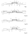
- FIG. 1 represents a memory cell of the type described in the aforementioned patent.
- the cell is formed in a monocrystalline silicon substrate 1, more particularly in an active area of this substrate delimited by a thick oxide layer 2.
- the upper surface of the semiconductor substrate is coated with a thin layer of silicon oxide 3 on which a polycrystalline silicon control grid is formed 4.
- the side walls of the polycrystalline silicon grid are insulated by a layer of silicon oxide 5 and polycrystalline silicon spacers 7 and 8 are formed on either side of the grid.
- the lateral conductive spacers 7 and 8 are formed above respective areas of source and drain extension 9 and 10.
- the substrate is of type P
- the source and drain extensions are of type N.
- the cell comprises source and drain zones 11 and 12 of type N + which are more heavily doped.
- the cell illustrated in FIG. 1 is not not completed. To complete it, it remains to establish contacts with the source, drain and control gate regions.
- the cell includes a single lateral spacer 8 above a drain extension.
- the present invention aims to provide a cell electrically programmable memory in which the grid floating is lateral to the control grid and which is particularly simple to manufacture by compatible processes with methods of manufacturing CMOS structures.
- the present invention provides for a method of manufacturing an electric memory cell programmable with lateral floating grid in relation to the control grid, comprising the steps of forming an isolated control grid on an active area; form a thin insulating layer around the control grid; deposit successively a thin layer of a conductive material and a layer of insulating material; anisotropically etch the insulating material for forming spacers of this material; and remove the uncoated parts of the conductive thin layer spacers.
- the conductive material is doped polycrystalline silicon.
- the conductive material has a thickness of 5 to 20 nm.
- the insulating material is silicon nitride.
- the method further comprises the step of oxidizing the visible parts of the conductive regions.
- the present invention also relates to a cell memory with control grid and lateral floating grid, comprising on the side walls of the control grid insulating spacers under which a thin layer is arranged of a conductive material.
- the cell is formed in a active area of a monocrystalline silicon substrate 1 delimited by a thick oxide region 2.
- This thick oxide region can be formed by any means and other methods of isolating a active zone can be used.
- a grid insulated conductor 4 on a gate insulation layer 3, commonly a layer of silicon oxide. Possibly, immediately after the grid is formed, regions are formed source and drain lightly doped using the grid and thick oxide as a mask. Note that, according to a variant, we can omit this step of forming regions of lightly doped source and drain.
- a thin layer of a conductive material 21 is formed on the oxide layer 3 .
- This thin layer may for example have a thickness of on the order of only 5 to 20 nm, for example 10 nm.
- the material conductor can be polycrystalline silicon, doped in situ or doped by subsequent implantation, or a metal.
- a layer of thick insulation preferably nitride silicon 22.
- the step of the Figure 2C is followed by an oxidation step to oxidize and insulate the apparent surfaces of the shaped regions L 25 and 26 constituting a floating grid.
- the conductive material from which layer 21 is formed is a material oxidizable such as polycrystalline silicon or a metal suitably chosen, for example aluminum. This isolation by oxidation avoids any short circuit with metallizations formed later.
- FIG. 2C the formation of drain and source zones 28 and 29. Then, in a conventional manner, drain contacts, source and control grid.
- the present invention is capable of various variants and modifications which will appear to the man of art.
- the floating grids are not necessarily arranged above source and drain extension regions.
- the insulation placed under the floating grilles will, depending on the type of memory that one wishes to achieve, of a thickness proper to operate by tunnel effect or not. We could also provide a symmetrical or asymmetrical structure like this has was disclosed in the aforementioned patent.
- the insulating material placed under the floating grid has been described previously as being a silicon oxide, other materials insulators or combinations of insulating materials may be used.
Landscapes
- Non-Volatile Memory (AREA)
- Semiconductor Memories (AREA)
Abstract
Description
Claims (6)
- Procédé de fabrication d'une cellule mémoire électriquement programmable à grille flottante latérale par rapport à la grille de commande, caractérisé en ce qu'il comprend les étapes suivantes :former une grille de commande isolée (4) sur une zone active ;former une couche mince isolante (5) autour de la grille de commande ;déposer successivement une couche mince d'un matériau conducteur (21) et une couche d'un matériau isolant (22) ;graver de façon anisotrope le matériau isolant pour former des espaceurs (23, 24) de ce matériau ; etéliminer les parties de la couche mince conductrice (21) non revêtues des espaceurs.
- Procédé selon la revendication 1, caractérisé en ce que le matériau conducteur est du silicium polycristallin dopé.
- Procédé selon la revendication 1 ou 2, caractérisé en ce que le matériau conducteur a une épaisseur de 5 à 20 nm.
- Procédé selon la revendication 1, caractérisé en ce que le matériau isolant est du nitrure de silicium.
- Procédé selon la revendication 1, caractérisé en ce qu'il comprend en outre l'étape consistant à oxyder les parties apparentes des régions conductrices.
- Cellule mémoire à grille de commande et grille flottante latérale, caractérisée en ce qu'elle comprend sur les parois latérales de la grille de commande des espaceurs isolants (23, 24) sous lesquels est disposée une couche mince (25, 26) d'un matériau conducteur.
Applications Claiming Priority (2)
| Application Number | Priority Date | Filing Date | Title |
|---|---|---|---|
| FR9804005 | 1998-03-26 | ||
| FR9804005A FR2776830B1 (fr) | 1998-03-26 | 1998-03-26 | Cellule memoire electriquement programmable |
Publications (1)
| Publication Number | Publication Date |
|---|---|
| EP0949667A1 true EP0949667A1 (fr) | 1999-10-13 |
Family
ID=9524714
Family Applications (1)
| Application Number | Title | Priority Date | Filing Date |
|---|---|---|---|
| EP99410021A Withdrawn EP0949667A1 (fr) | 1998-03-26 | 1999-03-26 | Cellule mémoire électriquement programmable |
Country Status (3)
| Country | Link |
|---|---|
| US (2) | US6297093B1 (fr) |
| EP (1) | EP0949667A1 (fr) |
| FR (1) | FR2776830B1 (fr) |
Families Citing this family (8)
| Publication number | Priority date | Publication date | Assignee | Title |
|---|---|---|---|---|
| JP4030193B2 (ja) * | 1998-07-16 | 2008-01-09 | 株式会社半導体エネルギー研究所 | 半導体装置の作製方法 |
| US6703298B2 (en) * | 2002-05-23 | 2004-03-09 | Tower Semiconductor Ltd. | Self-aligned process for fabricating memory cells with two isolated floating gates |
| JP4683817B2 (ja) * | 2002-09-27 | 2011-05-18 | 株式会社半導体エネルギー研究所 | 半導体装置の作製方法 |
| JP4454921B2 (ja) * | 2002-09-27 | 2010-04-21 | 株式会社半導体エネルギー研究所 | 半導体装置の作製方法 |
| US7265917B2 (en) | 2003-12-23 | 2007-09-04 | Carl Zeiss Smt Ag | Replacement apparatus for an optical element |
| JP4521597B2 (ja) * | 2004-02-10 | 2010-08-11 | ルネサスエレクトロニクス株式会社 | 半導体記憶装置およびその製造方法 |
| KR100650369B1 (ko) * | 2004-10-01 | 2006-11-27 | 주식회사 하이닉스반도체 | 폴리실리콘부유측벽을 갖는 비휘발성메모리장치 및 그제조 방법 |
| US7773416B2 (en) * | 2006-05-26 | 2010-08-10 | Macronix International Co., Ltd. | Single poly, multi-bit non-volatile memory device and methods for operating the same |
Citations (3)
| Publication number | Priority date | Publication date | Assignee | Title |
|---|---|---|---|---|
| US4620361A (en) * | 1984-05-17 | 1986-11-04 | Kabushiki Kaisha Toshiba | Method for producing a semiconductor device with a floating gate |
| GB2311167A (en) * | 1996-03-11 | 1997-09-17 | Hyundai Electronics Ind | Flash EEPROM cell |
| US5707897A (en) * | 1996-05-16 | 1998-01-13 | Taiwan Semiconductor Manufacturing Company Ltd. | Non-volatile-memory cell for electrically programmable read only memory having a trench-like coupling capacitors |
Family Cites Families (7)
| Publication number | Priority date | Publication date | Assignee | Title |
|---|---|---|---|---|
| JPH04151852A (ja) * | 1990-10-15 | 1992-05-25 | Mitsubishi Electric Corp | 半導体装置の製造方法 |
| US5338952A (en) * | 1991-06-07 | 1994-08-16 | Sharp Kabushiki Kaisha | Non-volatile memory |
| FR2718289B1 (fr) | 1994-03-30 | 1996-08-02 | Sgs Thomson Microelectronics | Cellule mémoire électriquement programmable. |
| US5429969A (en) * | 1994-05-31 | 1995-07-04 | Motorola, Inc. | Process for forming electrically programmable read-only memory cell with a merged select/control gate |
| US5760435A (en) * | 1996-04-22 | 1998-06-02 | Chartered Semiconductor Manufacturing, Ltd. | Use of spacers as floating gates in EEPROM with doubled storage efficiency |
| US5759920A (en) * | 1996-11-15 | 1998-06-02 | International Business Machines Corporation | Process for making doped polysilicon layers on sidewalls |
| US5969383A (en) * | 1997-06-16 | 1999-10-19 | Motorola, Inc. | Split-gate memory device and method for accessing the same |
-
1998
- 1998-03-26 FR FR9804005A patent/FR2776830B1/fr not_active Expired - Fee Related
-
1999
- 1999-03-25 US US09/276,003 patent/US6297093B1/en not_active Expired - Lifetime
- 1999-03-26 EP EP99410021A patent/EP0949667A1/fr not_active Withdrawn
-
2001
- 2001-08-10 US US09/928,147 patent/US6521942B2/en not_active Expired - Lifetime
Patent Citations (3)
| Publication number | Priority date | Publication date | Assignee | Title |
|---|---|---|---|---|
| US4620361A (en) * | 1984-05-17 | 1986-11-04 | Kabushiki Kaisha Toshiba | Method for producing a semiconductor device with a floating gate |
| GB2311167A (en) * | 1996-03-11 | 1997-09-17 | Hyundai Electronics Ind | Flash EEPROM cell |
| US5707897A (en) * | 1996-05-16 | 1998-01-13 | Taiwan Semiconductor Manufacturing Company Ltd. | Non-volatile-memory cell for electrically programmable read only memory having a trench-like coupling capacitors |
Also Published As
| Publication number | Publication date |
|---|---|
| FR2776830B1 (fr) | 2001-11-23 |
| US6521942B2 (en) | 2003-02-18 |
| US20020001903A1 (en) | 2002-01-03 |
| FR2776830A1 (fr) | 1999-10-01 |
| US6297093B1 (en) | 2001-10-02 |
Similar Documents
| Publication | Publication Date | Title |
|---|---|---|
| EP0258141B1 (fr) | Circuit intégré MIS tel qu'une cellule de mémoire EPROM et son procédé de fabrication | |
| EP0426250B1 (fr) | Procédé pour fabriquer un dispositif à transistors MIS ayant une grille débordant sur les portions des régions de source et de drain faiblement dopées | |
| FR2795555A1 (fr) | Procede de fabrication d'un dispositif semi-conducteur comprenant un empilement forme alternativement de couches de silicium et de couches de materiau dielectrique | |
| EP0426251A1 (fr) | Procédé pour fabriquer un dispositif à transistors MIS ayant une électrode de grille en forme de "T" inversé | |
| FR2795554A1 (fr) | Procede de gravure laterale par trous pour fabriquer des dis positifs semi-conducteurs | |
| FR2823009A1 (fr) | Procede de fabrication d'un transistor vertical a grille isolee a faible recouvrement de la grille sur la source et sur le drain, et circuit integre comportant un tel transistor | |
| EP1292974A1 (fr) | Procede de realisation d'un composant electronique a source, drain et grille auto-alignes, en architecture damascene. | |
| FR2728388A1 (fr) | Procede de fabrication d'un transistor bipolaire | |
| FR2810161A1 (fr) | Memoire electronique a architecture damascene et procede de realisation d'une telle memoire | |
| EP1480266A2 (fr) | Procédé de réalisation d'un circuit électronique intégré comprenant des composants superposés et circuit électronique intégré ainsi obtenu | |
| EP0351316A1 (fr) | Procédé de fabrication d'une cellule de mémoire intégrée | |
| EP1428247B1 (fr) | Procede de fabrication d'un transistor a effet de champ a grilles auto-alignees horizontales | |
| EP0414618B1 (fr) | Transistor MOS en couche mince avec la zone de canal reliée à la source et son procédé de fabrication | |
| EP1589572B1 (fr) | Procédé de fabrication d'un circuit intégré comprenant l'élaboration de tranchées d'isolation creuses | |
| FR2776830A1 (fr) | Cellule memoire electriquement programmable | |
| WO2001026160A1 (fr) | Dispositif semi-conducteur combinant les avantages des architectures massives et soi, et procede de fabrication | |
| EP1507286A2 (fr) | Procédé de formation sous une couche mince d'un premier matériau de portions d'un autre matériau et/ou de zones de vide | |
| EP0190243B1 (fr) | Procede de fabrication d'un circuit integre de type mis | |
| FR2750534A1 (fr) | Transistor et procede de realisation d'un transistor a contacts et a isolation de champ auto-alignes | |
| FR2864345A1 (fr) | Realisation de la peripherie d'une diode schottky a tranchees mos | |
| FR2894069A1 (fr) | Fabrication de transistors mos | |
| EP1573793A2 (fr) | Transistor mis a grille auto-alignee et son procede de fabrication | |
| FR2842944A1 (fr) | Procede de formation d'ouvertures de contact sur un circuit integre mos | |
| EP1968106B1 (fr) | Procédé de fabrication d'un transistor à effet de champ à grilles auto-alignées | |
| EP0194193B1 (fr) | Procédé de fabrication d'un circuit intégré à transistors MOS à électrodes en siliciure métallique |
Legal Events
| Date | Code | Title | Description |
|---|---|---|---|
| PUAI | Public reference made under article 153(3) epc to a published international application that has entered the european phase |
Free format text: ORIGINAL CODE: 0009012 |
|
| AK | Designated contracting states |
Kind code of ref document: A1 Designated state(s): DE FR GB IT |
|
| AX | Request for extension of the european patent |
Free format text: AL;LT;LV;MK;RO;SI |
|
| 17P | Request for examination filed |
Effective date: 20000325 |
|
| AKX | Designation fees paid |
Free format text: DE FR GB IT |
|
| RAP1 | Party data changed (applicant data changed or rights of an application transferred) |
Owner name: STMICROELECTRONICS S.A. |
|
| 17Q | First examination report despatched |
Effective date: 20070424 |
|
| GRAP | Despatch of communication of intention to grant a patent |
Free format text: ORIGINAL CODE: EPIDOSNIGR1 |
|
| STAA | Information on the status of an ep patent application or granted ep patent |
Free format text: STATUS: THE APPLICATION IS DEEMED TO BE WITHDRAWN |
|
| 18D | Application deemed to be withdrawn |
Effective date: 20081001 |