EP0949853A1 - Configurations de plages de montage d'un dissipateur de chaleur pour le soudage par laser - Google Patents
Configurations de plages de montage d'un dissipateur de chaleur pour le soudage par laser Download PDFInfo
- Publication number
- EP0949853A1 EP0949853A1 EP99302404A EP99302404A EP0949853A1 EP 0949853 A1 EP0949853 A1 EP 0949853A1 EP 99302404 A EP99302404 A EP 99302404A EP 99302404 A EP99302404 A EP 99302404A EP 0949853 A1 EP0949853 A1 EP 0949853A1
- Authority
- EP
- European Patent Office
- Prior art keywords
- heat spreader
- mounting pad
- circuit board
- printed circuit
- board according
- Prior art date
- Legal status (The legal status is an assumption and is not a legal conclusion. Google has not performed a legal analysis and makes no representation as to the accuracy of the status listed.)
- Withdrawn
Links
Images


Classifications
-
- H—ELECTRICITY
- H05—ELECTRIC TECHNIQUES NOT OTHERWISE PROVIDED FOR
- H05K—PRINTED CIRCUITS; CASINGS OR CONSTRUCTIONAL DETAILS OF ELECTRIC APPARATUS; MANUFACTURE OF ASSEMBLAGES OF ELECTRICAL COMPONENTS
- H05K7/00—Constructional details common to different types of electric apparatus
- H05K7/20—Modifications to facilitate cooling, ventilating, or heating
- H05K7/2039—Modifications to facilitate cooling, ventilating, or heating characterised by the heat transfer by conduction from the heat generating element to a dissipating body
- H05K7/20509—Multiple-component heat spreaders; Multi-component heat-conducting support plates; Multi-component non-closed heat-conducting structures
-
- H—ELECTRICITY
- H05—ELECTRIC TECHNIQUES NOT OTHERWISE PROVIDED FOR
- H05K—PRINTED CIRCUITS; CASINGS OR CONSTRUCTIONAL DETAILS OF ELECTRIC APPARATUS; MANUFACTURE OF ASSEMBLAGES OF ELECTRICAL COMPONENTS
- H05K1/00—Printed circuits
- H05K1/02—Details
- H05K1/0201—Thermal arrangements, e.g. for cooling, heating or preventing overheating
- H05K1/0203—Cooling of mounted components
- H05K1/0204—Cooling of mounted components using means for thermal conduction connection in the thickness direction of the substrate
- H05K1/0206—Cooling of mounted components using means for thermal conduction connection in the thickness direction of the substrate by printed thermal vias
-
- H—ELECTRICITY
- H05—ELECTRIC TECHNIQUES NOT OTHERWISE PROVIDED FOR
- H05K—PRINTED CIRCUITS; CASINGS OR CONSTRUCTIONAL DETAILS OF ELECTRIC APPARATUS; MANUFACTURE OF ASSEMBLAGES OF ELECTRICAL COMPONENTS
- H05K1/00—Printed circuits
- H05K1/02—Details
- H05K1/0201—Thermal arrangements, e.g. for cooling, heating or preventing overheating
- H05K1/0212—Printed circuits or mounted components having integral heating means
-
- H—ELECTRICITY
- H05—ELECTRIC TECHNIQUES NOT OTHERWISE PROVIDED FOR
- H05K—PRINTED CIRCUITS; CASINGS OR CONSTRUCTIONAL DETAILS OF ELECTRIC APPARATUS; MANUFACTURE OF ASSEMBLAGES OF ELECTRICAL COMPONENTS
- H05K1/00—Printed circuits
- H05K1/02—Details
- H05K1/11—Printed elements for providing electric connections to or between printed circuits
- H05K1/111—Pads for surface mounting, e.g. lay-out
-
- H—ELECTRICITY
- H05—ELECTRIC TECHNIQUES NOT OTHERWISE PROVIDED FOR
- H05K—PRINTED CIRCUITS; CASINGS OR CONSTRUCTIONAL DETAILS OF ELECTRIC APPARATUS; MANUFACTURE OF ASSEMBLAGES OF ELECTRICAL COMPONENTS
- H05K3/00—Apparatus or processes for manufacturing printed circuits
- H05K3/30—Assembling printed circuits with electric components, e.g. with resistors
- H05K3/32—Assembling printed circuits with electric components, e.g. with resistors electrically connecting electric components or wires to printed circuits
- H05K3/34—Assembling printed circuits with electric components, e.g. with resistors electrically connecting electric components or wires to printed circuits by soldering
- H05K3/341—Surface mounted components
-
- H—ELECTRICITY
- H05—ELECTRIC TECHNIQUES NOT OTHERWISE PROVIDED FOR
- H05K—PRINTED CIRCUITS; CASINGS OR CONSTRUCTIONAL DETAILS OF ELECTRIC APPARATUS; MANUFACTURE OF ASSEMBLAGES OF ELECTRICAL COMPONENTS
- H05K2201/00—Indexing scheme relating to printed circuits covered by H05K1/00
- H05K2201/09—Shape and layout
- H05K2201/09209—Shape and layout details of conductors
- H05K2201/09372—Pads and lands
- H05K2201/09381—Shape of non-curved single flat metallic pad, land or exposed part thereof; Shape of electrode of leadless component
-
- H—ELECTRICITY
- H05—ELECTRIC TECHNIQUES NOT OTHERWISE PROVIDED FOR
- H05K—PRINTED CIRCUITS; CASINGS OR CONSTRUCTIONAL DETAILS OF ELECTRIC APPARATUS; MANUFACTURE OF ASSEMBLAGES OF ELECTRICAL COMPONENTS
- H05K2201/00—Indexing scheme relating to printed circuits covered by H05K1/00
- H05K2201/09—Shape and layout
- H05K2201/09209—Shape and layout details of conductors
- H05K2201/09654—Shape and layout details of conductors covering at least two types of conductors provided for in H05K2201/09218 - H05K2201/095
- H05K2201/09663—Divided layout, i.e. conductors divided in two or more parts
-
- H—ELECTRICITY
- H05—ELECTRIC TECHNIQUES NOT OTHERWISE PROVIDED FOR
- H05K—PRINTED CIRCUITS; CASINGS OR CONSTRUCTIONAL DETAILS OF ELECTRIC APPARATUS; MANUFACTURE OF ASSEMBLAGES OF ELECTRICAL COMPONENTS
- H05K2201/00—Indexing scheme relating to printed circuits covered by H05K1/00
- H05K2201/09—Shape and layout
- H05K2201/09209—Shape and layout details of conductors
- H05K2201/09654—Shape and layout details of conductors covering at least two types of conductors provided for in H05K2201/09218 - H05K2201/095
- H05K2201/09781—Dummy conductors, i.e. not used for normal transport of current; Dummy electrodes of components
-
- H—ELECTRICITY
- H05—ELECTRIC TECHNIQUES NOT OTHERWISE PROVIDED FOR
- H05K—PRINTED CIRCUITS; CASINGS OR CONSTRUCTIONAL DETAILS OF ELECTRIC APPARATUS; MANUFACTURE OF ASSEMBLAGES OF ELECTRICAL COMPONENTS
- H05K2201/00—Indexing scheme relating to printed circuits covered by H05K1/00
- H05K2201/10—Details of components or other objects attached to or integrated in a printed circuit board
- H05K2201/10007—Types of components
- H05K2201/10166—Transistor
-
- H—ELECTRICITY
- H05—ELECTRIC TECHNIQUES NOT OTHERWISE PROVIDED FOR
- H05K—PRINTED CIRCUITS; CASINGS OR CONSTRUCTIONAL DETAILS OF ELECTRIC APPARATUS; MANUFACTURE OF ASSEMBLAGES OF ELECTRICAL COMPONENTS
- H05K2201/00—Indexing scheme relating to printed circuits covered by H05K1/00
- H05K2201/10—Details of components or other objects attached to or integrated in a printed circuit board
- H05K2201/10613—Details of electrical connections of non-printed components, e.g. special leads
- H05K2201/10954—Other details of electrical connections
- H05K2201/10969—Metallic case or integral heatsink of component electrically connected to a pad on PCB
-
- H—ELECTRICITY
- H05—ELECTRIC TECHNIQUES NOT OTHERWISE PROVIDED FOR
- H05K—PRINTED CIRCUITS; CASINGS OR CONSTRUCTIONAL DETAILS OF ELECTRIC APPARATUS; MANUFACTURE OF ASSEMBLAGES OF ELECTRICAL COMPONENTS
- H05K2203/00—Indexing scheme relating to apparatus or processes for manufacturing printed circuits covered by H05K3/00
- H05K2203/10—Using electric, magnetic and electromagnetic fields; Using laser light
- H05K2203/107—Using laser light
-
- H—ELECTRICITY
- H05—ELECTRIC TECHNIQUES NOT OTHERWISE PROVIDED FOR
- H05K—PRINTED CIRCUITS; CASINGS OR CONSTRUCTIONAL DETAILS OF ELECTRIC APPARATUS; MANUFACTURE OF ASSEMBLAGES OF ELECTRICAL COMPONENTS
- H05K2203/00—Indexing scheme relating to apparatus or processes for manufacturing printed circuits covered by H05K3/00
- H05K2203/11—Treatments characterised by their effect, e.g. heating, cooling, roughening
- H05K2203/1178—Means for venting or for letting gases escape
-
- H—ELECTRICITY
- H05—ELECTRIC TECHNIQUES NOT OTHERWISE PROVIDED FOR
- H05K—PRINTED CIRCUITS; CASINGS OR CONSTRUCTIONAL DETAILS OF ELECTRIC APPARATUS; MANUFACTURE OF ASSEMBLAGES OF ELECTRICAL COMPONENTS
- H05K3/00—Apparatus or processes for manufacturing printed circuits
- H05K3/30—Assembling printed circuits with electric components, e.g. with resistors
- H05K3/32—Assembling printed circuits with electric components, e.g. with resistors electrically connecting electric components or wires to printed circuits
- H05K3/34—Assembling printed circuits with electric components, e.g. with resistors electrically connecting electric components or wires to printed circuits by soldering
- H05K3/3494—Heating processes for reflow soldering
-
- H—ELECTRICITY
- H05—ELECTRIC TECHNIQUES NOT OTHERWISE PROVIDED FOR
- H05K—PRINTED CIRCUITS; CASINGS OR CONSTRUCTIONAL DETAILS OF ELECTRIC APPARATUS; MANUFACTURE OF ASSEMBLAGES OF ELECTRICAL COMPONENTS
- H05K3/00—Apparatus or processes for manufacturing printed circuits
- H05K3/40—Forming printed elements for providing electric connections to or between printed circuits
- H05K3/42—Plated through-holes or plated via connections
-
- Y—GENERAL TAGGING OF NEW TECHNOLOGICAL DEVELOPMENTS; GENERAL TAGGING OF CROSS-SECTIONAL TECHNOLOGIES SPANNING OVER SEVERAL SECTIONS OF THE IPC; TECHNICAL SUBJECTS COVERED BY FORMER USPC CROSS-REFERENCE ART COLLECTIONS [XRACs] AND DIGESTS
- Y02—TECHNOLOGIES OR APPLICATIONS FOR MITIGATION OR ADAPTATION AGAINST CLIMATE CHANGE
- Y02P—CLIMATE CHANGE MITIGATION TECHNOLOGIES IN THE PRODUCTION OR PROCESSING OF GOODS
- Y02P70/00—Climate change mitigation technologies in the production process for final industrial or consumer products
- Y02P70/50—Manufacturing or production processes characterised by the final manufactured product
Definitions
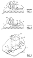
- W and S may vary from one heat spreader/footprint combination to another, depending on such factors as: the size and shape of the footprint; the type of solder paste used; the wattage, beam shape/beam width, and scan rate of the laser(s); the number of lasers used at a given time; the number N of mounting pads per footprint; the length(s) L and arrangement of the mounting pads; and so forth.
- the value of S may be very small, on the order of 0.1 to 1.0 mm.
- the pads 20 all have the same width W and the laser beam is directed along each footprint edge 31/32 at the same rate of travel, by the time the beam reaches the last pad along each edge, the last pad may have been exposed to too much energy (i.e., laser energy plus substrate-conducted thermal energy from adjacent heated pads). If this is the case, two corrections may be made: (1) slow down the beam rate of travel as the beam scans along each edge, or (2) progressively increase the width of each pad going from the first end 37 of the beamed edge 31/32 to the second end 39.
- the former correction may involve an inordinate amount of time and effort to program the laser beam travel control program to accommodate each component heat spreader; however, the latter approach is much easier to implement, and is thus the preferred approach.
- the mounting pads 20 may be constructed of conventional copper metallizations or traces, which are well known to those skilled in the art of PCB manufacture.
- the mounting pads may have a tri-metallic sandwich construction, as illustrated in FIG. 10. This construction may consist of a copper-aluminum-copper sandwich, constructed by such techniques as selective masking, plating, and etching.
- the tri-metallic constructions may comprise one or more metals other than copper and aluminum, such as nickel, iron, gold, and so forth.
- the mounting pads 20 comprise copper metallizations or tri-metal sandwich constructions
- one or more of the second portions 22 may have vias or through-holes 24 defined therethrough, as shown in FIG. 6. When used, the vias 24 may be accompanied by corresponding vias or through-holes in the underlying substrate 10 (not shown).
- the mounting pad vias 24 may be included to assist in outgassing and/or in thermal transport of heat away from the heat spreader.
Landscapes
- Engineering & Computer Science (AREA)
- Microelectronics & Electronic Packaging (AREA)
- Manufacturing & Machinery (AREA)
- Physics & Mathematics (AREA)
- Thermal Sciences (AREA)
- Electric Connection Of Electric Components To Printed Circuits (AREA)
Applications Claiming Priority (2)
| Application Number | Priority Date | Filing Date | Title |
|---|---|---|---|
| US09/058,128 US5920462A (en) | 1998-04-10 | 1998-04-10 | Heat spreader mounting pad configurations for laser soldering |
| US58128 | 1998-04-10 |
Publications (1)
| Publication Number | Publication Date |
|---|---|
| EP0949853A1 true EP0949853A1 (fr) | 1999-10-13 |
Family
ID=22014876
Family Applications (1)
| Application Number | Title | Priority Date | Filing Date |
|---|---|---|---|
| EP99302404A Withdrawn EP0949853A1 (fr) | 1998-04-10 | 1999-03-29 | Configurations de plages de montage d'un dissipateur de chaleur pour le soudage par laser |
Country Status (3)
| Country | Link |
|---|---|
| US (1) | US5920462A (fr) |
| EP (1) | EP0949853A1 (fr) |
| CA (1) | CA2268700A1 (fr) |
Families Citing this family (14)
| Publication number | Priority date | Publication date | Assignee | Title |
|---|---|---|---|---|
| US6168070B1 (en) * | 1998-10-14 | 2001-01-02 | Visteon Global Technologies, Inc. | Method for soldering DPAK-type electronic components to circuit boards |
| US6351386B1 (en) * | 2001-03-13 | 2002-02-26 | Motorola, Inc. | Component shim for mounting a component on a heat spreader |
| US6833526B2 (en) * | 2001-03-28 | 2004-12-21 | Visteon Global Technologies, Inc. | Flex to flex soldering by diode laser |
| US6680457B2 (en) * | 2002-01-15 | 2004-01-20 | Agilent Technologies, Inc. | Reflowing of solder joints |
| JP2004103849A (ja) * | 2002-09-10 | 2004-04-02 | Fuji Xerox Co Ltd | 電子部品実装基板及び電子部品交換方法 |
| US6854853B2 (en) * | 2003-03-17 | 2005-02-15 | Visteon Global Technologies, Inc. | Method for wave soldering of surface mounted light emitting diodes |
| US7967184B2 (en) * | 2005-11-16 | 2011-06-28 | Sandisk Corporation | Padless substrate for surface mounted components |
| US7696594B2 (en) * | 2005-12-22 | 2010-04-13 | International Business Machines Corporation | Attachment of a QFN to a PCB |
| US20090120916A1 (en) * | 2007-11-12 | 2009-05-14 | L3 Communications Corporation | Through-Via Laser Reflow Systems And Methods For Surface Mount Components |
| KR100924554B1 (ko) * | 2007-11-30 | 2009-11-02 | 주식회사 하이닉스반도체 | 플립 칩 패키지 및 이의 제조 방법 |
| US20120012376A1 (en) * | 2010-07-14 | 2012-01-19 | Research In Motion Limited | Assembly, and associated method, for forming a solder connection |
| US9480185B2 (en) | 2014-01-08 | 2016-10-25 | Enphase Energy, Inc. | Double insulated heat spreader |
| EP3905861A1 (fr) * | 2020-04-30 | 2021-11-03 | ZKW Group GmbH | Barrière contre le décalage des composants smt |
| CN115023037B (zh) * | 2021-09-18 | 2023-04-11 | 荣耀终端有限公司 | 电路板组件以及电子设备 |
Citations (4)
| Publication number | Priority date | Publication date | Assignee | Title |
|---|---|---|---|---|
| US4926022A (en) * | 1989-06-20 | 1990-05-15 | Digital Equipment Corporation | Laser reflow soldering process and bonded assembly formed thereby |
| US5410449A (en) * | 1993-05-24 | 1995-04-25 | Delco Electronics Corp. | Heatsink conductor solder pad |
| US5663529A (en) * | 1995-09-14 | 1997-09-02 | Ford Motor Company | Anti-skew mounting pads and processing method for electronic surface mount components |
| GB2313961A (en) * | 1996-06-08 | 1997-12-10 | Motorola Inc | Preventing dislocation of surface mounted components during soldering |
Family Cites Families (12)
| Publication number | Priority date | Publication date | Assignee | Title |
|---|---|---|---|---|
| US4760948A (en) * | 1986-12-23 | 1988-08-02 | Rca Corporation | Leadless chip carrier assembly and method |
| US5019941A (en) * | 1989-11-03 | 1991-05-28 | Motorola, Inc. | Electronic assembly having enhanced heat dissipating capabilities |
| US5315070A (en) * | 1991-12-02 | 1994-05-24 | Siemens Aktiengesellschaft | Printed wiring board to which solder has been applied |
| US5229916A (en) * | 1992-03-04 | 1993-07-20 | International Business Machines Corporation | Chip edge interconnect overlay element |
| US5221038A (en) * | 1992-10-05 | 1993-06-22 | Motorola, Inc. | Method for forming tin-indium or tin-bismuth solder connection having increased melting temperature |
| US5339218A (en) * | 1993-05-20 | 1994-08-16 | Microsemi Corporation | Surface mount device |
| US5495089A (en) * | 1993-06-04 | 1996-02-27 | Digital Equipment Corporation | Laser soldering surface mount components of a printed circuit board |
| US5504652A (en) * | 1994-09-16 | 1996-04-02 | Apple Computer, Inc. | Unitary heat sink for integrated circuits |
| US5842275A (en) * | 1995-09-05 | 1998-12-01 | Ford Motor Company | Reflow soldering to mounting pads with vent channels to avoid skewing |
| US5598321A (en) * | 1995-09-11 | 1997-01-28 | National Semiconductor Corporation | Ball grid array with heat sink |
| JP3231225B2 (ja) * | 1995-09-18 | 2001-11-19 | アルプス電気株式会社 | プリント配線基板 |
| US5764488A (en) * | 1996-06-11 | 1998-06-09 | Ast Research, Inc. | Printed circuit board having a dual pattern footprint for receiving one of two component packages |
-
1998
- 1998-04-10 US US09/058,128 patent/US5920462A/en not_active Expired - Fee Related
-
1999
- 1999-03-29 EP EP99302404A patent/EP0949853A1/fr not_active Withdrawn
- 1999-04-08 CA CA002268700A patent/CA2268700A1/fr not_active Abandoned
Patent Citations (4)
| Publication number | Priority date | Publication date | Assignee | Title |
|---|---|---|---|---|
| US4926022A (en) * | 1989-06-20 | 1990-05-15 | Digital Equipment Corporation | Laser reflow soldering process and bonded assembly formed thereby |
| US5410449A (en) * | 1993-05-24 | 1995-04-25 | Delco Electronics Corp. | Heatsink conductor solder pad |
| US5663529A (en) * | 1995-09-14 | 1997-09-02 | Ford Motor Company | Anti-skew mounting pads and processing method for electronic surface mount components |
| GB2313961A (en) * | 1996-06-08 | 1997-12-10 | Motorola Inc | Preventing dislocation of surface mounted components during soldering |
Also Published As
| Publication number | Publication date |
|---|---|
| US5920462A (en) | 1999-07-06 |
| CA2268700A1 (fr) | 1999-10-10 |
Similar Documents
| Publication | Publication Date | Title |
|---|---|---|
| US5920462A (en) | Heat spreader mounting pad configurations for laser soldering | |
| US6674018B2 (en) | Grounding terminal and mounting structure of the same on a printed circuit board | |
| US6376907B1 (en) | Ball grid array type package for semiconductor device | |
| US7916495B2 (en) | Universal solder pad | |
| EP0942636A2 (fr) | Connexion d'une plaque à circuit imprimé par soudure | |
| JP2000299549A (ja) | 回路基板 | |
| KR20010014586A (ko) | 전기 구조물 및 그의 형성방법 | |
| JPH08288637A (ja) | 電子部品および電子部品の半田付け方法 | |
| US6612023B1 (en) | Method for registering a component lead with a U-shaped metalized pad | |
| KR100895964B1 (ko) | 저 프로파일 집적 모듈 상호접속들 | |
| EP0998175A1 (fr) | Procédé pour souder des composants électroniques du type D-pak sur une plaquette de circuit imprimé | |
| KR100730273B1 (ko) | 전기 커넥터 | |
| JP3539356B2 (ja) | モジュール実装用マザーボード | |
| JPH11163044A (ja) | プリント配線板および電子部品実装方法 | |
| US5373113A (en) | Solder reflow mounting board | |
| KR100575166B1 (ko) | 반도체 패키지의 패드구조 | |
| JPH10107176A (ja) | 電子部品と基板との接続構造及びその接続方法、並びにその接続構造及び接続方法におけるはんだバンプ形成法 | |
| US4536825A (en) | Leadframe having severable fingers for aligning one or more electronic circuit device components | |
| JP3410199B2 (ja) | 接続部材の橋絡防止装置並びにこれを有する半導体集積回路及び実装基板 | |
| JPS58134454A (ja) | リ−ドボンデイング構造 | |
| JPH09312449A (ja) | 端子付き部品の取付け構造 | |
| JP3048236B2 (ja) | 電子部品 | |
| GB2378042A (en) | Fixing mechanical parts to PCBs | |
| KR20230115476A (ko) | 기판 및 기판 제조 방법 | |
| JPS6059743B2 (ja) | 半導体集積回路装置 |
Legal Events
| Date | Code | Title | Description |
|---|---|---|---|
| PUAI | Public reference made under article 153(3) epc to a published international application that has entered the european phase |
Free format text: ORIGINAL CODE: 0009012 |
|
| AK | Designated contracting states |
Kind code of ref document: A1 Designated state(s): DE ES GB |
|
| AX | Request for extension of the european patent |
Free format text: AL;LT;LV;MK;RO;SI |
|
| 17P | Request for examination filed |
Effective date: 20000226 |
|
| AKX | Designation fees paid |
Free format text: DE ES GB |
|
| STAA | Information on the status of an ep patent application or granted ep patent |
Free format text: STATUS: THE APPLICATION HAS BEEN WITHDRAWN |
|
| 18W | Application withdrawn |
Effective date: 20040523 |