EP0949855A2 - Mehrschichtige Leiterplatte - Google Patents
Mehrschichtige Leiterplatte Download PDFInfo
- Publication number
- EP0949855A2 EP0949855A2 EP99302743A EP99302743A EP0949855A2 EP 0949855 A2 EP0949855 A2 EP 0949855A2 EP 99302743 A EP99302743 A EP 99302743A EP 99302743 A EP99302743 A EP 99302743A EP 0949855 A2 EP0949855 A2 EP 0949855A2
- Authority
- EP
- European Patent Office
- Prior art keywords
- via hole
- wiring pattern
- blind via
- plated film
- exposed
- Prior art date
- Legal status (The legal status is an assumption and is not a legal conclusion. Google has not performed a legal analysis and makes no representation as to the accuracy of the status listed.)
- Granted
Links
Images



Classifications
-
- H—ELECTRICITY
- H05—ELECTRIC TECHNIQUES NOT OTHERWISE PROVIDED FOR
- H05K—PRINTED CIRCUITS; CASINGS OR CONSTRUCTIONAL DETAILS OF ELECTRIC APPARATUS; MANUFACTURE OF ASSEMBLAGES OF ELECTRICAL COMPONENTS
- H05K3/00—Apparatus or processes for manufacturing printed circuits
- H05K3/46—Manufacturing multilayer circuits
-
- H—ELECTRICITY
- H05—ELECTRIC TECHNIQUES NOT OTHERWISE PROVIDED FOR
- H05K—PRINTED CIRCUITS; CASINGS OR CONSTRUCTIONAL DETAILS OF ELECTRIC APPARATUS; MANUFACTURE OF ASSEMBLAGES OF ELECTRICAL COMPONENTS
- H05K3/00—Apparatus or processes for manufacturing printed circuits
- H05K3/40—Forming printed elements for providing electric connections to or between printed circuits
- H05K3/42—Plated through-holes or plated via connections
- H05K3/423—Plated through-holes or plated via connections characterised by electroplating method
-
- H—ELECTRICITY
- H05—ELECTRIC TECHNIQUES NOT OTHERWISE PROVIDED FOR
- H05K—PRINTED CIRCUITS; CASINGS OR CONSTRUCTIONAL DETAILS OF ELECTRIC APPARATUS; MANUFACTURE OF ASSEMBLAGES OF ELECTRICAL COMPONENTS
- H05K3/00—Apparatus or processes for manufacturing printed circuits
- H05K3/0011—Working of insulating substrates or insulating layers
- H05K3/0017—Etching of the substrate by chemical or physical means
- H05K3/0026—Etching of the substrate by chemical or physical means by laser ablation
- H05K3/0032—Etching of the substrate by chemical or physical means by laser ablation of organic insulating material
- H05K3/0035—Etching of the substrate by chemical or physical means by laser ablation of organic insulating material of blind holes, i.e. having a metal layer at the bottom
-
- H—ELECTRICITY
- H05—ELECTRIC TECHNIQUES NOT OTHERWISE PROVIDED FOR
- H05K—PRINTED CIRCUITS; CASINGS OR CONSTRUCTIONAL DETAILS OF ELECTRIC APPARATUS; MANUFACTURE OF ASSEMBLAGES OF ELECTRICAL COMPONENTS
- H05K3/00—Apparatus or processes for manufacturing printed circuits
- H05K3/46—Manufacturing multilayer circuits
- H05K3/4644—Manufacturing multilayer circuits by building the multilayer layer by layer, i.e. build-up multilayer circuits
-
- H—ELECTRICITY
- H05—ELECTRIC TECHNIQUES NOT OTHERWISE PROVIDED FOR
- H05K—PRINTED CIRCUITS; CASINGS OR CONSTRUCTIONAL DETAILS OF ELECTRIC APPARATUS; MANUFACTURE OF ASSEMBLAGES OF ELECTRICAL COMPONENTS
- H05K3/00—Apparatus or processes for manufacturing printed circuits
- H05K3/46—Manufacturing multilayer circuits
- H05K3/4644—Manufacturing multilayer circuits by building the multilayer layer by layer, i.e. build-up multilayer circuits
- H05K3/4652—Adding a circuit layer by laminating a metal foil or a preformed metal foil pattern
-
- H—ELECTRICITY
- H05—ELECTRIC TECHNIQUES NOT OTHERWISE PROVIDED FOR
- H05K—PRINTED CIRCUITS; CASINGS OR CONSTRUCTIONAL DETAILS OF ELECTRIC APPARATUS; MANUFACTURE OF ASSEMBLAGES OF ELECTRICAL COMPONENTS
- H05K1/00—Printed circuits
- H05K1/02—Details
- H05K1/11—Printed elements for providing electric connections to or between printed circuits
- H05K1/115—Via connections; Lands around holes or via connections
- H05K1/116—Lands, clearance holes or other lay-out details concerning the surrounding of a via
-
- H—ELECTRICITY
- H05—ELECTRIC TECHNIQUES NOT OTHERWISE PROVIDED FOR
- H05K—PRINTED CIRCUITS; CASINGS OR CONSTRUCTIONAL DETAILS OF ELECTRIC APPARATUS; MANUFACTURE OF ASSEMBLAGES OF ELECTRICAL COMPONENTS
- H05K2201/00—Indexing scheme relating to printed circuits covered by H05K1/00
- H05K2201/09—Shape and layout
- H05K2201/09209—Shape and layout details of conductors
- H05K2201/095—Conductive through-holes or vias
- H05K2201/09509—Blind vias, i.e. vias having one side closed
-
- H—ELECTRICITY
- H05—ELECTRIC TECHNIQUES NOT OTHERWISE PROVIDED FOR
- H05K—PRINTED CIRCUITS; CASINGS OR CONSTRUCTIONAL DETAILS OF ELECTRIC APPARATUS; MANUFACTURE OF ASSEMBLAGES OF ELECTRICAL COMPONENTS
- H05K2201/00—Indexing scheme relating to printed circuits covered by H05K1/00
- H05K2201/09—Shape and layout
- H05K2201/09209—Shape and layout details of conductors
- H05K2201/095—Conductive through-holes or vias
- H05K2201/09563—Metal filled via
-
- H—ELECTRICITY
- H05—ELECTRIC TECHNIQUES NOT OTHERWISE PROVIDED FOR
- H05K—PRINTED CIRCUITS; CASINGS OR CONSTRUCTIONAL DETAILS OF ELECTRIC APPARATUS; MANUFACTURE OF ASSEMBLAGES OF ELECTRICAL COMPONENTS
- H05K2201/00—Indexing scheme relating to printed circuits covered by H05K1/00
- H05K2201/09—Shape and layout
- H05K2201/09209—Shape and layout details of conductors
- H05K2201/09654—Shape and layout details of conductors covering at least two types of conductors provided for in H05K2201/09218 - H05K2201/095
- H05K2201/0969—Apertured conductors
-
- H—ELECTRICITY
- H05—ELECTRIC TECHNIQUES NOT OTHERWISE PROVIDED FOR
- H05K—PRINTED CIRCUITS; CASINGS OR CONSTRUCTIONAL DETAILS OF ELECTRIC APPARATUS; MANUFACTURE OF ASSEMBLAGES OF ELECTRICAL COMPONENTS
- H05K2201/00—Indexing scheme relating to printed circuits covered by H05K1/00
- H05K2201/09—Shape and layout
- H05K2201/09209—Shape and layout details of conductors
- H05K2201/09654—Shape and layout details of conductors covering at least two types of conductors provided for in H05K2201/09218 - H05K2201/095
- H05K2201/098—Special shape of the cross-section of conductors, e.g. very thick plated conductors
-
- H—ELECTRICITY
- H05—ELECTRIC TECHNIQUES NOT OTHERWISE PROVIDED FOR
- H05K—PRINTED CIRCUITS; CASINGS OR CONSTRUCTIONAL DETAILS OF ELECTRIC APPARATUS; MANUFACTURE OF ASSEMBLAGES OF ELECTRICAL COMPONENTS
- H05K2201/00—Indexing scheme relating to printed circuits covered by H05K1/00
- H05K2201/09—Shape and layout
- H05K2201/09818—Shape or layout details not covered by a single group of H05K2201/09009 - H05K2201/09809
- H05K2201/09827—Tapered, e.g. tapered hole, via or groove
-
- H—ELECTRICITY
- H05—ELECTRIC TECHNIQUES NOT OTHERWISE PROVIDED FOR
- H05K—PRINTED CIRCUITS; CASINGS OR CONSTRUCTIONAL DETAILS OF ELECTRIC APPARATUS; MANUFACTURE OF ASSEMBLAGES OF ELECTRICAL COMPONENTS
- H05K2203/00—Indexing scheme relating to apparatus or processes for manufacturing printed circuits covered by H05K3/00
- H05K2203/11—Treatments characterised by their effect, e.g. heating, cooling, roughening
- H05K2203/1152—Replicating the surface structure of a sacrificial layer, e.g. for roughening
-
- H—ELECTRICITY
- H05—ELECTRIC TECHNIQUES NOT OTHERWISE PROVIDED FOR
- H05K—PRINTED CIRCUITS; CASINGS OR CONSTRUCTIONAL DETAILS OF ELECTRIC APPARATUS; MANUFACTURE OF ASSEMBLAGES OF ELECTRICAL COMPONENTS
- H05K3/00—Apparatus or processes for manufacturing printed circuits
- H05K3/10—Apparatus or processes for manufacturing printed circuits in which conductive material is applied to the insulating support in such a manner as to form the desired conductive pattern
- H05K3/108—Apparatus or processes for manufacturing printed circuits in which conductive material is applied to the insulating support in such a manner as to form the desired conductive pattern by semi-additive methods; masks therefor
-
- H—ELECTRICITY
- H05—ELECTRIC TECHNIQUES NOT OTHERWISE PROVIDED FOR
- H05K—PRINTED CIRCUITS; CASINGS OR CONSTRUCTIONAL DETAILS OF ELECTRIC APPARATUS; MANUFACTURE OF ASSEMBLAGES OF ELECTRICAL COMPONENTS
- H05K3/00—Apparatus or processes for manufacturing printed circuits
- H05K3/38—Improvement of the adhesion between the insulating substrate and the metal
- H05K3/381—Improvement of the adhesion between the insulating substrate and the metal by special treatment of the substrate
Definitions
- the present invention relates to a process for producing a multilayer circuit board and, more particularly, to a process for producing a multilayer circuit board having a blind via hole which is filled with plated film.
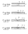
- Figs. 5(a) to 5(c) shows one of the known processes for producing a multilayer circuit board.
- a metal foil such as a copper foil or the like, with an adhesive resin layer, such as a pre-preg or polyimide resin layer, is laminated and heat-pressed so that the metal foil 16 is adhered onto the resin base 12, as shown in Figs. 5(a) and 5(b).
- a blind via hole 18 is formed by a carbon dioxide gas laser through the metal foil 16 and the resin layer 14 so that a part of the wiring pattern 10 is exposed, as shown in Fig. 5(c).
- an electroless-copper plating or electro-copper plating is applied to the blind via hole 18 to form a plated film 20 to attain an electrical connection between the wiring pattern 10 and the metal foil 16, as shown in Fig. 5(d).
- the metal foil 16 is etched to form a predetermined wiring pattern (not shown).
- Figs. 6(a) and 6(b) show another known process for producing a multilayer circuit board.
- a photosensitive resin layer 22 is formed, as shown in Fig. 6(a).
- the photosensitive resin layer 22 is etched by a photolithographic method to form a blind via hole 24 which reaches to a circuit pattern, a plated film 26 is formed on the blind via hole 24 and the resin layer 22 by a sputtering process and an electro-plating process, as shown in Fig. 6(c), and the plated film formed on the resin layer 22 is etched to form a desired circuit pattern.
- the blind via hole 18 is generally formed by a carbon dioxide laser as mentioned above.
- a carbon dioxide laser is limited to form a hole, the diameter thereof being 80 ⁇ m or more. Consequently, it is impossible to form such a via hole, the diameter thereof being less than 80 ⁇ m, using a carbon dioxide laser.
- the electric current may be concentrated at the angle portion A of the metal foil 16, i.e., an inlet edge of the blind via hole 18.
- the inlet edge of the blind via hole 18 may become "necked", the diameter of the inlet portion being narrow, and the plating liquid may enter therein and affectedly influence the plated film.
- the diameter deep inside the blind via hole 18 becomes relatively large and the thickness of the plated layer becomes thin. Thus, an electrical disconnection may occur in the blind via hole.
- An object of the present invention is to provide a process for producing a multilayer circuit board in which a blind via hole of a small diameter can be made and high density wiring can be provided.
- Another object of the present invention is to provide a process for producing a multilayer circuit board in which the above-mentioned drawbacks can be overcome.
- a process for producing a multilayer wiring board comprising the following steps of: laminating an electrically insulating resin substrate, having first and second surfaces and a metal layer formed on the first surface, onto a base material on which a predetermined wiring pattern is formed, so that the second surface of the resin substrate is adhered to the base material; removing a predetermined range of the metal layer to form an opening at a position where a connection with the wiring pattern is to be provided; irradiating a laser beam toward the resin layer through the resin removed region to form a blind via hole having a diameter smaller than that of the opening, so that the wiring pattern is exposed at a bottom of the blind via hole; electroless plating to form an electroless plated film on the exposed wiring pattern, a side wall of the blind via hole, a step portion of the exposed resin layer, and at least a metal layer at a periphery of the opening; electro plating to form an electro plated film on the electroless plated film; and after the electro plating,
- the laser beam irradiating step comprises a step of irradiating a laser beam having a wavelength in the ultraviolet range.
- a process for producing a multilayer wiring board comprising the following steps of: forming a resin layer onto an electrically insulating base material on which a predetermined wiring pattern is formed; adhering a metal layer onto the resin layer; removing a predetermined amount of the metal layer to form an opening at a position where a connection with the wiring pattern is to be attained; irradiating a laser beam toward the resin layer through the resin removed region to form a blind via hole having a diameter smaller than that of the opening, so that the wiring pattern is exposed at a bottom of the blind via hole; electroless plating to form an electroless plated film on the exposed wiring pattern, a side wall of the blind via hole, a step portion of the exposed resin layer, and at least a metal layer at a periphery of the opening; electro plating to form an electro plated film on the electroless plated film; and after the electro plating, etching the metal layer to form a predetermined wiring pattern.
- a process for producing a multilayer wiring board comprising the following steps of: laminating an electrically insulating resin substrate onto a base material on which a predetermined wiring pattern is formed, so that a surface of the resin substrate covers the wiring pattern; irradiating a laser beam toward the resin layer to form a blind via hole, so that the wiring pattern is exposed at a bottom of the blind via hole; electroless plating to form an electroless plated film on the exposed wiring pattern and a side wall of the blind via hole; forming a resist on the electroless plated film except for the region of the via hole and a peripheral area thereof; electro plating to form an electro plated film on the electroless plated film except for the resist; and removing the resist and subsequently the electroless plated film under the resist.
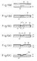
- Figs. 1(a) to 1(f) show a first embodiment of this invention.
- a circuit pattern 30 is formed on the base substrate 32 (a printed circuit board, a ceramic circuit board, or the like).
- a resin substrate with metal foil which comprises an adhesive resin layer 34, such as a pre-preg, a polyimide resin layer or the like, formed on one surface of a metal foil 36, such as a copper foil, is laminated on the circuit pattern 30, as shown in Fig. 1(a).
- the resin layer 34 is then pressed and heated to harden the same so that the substrate 32 is adhered to the metal foil 36 through the resin layer 34.
- the metal foil 36 at the portion of the lands corresponding to the connecting portion of the blind via connecting portion is removed by an etching process or a laser process to form an opening 38 so that a part of resin layer 34 is exposed, as shown in Fig. 1(c).
- the diameter X of the opening 38 is smaller than the diameter C of the land of the wiring pattern 30.
- the position of the opening 38 is made as connecting portion between the upper and lower wiring patterns. Since the diameter of this connecting portion is smaller than the diameter C of the land, the wiring density thereof is not affected and high density wiring can thus be attained.
- a resin substrate with metal foil in which an opening is beforehand provided at a position of the metal foil corresponding to the lands of the wiring pattern, can also be laminated with each other.
- a blind via hole 40 is formed at a position of the resin layer 34 at which the resin layer 34 is exposed and the exposed portion becomes the bottom of the blind via hole 30, as shown in Fig. 1(d).
- the diameter of the blind via hole 40 is smaller than that of the opening 38.
- the blind via hole 40 can be formed by a laser process.
- a carbon dioxide laser is not suitable since it is difficult to bore a hole having a diameter of less than 80 ⁇ m by a carbon dioxide laser.
- a mask i.e., a metal mask, can be used to form such a hole having a small diameter, the productivity of such method is relatively now.
- a YAG laser or IRF laser without using any masking, to bore a hole which has a diameter of more or less 30 ⁇ m, in which the wavelength is in the ultraviolet range so as to reduce the diameter thereof.
- the carbon chain of the resin layer 34 can be cut so that the resin layer 34 is resolved and removed by irradiating a laser beam having wavelength in the ultraviolet range.
- the laser beam can be reduced to a small beam diameter and the diameter of the opening 38 can be made larger within the range of the land of the wiring pattern.
- the alignment when the laser beam is irradiated, can easily be performed. Since the diameter of the blind via hole 40 is smaller than the diameter of the opening 38, a step portion 42 of the resin layer 34 can thus remain around the periphery of the opening of the blind via hole 40.
- an electroless plated layer such as a copper layer, is formed on the surface of the wiring pattern 30, the side wall of the blind via hole 40, the exposed step portion 42 of the resin layer 34 and at least the surface of the metal foil 36, such as copper foil around the opening 38. Then, an electro plated layer 44 is formed on this electroless plated layer, as shown in Fig. 1(e).
- a predetermined wiring pattern 36a is formed by etching the metal foil 36.
- the diameter of the opening 38 is larger than the diameter of the blind via hole 40 and, therefore, the step portion 42 remains on the resin layer 34.
- the edge of the opening 38 of the metal foil 36 is removed from the opening edge of the via hole 40 and, therefore, when an electroplated film 44 is formed, even if the electric current is concentrated to the corner portion of the metal foil 36 at the edge of the opening 38 and, thus, the thickness of the plated film at the corner portion becomes larger, the recess comprising the opening 38 and the blind via hole 40 does not become a "neck", different from the prior art shown in Fig. 3. Since the inlet portion is wide open, the plating liquid does not remain in the recess and the flow of the plating liquid can be maintained. Therefore, the plated film can be formed smoothly even at the bottom portion of the via hole 40.
- Figs. 2(a) and 2(b) show a second embodiment of this invention.
- a base material such as a printed circuit board on which a circuit pattern 30 is formed
- a resin such as a polyimide resin
- This resin layer 34 can also be formed on the base material by laminating a resin film.
- a metal foil 36 is adhered onto the resin layer 34 by means of an adhesive.
- an electroless copper plating is conducted and then an electro copper plated film 44 is formed as shown in Fig. 1(e).
- the blind via hole 40 could be substantially covered by the electro-copper plated film 44, as shown in Fig. 3. That is to say, the density of electric current when conducting the electro copper plating could be reduced to less than an ordinary density of electric current (2 to 3 ASD).
- the inside area of the blind via hole 40 restricts a flow of the plating material more than a flat surface, such as a surface of the conductive layer 36 formed on the resin layer 34.
- a flat surface such as a surface of the conductive layer 36 formed on the resin layer 34.
- the density of electric current could be reduced by 0.1 to 2 ADS, preferably by around 1 ADS, the difference in the plating deposition speed between the flat surface and the inside of the blind via hole 40 was uniform, or otherwise the plating deposition speed at the blind via hole 40 was higher than that on the flat surface.
- the plating film can heap up not only at the bottom surface of the blind via hole 40, but also at the side surface thereof. Therefore, the thickness t 2 of the plated film from the bottom becomes larger than the thickness t 1 of the plated film at the flat surface and therefore it is possible to completely cover the blind via hole 40.
- the blind via hole 40 could finally be covered completely with the plated film.
- the diameter of the opening of the blind via hole 40 was 50 ⁇ m and the depth thereof was 40 ⁇ m, in which the thickness of the metal foil 36 (the thickness thereof being 5 ⁇ m) and the thickness t 1 of the plated film (the sum of the thickness of the electroless plated film and the thickness of the electro plated film) was 20 ⁇ m, the inside of the blind via hole 40 could substantially be covered by the plated film.
- the most important factor is to reduce the density of electric current in the process of electro plating.
- the blind via hole 40 is tapered in such a manner that the inlet portion thereof is enlarged, since the plating liquid can circulate easily and deposition efficiency is improved.
- the aspect ratio h/r was preferably 0.5 to 1.5.
- a plated film having a thickness t 2 of the plated film can be obtained, in which t 2 satisfies the above conditions.
- the diameter r of the opening of the blind via hole 40 is preferably 20 to 100 ⁇ m and the depth h thereof is preferably 20 to 100 ⁇ m. Therefore, the aspect ratio h/r is preferably 0.5 to 1.5 as mentioned above.
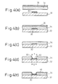
- Figs. 4(a) to 4(i) show a process for producing a multilayer wiring board of still another embodiment according to the present invention.
- Figs. 4(a) and 4(b) corresponds to Fig. 1(a) and 1(b), respectively, and therefore a detailed explanation is omitted.
- Fig. 4(c) the copper foil 36 is completely removed from the upper surface of the adhesive resin layer 34. Then, a blind via hole 40 is formed by a laser process at a position of the resin layer 34 by which the resin layer 34 is exposed and the exposed portion becomes a bottom of the blind via hole 40, as shown in Fig. 4(d).
- an electroless plated layer 46 such as a copper layer, is formed on the surface of the wiring pattern 30, the side wall of the blind via hole 40, the surface of the resin layer 34 around the blind via hole 40, as shown in Fig. 4(d).
- a resist 48 is formed on the resin layer 34 except for the area of the blind via hole 40 and the peripheral region thereof, as shown in Fig. 4(f).
- an electro plated layer 44 is formed on this electroless plated layer, except for the area covered by the resist 48, as shown in Fig. 4(g).
- the resist 48 is removed by a known process, as shown in Fig. 4(h) and also the electroless plated layer 46 is removed by etching, as shown in Fig. 4(i).
Landscapes
- Engineering & Computer Science (AREA)
- Manufacturing & Machinery (AREA)
- Microelectronics & Electronic Packaging (AREA)
- Physics & Mathematics (AREA)
- Optics & Photonics (AREA)
- Production Of Multi-Layered Print Wiring Board (AREA)
- Printing Elements For Providing Electric Connections Between Printed Circuits (AREA)
Applications Claiming Priority (4)
| Application Number | Priority Date | Filing Date | Title |
|---|---|---|---|
| JP9906798 | 1998-04-10 | ||
| JP9906798 | 1998-04-10 | ||
| JP31295898 | 1998-11-04 | ||
| JP31295898 | 1998-11-04 |
Publications (3)
| Publication Number | Publication Date |
|---|---|
| EP0949855A2 true EP0949855A2 (de) | 1999-10-13 |
| EP0949855A3 EP0949855A3 (de) | 2000-10-18 |
| EP0949855B1 EP0949855B1 (de) | 2006-05-31 |
Family
ID=26440222
Family Applications (1)
| Application Number | Title | Priority Date | Filing Date |
|---|---|---|---|
| EP99302743A Expired - Lifetime EP0949855B1 (de) | 1998-04-10 | 1999-04-08 | Verfahren zur Herstellung einer mit elektroplattiertem Sackloch versehenen mehrschichtige Leiterplatte |
Country Status (3)
| Country | Link |
|---|---|
| EP (1) | EP0949855B1 (de) |
| KR (1) | KR100336829B1 (de) |
| DE (1) | DE69931551T2 (de) |
Cited By (4)
| Publication number | Priority date | Publication date | Assignee | Title |
|---|---|---|---|---|
| WO2002011503A1 (fr) * | 2000-07-27 | 2002-02-07 | Kermel | Procede de realisation d'une circuiterie comportant pistes, pastilles et microtraversees conductrices et utilisation de ce procede pour la realisation de circuits imprimes et de modules multicouches a haute densite d'integration |
| EP1122989A3 (de) * | 2000-02-01 | 2002-07-03 | Shinko Electric Industries Co. Ltd. | Plattierungsverfahren zum Füllen von Kontaktlöchern |
| US7243425B2 (en) * | 2004-12-24 | 2007-07-17 | Cmk Corporation | Printed wiring board and method of manufacturing the same |
| CN106507611A (zh) * | 2015-09-07 | 2017-03-15 | 欣兴电子股份有限公司 | 线路板的制造方法 |
Families Citing this family (2)
| Publication number | Priority date | Publication date | Assignee | Title |
|---|---|---|---|---|
| KR100791353B1 (ko) * | 2005-05-20 | 2008-01-07 | 삼성전기주식회사 | 영구보호피막의 형성방법 및 영구보호피막이 형성된인쇄회로기판 |
| KR100730782B1 (ko) * | 2006-04-13 | 2007-06-20 | (주)인터플렉스 | Uv-co2레이저를 이용한 연성회로기판 제조방법 |
Family Cites Families (6)
| Publication number | Priority date | Publication date | Assignee | Title |
|---|---|---|---|---|
| US3350498A (en) * | 1965-01-04 | 1967-10-31 | Intellux Inc | Multilayer circuit and method of making the same |
| EP0164564A1 (de) * | 1984-05-18 | 1985-12-18 | Siemens Aktiengesellschaft | Anordnung zur Sacklocherzeugung in einem laminierten Aufbau |
| US4642160A (en) * | 1985-08-12 | 1987-02-10 | Interconnect Technology Inc. | Multilayer circuit board manufacturing |
| JPH03173497A (ja) * | 1989-12-01 | 1991-07-26 | Hitachi Cable Ltd | 多層配線基板およびその製造方法 |
| JP3785223B2 (ja) * | 1996-06-10 | 2006-06-14 | エルナー株式会社 | 多層プリント配線板の製造方法 |
| JPH1027960A (ja) * | 1996-07-09 | 1998-01-27 | Mitsui Mining & Smelting Co Ltd | 多層プリント配線板の製造方法 |
-
1999
- 1999-02-06 KR KR1019990004071A patent/KR100336829B1/ko not_active Expired - Fee Related
- 1999-04-08 EP EP99302743A patent/EP0949855B1/de not_active Expired - Lifetime
- 1999-04-08 DE DE69931551T patent/DE69931551T2/de not_active Expired - Lifetime
Cited By (5)
| Publication number | Priority date | Publication date | Assignee | Title |
|---|---|---|---|---|
| EP1122989A3 (de) * | 2000-02-01 | 2002-07-03 | Shinko Electric Industries Co. Ltd. | Plattierungsverfahren zum Füllen von Kontaktlöchern |
| US6755957B2 (en) | 2000-02-01 | 2004-06-29 | Shinko Electric Industries Co., Ltd. | Method of plating for filling via holes |
| WO2002011503A1 (fr) * | 2000-07-27 | 2002-02-07 | Kermel | Procede de realisation d'une circuiterie comportant pistes, pastilles et microtraversees conductrices et utilisation de ce procede pour la realisation de circuits imprimes et de modules multicouches a haute densite d'integration |
| US7243425B2 (en) * | 2004-12-24 | 2007-07-17 | Cmk Corporation | Printed wiring board and method of manufacturing the same |
| CN106507611A (zh) * | 2015-09-07 | 2017-03-15 | 欣兴电子股份有限公司 | 线路板的制造方法 |
Also Published As
| Publication number | Publication date |
|---|---|
| EP0949855B1 (de) | 2006-05-31 |
| DE69931551D1 (de) | 2006-07-06 |
| DE69931551T2 (de) | 2006-10-12 |
| KR100336829B1 (ko) | 2002-05-16 |
| KR19990082699A (ko) | 1999-11-25 |
| EP0949855A3 (de) | 2000-10-18 |
Similar Documents
| Publication | Publication Date | Title |
|---|---|---|
| US5369881A (en) | Method of forming circuit wiring pattern | |
| EP0843955B1 (de) | Verfahren zur herstellung von erhöhten metallischen kontakten auf elektrischen schaltungen | |
| US6618940B2 (en) | Fine pitch circuitization with filled plated through holes | |
| EP1102525B1 (de) | Gedruckte leiterplatte und verfahren zu deren herstellung | |
| US5733466A (en) | Electrolytic method of depositing gold connectors on a printed circuit board | |
| KR100427794B1 (ko) | 다층 배선 기판의 제조 방법 | |
| US20020083586A1 (en) | Process for producing multilayer circuit board | |
| US9744624B2 (en) | Method for manufacturing circuit board | |
| US6977349B2 (en) | Method for manufacturing wiring circuit boards with bumps and method for forming bumps | |
| US7080448B2 (en) | PCB with inlaid outer-layer circuits and production methods thereof | |
| EP0949855B1 (de) | Verfahren zur Herstellung einer mit elektroplattiertem Sackloch versehenen mehrschichtige Leiterplatte | |
| EP1049364A1 (de) | Verfahren zur herstellung mehrschichtiger verbindungsplatten | |
| JP2004146742A (ja) | 配線基板の製造方法 | |
| JPH11195849A (ja) | フレキシブルプリント配線板とその製造方法 | |
| KR20020026849A (ko) | 범프가 부착된 배선회로 기판 및 그 제조방법 | |
| KR100351923B1 (ko) | 인쇄회로기판 제조방법 | |
| JP2000200975A (ja) | 多層配線基板の製造方法 | |
| KR100274662B1 (ko) | 다층 인쇄 회로 기판의 층간 비아 제조 방법 | |
| JPH1117340A (ja) | ブラインドスルーホールの形成方法 | |
| JP3275378B2 (ja) | プリント配線板の製造方法 | |
| JPH03245593A (ja) | プリント配線板の製造方法 | |
| KR100916649B1 (ko) | 인쇄회로기판의 제조방법 | |
| JP3130707B2 (ja) | プリント基板およびその製造方法 | |
| US20020045135A1 (en) | Method for manufacturing circuit board having conductive via | |
| JPH0548246A (ja) | フレキシブルプリント配線板の製造方法 |
Legal Events
| Date | Code | Title | Description |
|---|---|---|---|
| PUAI | Public reference made under article 153(3) epc to a published international application that has entered the european phase |
Free format text: ORIGINAL CODE: 0009012 |
|
| AK | Designated contracting states |
Kind code of ref document: A2 Designated state(s): DE GB |
|
| AX | Request for extension of the european patent |
Free format text: AL;LT;LV;MK;RO;SI |
|
| PUAL | Search report despatched |
Free format text: ORIGINAL CODE: 0009013 |
|
| AK | Designated contracting states |
Kind code of ref document: A3 Designated state(s): AT BE CH CY DE DK ES FI FR GB GR IE IT LI LU MC NL PT SE |
|
| AX | Request for extension of the european patent |
Free format text: AL;LT;LV;MK;RO;SI |
|
| 17P | Request for examination filed |
Effective date: 20010417 |
|
| AKX | Designation fees paid |
Free format text: DE GB |
|
| 17Q | First examination report despatched |
Effective date: 20050519 |
|
| GRAP | Despatch of communication of intention to grant a patent |
Free format text: ORIGINAL CODE: EPIDOSNIGR1 |
|
| RTI1 | Title (correction) |
Free format text: PROCESS FOR PRODUCING A MULTILAYER CIRCUIT BOARD HAVING AN ELECTROPLATED BLIND HOLE |
|
| RIN1 | Information on inventor provided before grant (corrected) |
Inventor name: KATAGIRI, NORITAKA, C/O SHINKO ELEC. IND.CO., LTD. Inventor name: KOYAMA, TOSHINORI, C/O SHINKO ELEC. IND. CO., LTD. Inventor name: NOMURA, TOMOHIRO, C/O SHINKO ELEC. IND. CO., LTD. Inventor name: IIJIMA, TAKAHIRO, C/O SHINKO ELEC. IND. CO., LTD. Inventor name: ROKUGAWA, AKIO, C/O SHINKO ELEC. IND. CO., LTD. |
|
| GRAS | Grant fee paid |
Free format text: ORIGINAL CODE: EPIDOSNIGR3 |
|
| GRAA | (expected) grant |
Free format text: ORIGINAL CODE: 0009210 |
|
| AK | Designated contracting states |
Kind code of ref document: B1 Designated state(s): DE GB |
|
| REG | Reference to a national code |
Ref country code: GB Ref legal event code: FG4D |
|
| REF | Corresponds to: |
Ref document number: 69931551 Country of ref document: DE Date of ref document: 20060706 Kind code of ref document: P |
|
| PLBE | No opposition filed within time limit |
Free format text: ORIGINAL CODE: 0009261 |
|
| STAA | Information on the status of an ep patent application or granted ep patent |
Free format text: STATUS: NO OPPOSITION FILED WITHIN TIME LIMIT |
|
| 26N | No opposition filed |
Effective date: 20070301 |
|
| PGFP | Annual fee paid to national office [announced via postgrant information from national office to epo] |
Ref country code: GB Payment date: 20110406 Year of fee payment: 13 |
|
| GBPC | Gb: european patent ceased through non-payment of renewal fee |
Effective date: 20120408 |
|
| PG25 | Lapsed in a contracting state [announced via postgrant information from national office to epo] |
Ref country code: GB Free format text: LAPSE BECAUSE OF NON-PAYMENT OF DUE FEES Effective date: 20120408 |
|
| PGFP | Annual fee paid to national office [announced via postgrant information from national office to epo] |
Ref country code: DE Payment date: 20140430 Year of fee payment: 16 |
|
| REG | Reference to a national code |
Ref country code: DE Ref legal event code: R119 Ref document number: 69931551 Country of ref document: DE |
|
| PG25 | Lapsed in a contracting state [announced via postgrant information from national office to epo] |
Ref country code: DE Free format text: LAPSE BECAUSE OF NON-PAYMENT OF DUE FEES Effective date: 20151103 |