EP0950974B1 - Lecteur de carte à puce compact et installable verticalement - Google Patents
Lecteur de carte à puce compact et installable verticalement Download PDFInfo
- Publication number
- EP0950974B1 EP0950974B1 EP98102950A EP98102950A EP0950974B1 EP 0950974 B1 EP0950974 B1 EP 0950974B1 EP 98102950 A EP98102950 A EP 98102950A EP 98102950 A EP98102950 A EP 98102950A EP 0950974 B1 EP0950974 B1 EP 0950974B1
- Authority
- EP
- European Patent Office
- Prior art keywords
- plastics
- base plate
- circuit board
- cover plate
- printed circuit
- Prior art date
- Legal status (The legal status is an assumption and is not a legal conclusion. Google has not performed a legal analysis and makes no representation as to the accuracy of the status listed.)
- Expired - Lifetime
Links
Images

Classifications
-
- G—PHYSICS
- G06—COMPUTING OR CALCULATING; COUNTING
- G06K—GRAPHICAL DATA READING; PRESENTATION OF DATA; RECORD CARRIERS; HANDLING RECORD CARRIERS
- G06K7/00—Methods or arrangements for sensing record carriers, e.g. for reading patterns
- G06K7/0013—Methods or arrangements for sensing record carriers, e.g. for reading patterns by galvanic contacts, e.g. card connectors for ISO-7816 compliant smart cards or memory cards, e.g. SD card readers
- G06K7/0021—Methods or arrangements for sensing record carriers, e.g. for reading patterns by galvanic contacts, e.g. card connectors for ISO-7816 compliant smart cards or memory cards, e.g. SD card readers for reading/sensing record carriers having surface contacts
-
- Y—GENERAL TAGGING OF NEW TECHNOLOGICAL DEVELOPMENTS; GENERAL TAGGING OF CROSS-SECTIONAL TECHNOLOGIES SPANNING OVER SEVERAL SECTIONS OF THE IPC; TECHNICAL SUBJECTS COVERED BY FORMER USPC CROSS-REFERENCE ART COLLECTIONS [XRACs] AND DIGESTS
- Y10—TECHNICAL SUBJECTS COVERED BY FORMER USPC
- Y10S—TECHNICAL SUBJECTS COVERED BY FORMER USPC CROSS-REFERENCE ART COLLECTIONS [XRACs] AND DIGESTS
- Y10S439/00—Electrical connectors
- Y10S439/945—Adapter for pcb or cartridge
Definitions
- the invention relates to a contacting unit according to the PCMCIA standard, with a card-shaped printed circuit board with electronic assemblies, in addition to the one of the narrow card sides arranged connector strip of the Printed circuit board with a contact field on a surface of the printed circuit board for the Contacting a chip card that is parallel to the circuit board an insertion slot can be inserted into a slot-like insertion channel, which is formed between a base plate and the circuit board and a Slide-in guide on the narrow one opposite the connector strip Has side, the circuit board is held by a plastic frame, the is arranged on a cover plate.
- the invention further relates to a method for the manufacture of such a contacting unit.
- a contacting unit of the type described from the German Utility model 296 07 253 known There is a card-shaped Support element according to the PCMCIA standard in a bowl-shaped housing arranged and thus in the corresponding slot of a computer, especially a notebook, insertable, the electrical contacting made in accordance with the standard via the connector strip arranged on the front becomes.
- the housing of the known contact unit is provided, one parallel to the circuit board in a slot-like insertion channel of the housing to insert the insertable chip card and by means of a to read the surface of the printed circuit board arranged contact field.
- the invention has for its object to provide a fully retractable chip card reader in the receiving slot of the computer, which can be fully inserted into the PCMCIA slot without protruding parts, although despite the shortening a safe insertion for the chip card should be given and also the mechanical stability remains guaranteed with easier manufacturability.
- the length and width of the PCMCIA standard Type II essentially corresponds and which is fully in the PCMCIA slot a computer, in particular notebooks, can be used without protruding parts remain free. Because of the full retractability contact security for the reader is improved and is any Risk of damage also avoided during transport, whereby in known manner, a protective flap can be provided, which The slot is closed when the reader is inserted.
- An essential core idea of the invention is on the base plate and to provide the cover plate with upstanding and inwardly bent staples, which are sprayed with the plastic elements to form a composite unit and over a plastic connection technology including the electronic components an extremely short and stable unit.
- the number and arrangement complement each other the staples on the base and cover plates together.
- the plastic elements of the cover plate and the base plate are preferably with corresponding positioning projections and recesses as well
- Lanyards, such as adhesive surfaces or energy direction sensors for one Provide ultrasonic welding. Simplification of assembly as well as This increases the strength of the reader.
- the plastic profile part is advantageously in one piece and essentially has a U-shaped cross-section, with the open side of the U-shape Insert slot that forms the opposite area of the U-shape in one reaches through the chip card corresponding width, above the thus formed Opening is provided in one piece, the platform-like extension, which for level mounting of the circuit board is provided with recesses in the Engage the protruding positioning tabs of the PCB flush. This is ensures that a free recording channel for the chip card is provided and your chip field securely inserted the contact field of the circuit board Condition contacted.
- the plastic holders of the base plate are advantageously as Axial stops to limit the insertion of the chip card and thus to exact positioning.
- Embodiment of the invention proposed to the U-shaped plastic frame to form its closed side only in the form of a narrow bar that corresponds to the platform-like expansion of the plastic profile part.
- the free leg ends of the plastic frame can also be used with advantage corresponding to the design of the plastic holder of the base plate be trained to position and connect the parts to simplify with each other and on the other hand the mounting of the PCMCIA connector strip to improve in the housing.
- the base plate is on the inside by a thin reinforcement plate made of metal or plastic, if necessary with spring action, reinforced, for example glued or welded can be or injected from plastic in combination with the other plastic parts can be.
- the encapsulation of the Metal staples and clamps with the various plastic profiles secure the Positioning accuracy and stability of the chip card reader according to the invention. This is used in its preferred application to secure a computer used against unauthorized use, the security using the inserted and contacted chip card by the authorized user can be canceled.
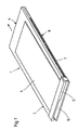
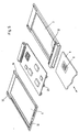
- the embodiment of the invention shown in Fig. 1 of the drawing shows a contacting unit 1 designed as a chip card reader, which is provided via a standard PCMCIA interface is contacted with a notebook become.
- the contacting unit 1 consists of a double-shell outer housing 2 with a base plate 3, a PCMCIA connector panel in the form of a Connector strip 4 with 68 poles on the in the direction of insertion into the notebook according to the arrow at the front end, an insertion guide 5 on the opposite End for the introduction of a chip card 9, for example according to ISO 78 16 and one Cover plate 6 extending parallel to and at a distance from base plate 3, which - like the base plate 3 - the connector strip 4 with the insert guide 5 rigid connects.
- the parts of the contacting unit 1 mentioned are used by those in FIG. 3 the drawing shown internal plastic profile elements made of PCB worn, which is also a PCMCIA circuit board 7 at a distance parallel to Hold the base plate 3 in such a way that an insertion channel 8 for ISO 78 16 Chip card 9 is formed, which has an insertion slot 10 of the insertion guide 5 can be inserted into the contacting unit 1.
- the chip card 9 can be in the direction of the double arrow shown in FIG.
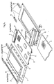
- FIG. 2 of the drawing shows the two individual shells of the outer housing, namely the base plate 3 in a perspective view of the inside and the cover plate 6, almost opened by 180 °, also in a perspective View of the inside.
- Base plate 3 and cover plate 6 are separate manageable, not interconnected sheet metal parts with inward curved Staples 12 on the long sides 13, 14 and the rear narrow side 15, while the front narrow side remains free in the direction of insertion, so that later the To be able to arrange connector strip 4.
- the embodiment is the base plate 3 with a welded Reinforcement plate 16 provided, which makes it possible to have an extremely thin Use sheet metal of approximately 2/10 mm thick.
- an amplifier plate 16 made of metal one made of plastic That can be used in a single process step with other Plastic parts described below can be produced by injection molding can.
- the staples 12 have an L-shape and it is provided that this from the Punch the sheet of the base plate 3 or cover plate 6 free by 90 ° out of the plane bend upwards and then another bend inwards by 90 ° to make so that in the later interior of the contact unit 1 protruding free leg parallel to the base plate 3 and cover plate 9 on the There is cramping, which is a particularly cheap bracket for a further Plastic molding of the staples 12 described below.
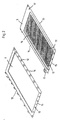
- Fig. 3 of the drawing shows a perspective view of the inner Equipping the contacting unit 1 used plastic profiles, which, however, in the preferred embodiment is not manufactured separately and in the housing are used, but in conjunction with the corresponding metal parts of the housing in a single step in the injection molding process getting produced.
- Fig. 3 of the drawing illustrates in this sense only the shape of the plastic elements. This corresponds to the breakdown of the Fig. 2 belonging to the base plate 3 plastic profile part 18, the Insert guide 5 forms, together with those belonging to base plate 3 Plastic holders 19, 20 shown on the right, during the cover plate 6 assignable U-shaped plastic frame 27 is shown on the left in the drawing.
- the assignments result more precisely from FIGS. 4 and 5 of the drawing and are described in more detail below.
- the plastic profile part 18 is made in one piece by injection molding Form of one over the entire narrow side 15 of the contacting unit 1 extending bar of substantially U-shaped cross-section, the open side of the U-shape forms the insertion slot 10, which the opposite area of the U-shape in a corresponding to the chip card 9 Width extends so that the strip-shaped forming the insertion slot 10 Upper part and the strip-shaped lower part arranged at a distance because of it of the penetrating slot are connected to one another only by webs and the insertion slot 10 of the plastic profile part 18 is open on the side.
- the Plastic profile part 18 also has one piece above the insertion slot inward platform-like extension 21, which is level with one another Holder of the circuit board 7 is provided with recesses 22, in which of the Printed circuit board 7 projecting positioning tabs 23 in assembled Intervene in the condition flush.
- the plastic holders 19 correspond to correspondingly shaped holders 25, 26 at the free ends of the U-shaped part of the cover plate 6 Plastic frame 27, the closed side only as a narrow bar 28 is formed, which with the platform-like extension 21 of the Plastic profile part 18 corresponds in the assembled state.
- the Longitudinal legs of the plastic frame 27 have an inward open guide in the form of a gradation 29 for the detection and mounting of the printed circuit board 7, which is fixed in the assembled state by the plastic frame 27, the holder 25, 26 together with the plastic holder 19, 20 of the fixation the connector strip 4 connected to the circuit board 7 serve.
- plastic elements shown in Fig. 3 of the drawing are also included various positioning projections and recesses serving for positioning 30 provided.
- the printed circuit board 7 drawn next to it is in this way on the base plate 3 arranged that the side of the connector strip 4 recognizable from the front Cam 31 in the corresponding recesses of the plastic holder 19, 20th engage and the positioning tabs 23 of the printed circuit board 7 opposite flush in the recesses 22 of the platform-like extension 21 of the Plastic profile part 18 are used.
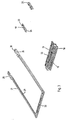
- the cover plate in FIGS. 4 and 5 of the drawing is not in the Assembly position shown, but rather opened by 180 ° to the view to allow inside. It can be seen that the cover plate 7 of the U-shaped Plastic frame 27 is assigned, which by the corresponding staples 12th is held on the cover plate 6 and for mounting on the in the described Prepared base plate 3 with circuit board 7 is placed. Come here the areas designated in the drawing as "adhesive surfaces" Plastic elements lie on top of each other and can be used to make a solid Bonded together.
- Fig. 6 of the drawing illustrates the vertical assembly of the three prefabricated Parts through the exploded view, from which it can be seen that the base plate 3rd through a single injection molding process on the inside with which the slide-in guide 5 for the chip card forming plastic profile part 18 and the two Plastic holders 19, 20 for the connector strip 4 and a plastic reinforcement plate 16 is provided.
- the base plate 3rd through a single injection molding process on the inside with which the slide-in guide 5 for the chip card forming plastic profile part 18 and the two Plastic holders 19, 20 for the connector strip 4 and a plastic reinforcement plate 16 is provided.
- the base plate 3rd through a single injection molding process on the inside with which the slide-in guide 5 for the chip card forming plastic profile part 18 and the two Plastic holders 19, 20 for the connector strip 4 and a plastic reinforcement plate 16 is provided.
- the clamps 17 are on the side and inside the Insert slot 10 are kept clear of plastic, on the one hand, a good Ensure side guidance for the chip card and on the other hand the width of the Keep contact unit
Landscapes
- Engineering & Computer Science (AREA)
- Artificial Intelligence (AREA)
- Computer Vision & Pattern Recognition (AREA)
- Physics & Mathematics (AREA)
- General Physics & Mathematics (AREA)
- Theoretical Computer Science (AREA)
- Casings For Electric Apparatus (AREA)
- Credit Cards Or The Like (AREA)
Claims (11)
- Unité (1) de mise en contact selon le standard PCMCIA, comportant une carte à circuits imprimés (7) avec des composants électroniques, qui est équipée, en supplément à une baguette de connexion par enfichage (4) agencée sur l'un des petits côtés de la carte imprimée (7), d'un champ de contacts (11') sur une surface de la carte imprimée (7) pour la mise en contact d'une carte à puce (9) qui peut être introduite parallèlement à la carte imprimée (7) à travers une fente d'introduction (10) dans un canal d'introduction (8) en forme de fente qui est ménagé entre-une plaque de base (3) et la carte imprimée (7) et qui comprend un guidage d'introduction (5) sur le petit côté (15) opposé à la baguette de connexion par enfichage (4), la carte imprimée (7) étant maintenue par un cadre (27) en matière plastique qui est agencé sur une plaque de recouvrement (6), caractérisée en ce que1.1 la plaque de base (3) et la plaque de recouvrement (6) sont des pièces en tôle séparées comprenant des crochets (12) repliés vers l'intérieur sur les grands côtés (13, 14) et/ou sur les petits côtés (15) ;1.2 la plaque de base (3) est pourvue, sur la baguette de connexion par enfichage (4) pour la saisir, d'un élément de maintien respectif (19, 20) en matière plastique du côté bordure et d'un élément profilé (18) en matière plastique en forme de baguette s'étendant sur tout le côté transversal du côté d'introduction de la carte à puce, ledit élément formant le guidage d'introduction (5) et présentant une ouverture traversante (10) en forme de fente pour la carte à puce (9) vers le canal d'introduction (8), un élargissement (21) en forme de plate-forme s'étendant vers l'intérieur étant prévu sur l'élément profilé (18) en matière plastique au-dessus de l'ouverture en fente (10) pour le maintien de la carte imprimée (7) ;1.3 sur la plaque de recouvrement (6) sont prévus une multitude de crochets (12) pour le maintien du cadre (27) en matière plastique, tandis que sur la plaque de base (3) l'élément profilé (18) en matière plastique formant le guidage d'introduction (5) est retenu par des crochets (12) sur le côté transversal (15) et par une pince respective (17) ou par un élément élastique sur chaque grand côté (13, 14), qui limitent latéralement la fente d'introduction (10) et qui forment ainsi des guidages latéraux pour la carte à puce à introduire (9) ;1.4 les éléments de maintien (19, 20) en matière plastique et l'élément profilé (18) en matière plastique sont assemblés par injection avec les crochets associés (12) de la plaque de base (3) pour former une unité composite ;1.5 la plaque de recouvrement (6) est munie, du côté intérieur, du cadre (27) en matière plastique qui est assemblé par injection avec les crochets associés (12) de la plaque de recouvrement (6), pour former une unité composite ;1.6 la plaque de recouvrement (6) et la plaque de base (3) sont reliées l'une à l'autre via les éléments en matière plastique (19, 20 ; 21, 23 ; 27) par une liaison en matière plastique, telle qu'un collage, une soudure par ultrasons ou une compression à chaud.
- Unité de mise en contact selon la revendication 1, caractérisée en ce que les éléments en matière plastique (19, 20 ; 21, 23 ; 27) de la plaque de recouvrement (6) et de la plaque de base (3) sont pourvus de saillies et d'évidements correspondants (30) ainsi que de moyens de liaison, tels que des surfaces à coller et des éléments d'orientation d'énergie (32) pour un soudage par ultrasons.
- Unité de mise en contact selon l'une ou l'autre des revendications 1 et 2, caractérisée en ce qu'il est prévu des crochets (12) en forme de L qui sont poinçonnés à partir des pièces en tôle et qui sont repliés de façon appropriée au positionnement.
- Unité de mise en contact selon l'une quelconque des revendications 1 à 3, caractérisée en ce que l'élément profilé (18) en matière plastique est d'une seule pièce et présente une section en forme de U, le côté ouvert de la forme en U formant la fente d'introduction (10) qui traverse la zone opposée de la forme en U sur une largeur qui correspond à la carte à puce (9), où l'élargissement (21) en forme de plate-forme est prévu en une seule pièce au-dessus de l'ouverture ainsi formée et est pourvu de renfoncements (22) pour le maintien à niveau égal de la carte imprimée (7), dans lesquels s'engagent en affleurement des pattes de positionnement (23) en saillie de la carte imprimée (7).
- Unité de mise en contact selon l'une quelconque des revendications 1 à 4, caractérisée en ce que les éléments de maintien (19, 20) en matière plastique de la plaque de base (3) sont réalisés sous forme de butées axiales (24) pour limiter l'introduction de la carte à puce (9).
- Unité de mise en contact selon l'une quelconque des revendications 1 à 5, caractérisée en ce que le cadre (27) en matière plastique et en forme de U est réalisé, sur son côté fermé, sous forme d'une baguette étroite qui correspond avec l'élargissement (21) en forme de plate-forme de l'élément profilé (18) en matière plastique.
- Unité de mise en contact selon la revendication 6, caractérisée en ce que les extrémités libres des bras du cadre (27) en matière plastique sont réalisées en correspondance de la réalisation des éléments de maintien (19, 20) en matière plastique de la plaque de base (3).
- Unité de mise en contact selon l'une quelconque des revendications 1 à 7, caractérisée en ce que la plaque de base (3) est renforcée du côté intérieur par une plaque de renforcement (16) en métal ou en matière plastique, le cas échéant à effet ressort, qui est collée ou soudée ou injectée en matière plastique pour former un composite.
- Procédé pour réaliser une unité de mise en contact selon l'une quelconque des revendications 1 à 8, caractérisé par les étapes suivantes :9.1 dans une première étape, on poinçonne les coques de boítier extérieures en tant que pièces en tôle à manipuler séparément non reliées l'une à l'autre, des crochets (12) et des pinces (17) étant poinçonné(e)s et replié(e)s vers l'intérieur sur la plaque de base (3) et sur la plaque de recouvrement (6) ;9.2 dans une seconde étape, on pourvoit respectivement la plaque de base (3) et la plaque de recouvrement (6) séparément d'éléments de maintien (19, 20) en matière plastique et d'un élément profilé (18) en matière plastique d'une part et du cadre (27) en matière plastique d'autre part par une opération de coulée par injection sous forme d'une unité composite ;9.3 ensuite, on pose depuis le haut la carte imprimée (7) avec sa baguette de connexion par enfichage (4) sur la plaque de base (3) et on la positionne dans l'élément profilé (18) en matière plastique et dans les éléments de maintien (19, 20) en matière plastique ;9.4 dans une étape finale, on superpose les coques de boítier ainsi prémontées avec les éléments en matière plastique (19, 20 ; 21, 23 ; 27) situés à l'intérieur et on les relie par une technique de liaison pour matière plastique, telle qu'un collage, un soudage par ultrasons ou une compression à chaud.
- Procédé selon la revendication 9, caractérisé en ce que l'on réalise l'élément profilé (18) en matière plastique formant le guidage d'introduction (5) pour la carte à puce (9) et les deux éléments de maintien (19, 20) en matière plastique pour la baguette de connexion par enfichage (4) par une seule opération de coulée par injection sur la plaque de base (3) du côté intérieur, et en ce que l'on réalise le cadre (27) en matière plastique pour la carte imprimée (7) par une autre opération de coulée par injection sur la plaque de recouvrement (6) du côté intérieur.
- Application d'une unité de mise en contact selon l'une quelconque des revendications 1 à 8 pour protéger un ordinateur portable à l'encontre d'une utilisation non autorisée, la protection pouvant être annulée par une personne autorisée au moyen de la carte à puce (9) introduite et mise en contact.
Priority Applications (5)
| Application Number | Priority Date | Filing Date | Title |
|---|---|---|---|
| DE59801853T DE59801853D1 (de) | 1998-02-20 | 1998-02-20 | Vertikal montierbarer, kurzbauender Chipkartenleser |
| EP98102950A EP0950974B1 (fr) | 1998-02-20 | 1998-02-20 | Lecteur de carte à puce compact et installable verticalement |
| DE29806656U DE29806656U1 (de) | 1998-02-20 | 1998-04-11 | Vertikal montierbarer, kurzbauender Chipkartenleser |
| JP11030891A JPH11328324A (ja) | 1998-02-20 | 1999-02-09 | チップカ―ド用接触ユニット |
| US09/253,074 US6134114A (en) | 1998-02-20 | 1999-02-19 | Vertically assembled chip card reader |
Applications Claiming Priority (1)
| Application Number | Priority Date | Filing Date | Title |
|---|---|---|---|
| EP98102950A EP0950974B1 (fr) | 1998-02-20 | 1998-02-20 | Lecteur de carte à puce compact et installable verticalement |
Publications (2)
| Publication Number | Publication Date |
|---|---|
| EP0950974A1 EP0950974A1 (fr) | 1999-10-20 |
| EP0950974B1 true EP0950974B1 (fr) | 2001-10-24 |
Family
ID=8231452
Family Applications (1)
| Application Number | Title | Priority Date | Filing Date |
|---|---|---|---|
| EP98102950A Expired - Lifetime EP0950974B1 (fr) | 1998-02-20 | 1998-02-20 | Lecteur de carte à puce compact et installable verticalement |
Country Status (4)
| Country | Link |
|---|---|
| US (1) | US6134114A (fr) |
| EP (1) | EP0950974B1 (fr) |
| JP (1) | JPH11328324A (fr) |
| DE (2) | DE59801853D1 (fr) |
Families Citing this family (49)
| Publication number | Priority date | Publication date | Assignee | Title |
|---|---|---|---|---|
| US6460772B1 (en) * | 1998-09-01 | 2002-10-08 | Intertex Data Ab | PCMCIA smart card reader |
| US6293464B1 (en) * | 1999-01-05 | 2001-09-25 | Jared Joseph Smalley, Jr. | Card reader |
| DE29900768U1 (de) * | 1999-01-18 | 2000-03-02 | Siemens AG, 80333 München | Einrichtung zum Anschluß eines Bussystems an eine Recheneinheit, eine Steckkarte für eine Schnittstelle nach Art des PCMCIA-Standards sowie ein Adapter für eine derartige Einrichtung |
| US6371376B1 (en) * | 1999-04-16 | 2002-04-16 | Ho J. Dan | PCMCIA card with secure smart card reader |
| FR2800923A1 (fr) * | 1999-11-08 | 2001-05-11 | Framatome Connectors Int | Lecteur de carte a micro-circuit |
| US6392257B1 (en) | 2000-02-10 | 2002-05-21 | Motorola Inc. | Semiconductor structure, semiconductor device, communicating device, integrated circuit, and process for fabricating the same |
| US6693033B2 (en) | 2000-02-10 | 2004-02-17 | Motorola, Inc. | Method of removing an amorphous oxide from a monocrystalline surface |
| JP2001332872A (ja) * | 2000-05-19 | 2001-11-30 | Matsushita Electric Ind Co Ltd | 携帯端末装置 |
| KR20030011083A (ko) | 2000-05-31 | 2003-02-06 | 모토로라 인코포레이티드 | 반도체 디바이스 및 이를 제조하기 위한 방법 |
| US7295443B2 (en) | 2000-07-06 | 2007-11-13 | Onspec Electronic, Inc. | Smartconnect universal flash media card adapters |
| US6438638B1 (en) | 2000-07-06 | 2002-08-20 | Onspec Electronic, Inc. | Flashtoaster for reading several types of flash-memory cards with or without a PC |
| WO2002009187A2 (fr) | 2000-07-24 | 2002-01-31 | Motorola, Inc. | Diodes a heterojonction tunnel et processus de fabrication de celles-ci |
| US6555946B1 (en) | 2000-07-24 | 2003-04-29 | Motorola, Inc. | Acoustic wave device and process for forming the same |
| US6638838B1 (en) | 2000-10-02 | 2003-10-28 | Motorola, Inc. | Semiconductor structure including a partially annealed layer and method of forming the same |
| US20020096683A1 (en) | 2001-01-19 | 2002-07-25 | Motorola, Inc. | Structure and method for fabricating GaN devices utilizing the formation of a compliant substrate |
| US6673646B2 (en) | 2001-02-28 | 2004-01-06 | Motorola, Inc. | Growth of compound semiconductor structures on patterned oxide films and process for fabricating same |
| WO2002082551A1 (fr) | 2001-04-02 | 2002-10-17 | Motorola, Inc. | Structure de semi-conducteur a courant de fuite attenue |
| US6709989B2 (en) | 2001-06-21 | 2004-03-23 | Motorola, Inc. | Method for fabricating a semiconductor structure including a metal oxide interface with silicon |
| US6992321B2 (en) | 2001-07-13 | 2006-01-31 | Motorola, Inc. | Structure and method for fabricating semiconductor structures and devices utilizing piezoelectric materials |
| US6646293B2 (en) | 2001-07-18 | 2003-11-11 | Motorola, Inc. | Structure for fabricating high electron mobility transistors utilizing the formation of complaint substrates |
| US7019332B2 (en) | 2001-07-20 | 2006-03-28 | Freescale Semiconductor, Inc. | Fabrication of a wavelength locker within a semiconductor structure |
| US6693298B2 (en) | 2001-07-20 | 2004-02-17 | Motorola, Inc. | Structure and method for fabricating epitaxial semiconductor on insulator (SOI) structures and devices utilizing the formation of a compliant substrate for materials used to form same |
| US6855992B2 (en) | 2001-07-24 | 2005-02-15 | Motorola Inc. | Structure and method for fabricating configurable transistor devices utilizing the formation of a compliant substrate for materials used to form the same |
| US6667196B2 (en) | 2001-07-25 | 2003-12-23 | Motorola, Inc. | Method for real-time monitoring and controlling perovskite oxide film growth and semiconductor structure formed using the method |
| US6639249B2 (en) | 2001-08-06 | 2003-10-28 | Motorola, Inc. | Structure and method for fabrication for a solid-state lighting device |
| US6589856B2 (en) | 2001-08-06 | 2003-07-08 | Motorola, Inc. | Method and apparatus for controlling anti-phase domains in semiconductor structures and devices |
| US20030034491A1 (en) | 2001-08-14 | 2003-02-20 | Motorola, Inc. | Structure and method for fabricating semiconductor structures and devices for detecting an object |
| US6673667B2 (en) | 2001-08-15 | 2004-01-06 | Motorola, Inc. | Method for manufacturing a substantially integral monolithic apparatus including a plurality of semiconductor materials |
| US6783926B2 (en) * | 2001-09-15 | 2004-08-31 | Kenneth Reece | Circuit board IC card connector |
| US20030071327A1 (en) | 2001-10-17 | 2003-04-17 | Motorola, Inc. | Method and apparatus utilizing monocrystalline insulator |
| US6916717B2 (en) | 2002-05-03 | 2005-07-12 | Motorola, Inc. | Method for growing a monocrystalline oxide layer and for fabricating a semiconductor device on a monocrystalline substrate |
| US6786415B2 (en) * | 2002-08-06 | 2004-09-07 | Jung-Hua Yiu | Memory card connector |
| US6915956B2 (en) * | 2002-08-12 | 2005-07-12 | Carry Computer Eng. Co., Ltd. | Universal flash memory card bank structure |
| US7169619B2 (en) | 2002-11-19 | 2007-01-30 | Freescale Semiconductor, Inc. | Method for fabricating semiconductor structures on vicinal substrates using a low temperature, low pressure, alkaline earth metal-rich process |
| US6885065B2 (en) | 2002-11-20 | 2005-04-26 | Freescale Semiconductor, Inc. | Ferromagnetic semiconductor structure and method for forming the same |
| US7020374B2 (en) | 2003-02-03 | 2006-03-28 | Freescale Semiconductor, Inc. | Optical waveguide structure and method for fabricating the same |
| US6965128B2 (en) | 2003-02-03 | 2005-11-15 | Freescale Semiconductor, Inc. | Structure and method for fabricating semiconductor microresonator devices |
| US7044380B2 (en) * | 2003-08-22 | 2006-05-16 | International Business Machines Corporation | Methods, systems and computer program products for communicating product status information |
| DE20319145U1 (de) * | 2003-12-10 | 2004-02-19 | Stocko Contact Gmbh & Co. Kg | Kontaktiereinheit |
| GB0404922D0 (en) * | 2004-03-04 | 2004-04-07 | Dione Plc | Secure card reader |
| US7177159B2 (en) * | 2004-05-03 | 2007-02-13 | 3 View Technology Co., Ltd. | Packaging structure of electronic card |
| US6929487B1 (en) * | 2004-09-02 | 2005-08-16 | Yazaki North America, Inc. | Terminal block arrangement for a printed circuit board in a smart connector |
| FR2887357A1 (fr) * | 2005-06-20 | 2006-12-22 | Gemplus Sa | Procede de fabrication d'un objet electronique comportant une etape de transfert de donnees et objet obtenu |
| US7500611B2 (en) * | 2006-09-20 | 2009-03-10 | Tyco Electronics Corporation | Vertical mount smart card reader assembly |
| KR100790403B1 (ko) | 2007-03-16 | 2008-01-03 | (주)우전 | 개인용컴퓨터 등의 확장형 카드패키지 및 그 제조방법 |
| US20090196006A1 (en) * | 2008-02-04 | 2009-08-06 | Yi-Chen Chen | Substrate structure of secure digital input/output module interface and its manufacturing method |
| ITTS20080003A1 (it) * | 2008-02-14 | 2009-08-15 | Telit Communications Spa | Modulo di connettivita' da macchina a macchina ad elevata versatilita' |
| WO2010099305A2 (fr) * | 2009-02-27 | 2010-09-02 | Dualsonic, Llc | Boîtier électronique, ensembles pour celui-ci et ses procédés de fabrication |
| CN105101631B (zh) * | 2015-08-12 | 2017-11-28 | 深圳市兴森快捷电路科技股份有限公司 | 一种用于辅助pcb板对接的固定装置 |
Family Cites Families (11)
| Publication number | Priority date | Publication date | Assignee | Title |
|---|---|---|---|---|
| FR2686172B1 (fr) * | 1992-01-14 | 1996-09-06 | Gemplus Card Int | Carte enfichable pour microordinateur formant lecteur de carte a contacts affleurants. |
| US5397857A (en) * | 1993-07-15 | 1995-03-14 | Dual Systems | PCMCIA standard memory card frame |
| JP3559319B2 (ja) * | 1994-09-29 | 2004-09-02 | 株式会社東芝 | Icカード情報処理装置 |
| US5475919B1 (en) * | 1994-10-07 | 2000-10-17 | Three View Technology Co Ltd | Pcmcia card manufacturing process |
| TW310872U (en) | 1995-09-22 | 1997-07-11 | View Technology Co Ltd 3 | Improved structure of housing cover for PCMCIA card |
| EP0891633A4 (fr) * | 1996-04-05 | 2000-12-06 | Berg Electronics Mfg | Carte memoire pcmcia |
| DE29607253U1 (de) * | 1996-04-22 | 1996-07-04 | Stocko Metallwarenfabriken Henkels & Sohn GmbH & Co, 42327 Wuppertal | Kombichipkartenleser |
| US5752857A (en) * | 1996-05-24 | 1998-05-19 | Itt Corporation | Smart card computer adaptor |
| DE29615553U1 (de) * | 1996-09-06 | 1996-10-31 | Stocko Metallwarenfabriken Henkels Und Sohn Gmbh & Co, 42327 Wuppertal | Gehäuse für Personal-Computer-Karten (PC-Cards) |
| US5969330A (en) * | 1996-11-20 | 1999-10-19 | The Whitaker Corporation | Smart card reader with hinged cover and cover actuating surface |
| US5936222A (en) * | 1997-10-03 | 1999-08-10 | The Whitaker Corporation | Smart card reader having pivoting contacts |
-
1998
- 1998-02-20 DE DE59801853T patent/DE59801853D1/de not_active Expired - Fee Related
- 1998-02-20 EP EP98102950A patent/EP0950974B1/fr not_active Expired - Lifetime
- 1998-04-11 DE DE29806656U patent/DE29806656U1/de not_active Expired - Lifetime
-
1999
- 1999-02-09 JP JP11030891A patent/JPH11328324A/ja active Pending
- 1999-02-19 US US09/253,074 patent/US6134114A/en not_active Expired - Fee Related
Also Published As
| Publication number | Publication date |
|---|---|
| JPH11328324A (ja) | 1999-11-30 |
| DE29806656U1 (de) | 1998-07-30 |
| DE59801853D1 (de) | 2001-11-29 |
| EP0950974A1 (fr) | 1999-10-20 |
| US6134114A (en) | 2000-10-17 |
Similar Documents
| Publication | Publication Date | Title |
|---|---|---|
| EP0950974B1 (fr) | Lecteur de carte à puce compact et installable verticalement | |
| EP1008280B1 (fr) | Unite de mise en contact pour un element de support en forme de carte de modules electroniques, en particulier correspondant a la norme pcmcia | |
| EP2481935B1 (fr) | Procédé de montage d'un composant et clip de fixation | |
| EP0924640B1 (fr) | Adaptateur pour le contact de cartes à puce | |
| EP1418528B1 (fr) | Lecteur de carte à puce | |
| DE4406644C2 (de) | Steckkarte für elektronische Datenverarbeitungsgeräte und Verfahren zu dessen Herstellung und Montage | |
| DE69508569T2 (de) | Sekundär anschluss verriegelungs element | |
| DE3810274C2 (de) | Chipkarten-Kontaktiergerät | |
| DE29909222U1 (de) | PC-Card Chipkartenleser | |
| DE102019104559A1 (de) | Halterahmen für eine Steckverbinder | |
| DE29617034U1 (de) | PC-Card Adapter | |
| DE29819389U1 (de) | Chipkarte | |
| EP0976082B1 (fr) | Dispositif d'interface pour cartes a puce | |
| DE69803549T2 (de) | Kartenleseverbindung | |
| EP2401790B1 (fr) | Connexion électrique à souder | |
| DE202010004995U1 (de) | Befestiger zur Befestigung eines ersten Bauteils an einem zweiten Bauteil | |
| EP1924946B1 (fr) | Connecteur de carte intelligente comportant un dispositif de protection conçu pour des cartes a faible espacement | |
| DE20018740U1 (de) | Gehäuse für Telekommunikationsanlagen | |
| BE1031455B1 (de) | Halterahmen für einen Steckverbinder | |
| DE29723227U1 (de) | Schnittstellen-Vorrichtung für Chipkarten | |
| DE102004032104B4 (de) | Kontaktiereinheit zum Lesen und/oder Beschreiben von Chipkarten | |
| DE102004011601B4 (de) | Trägerplatte mit einer Kontaktfeder für Antennenverstärker | |
| DE20210362U1 (de) | PC-Card Chipkartenleser | |
| WO2005057470A1 (fr) | Unite de contact | |
| DE102023107157A1 (de) | Halterahmen für einen Steckverbinder |
Legal Events
| Date | Code | Title | Description |
|---|---|---|---|
| PUAI | Public reference made under article 153(3) epc to a published international application that has entered the european phase |
Free format text: ORIGINAL CODE: 0009012 |
|
| 17P | Request for examination filed |
Effective date: 19980922 |
|
| AK | Designated contracting states |
Kind code of ref document: A1 Designated state(s): DE FR GB IT |
|
| AX | Request for extension of the european patent |
Free format text: AL;LT;LV;MK;RO;SI |
|
| AKX | Designation fees paid |
Free format text: DE FR GB IT |
|
| 17Q | First examination report despatched |
Effective date: 20000529 |
|
| GRAG | Despatch of communication of intention to grant |
Free format text: ORIGINAL CODE: EPIDOS AGRA |
|
| GRAG | Despatch of communication of intention to grant |
Free format text: ORIGINAL CODE: EPIDOS AGRA |
|
| GRAH | Despatch of communication of intention to grant a patent |
Free format text: ORIGINAL CODE: EPIDOS IGRA |
|
| RAP1 | Party data changed (applicant data changed or rights of an application transferred) |
Owner name: STOCKO CONTACT GMBH & CO. KG |
|
| GRAH | Despatch of communication of intention to grant a patent |
Free format text: ORIGINAL CODE: EPIDOS IGRA |
|
| GRAA | (expected) grant |
Free format text: ORIGINAL CODE: 0009210 |
|
| AK | Designated contracting states |
Kind code of ref document: B1 Designated state(s): DE FR GB IT |
|
| REF | Corresponds to: |
Ref document number: 59801853 Country of ref document: DE Date of ref document: 20011129 |
|
| GBT | Gb: translation of ep patent filed (gb section 77(6)(a)/1977) |
Effective date: 20011108 |
|
| ET | Fr: translation filed | ||
| REG | Reference to a national code |
Ref country code: GB Ref legal event code: IF02 |
|
| PLBE | No opposition filed within time limit |
Free format text: ORIGINAL CODE: 0009261 |
|
| STAA | Information on the status of an ep patent application or granted ep patent |
Free format text: STATUS: NO OPPOSITION FILED WITHIN TIME LIMIT |
|
| 26N | No opposition filed | ||
| PGFP | Annual fee paid to national office [announced via postgrant information from national office to epo] |
Ref country code: GB Payment date: 20040130 Year of fee payment: 7 |
|
| PGFP | Annual fee paid to national office [announced via postgrant information from national office to epo] |
Ref country code: FR Payment date: 20040209 Year of fee payment: 7 |
|
| PGFP | Annual fee paid to national office [announced via postgrant information from national office to epo] |
Ref country code: DE Payment date: 20040419 Year of fee payment: 7 |
|
| PG25 | Lapsed in a contracting state [announced via postgrant information from national office to epo] |
Ref country code: IT Free format text: LAPSE BECAUSE OF NON-PAYMENT OF DUE FEES Effective date: 20050220 Ref country code: GB Free format text: LAPSE BECAUSE OF NON-PAYMENT OF DUE FEES Effective date: 20050220 |
|
| PG25 | Lapsed in a contracting state [announced via postgrant information from national office to epo] |
Ref country code: DE Free format text: LAPSE BECAUSE OF NON-PAYMENT OF DUE FEES Effective date: 20050901 |
|
| GBPC | Gb: european patent ceased through non-payment of renewal fee |
Effective date: 20050220 |
|
| PG25 | Lapsed in a contracting state [announced via postgrant information from national office to epo] |
Ref country code: FR Free format text: LAPSE BECAUSE OF NON-PAYMENT OF DUE FEES Effective date: 20051031 |
|
| REG | Reference to a national code |
Ref country code: FR Ref legal event code: ST Effective date: 20051031 |