EP0952442A2 - Appareil et procédé d'inspection visuelle - Google Patents
Appareil et procédé d'inspection visuelle Download PDFInfo
- Publication number
- EP0952442A2 EP0952442A2 EP99108015A EP99108015A EP0952442A2 EP 0952442 A2 EP0952442 A2 EP 0952442A2 EP 99108015 A EP99108015 A EP 99108015A EP 99108015 A EP99108015 A EP 99108015A EP 0952442 A2 EP0952442 A2 EP 0952442A2
- Authority
- EP
- European Patent Office
- Prior art keywords
- image
- areas
- defective
- pair
- frame
- Prior art date
- Legal status (The legal status is an assumption and is not a legal conclusion. Google has not performed a legal analysis and makes no representation as to the accuracy of the status listed.)
- Withdrawn
Links
- 238000011179 visual inspection Methods 0.000 title claims description 21
- 238000000034 method Methods 0.000 title claims description 12
- 230000002950 deficient Effects 0.000 claims abstract description 70
- 238000003384 imaging method Methods 0.000 claims description 7
- 238000007689 inspection Methods 0.000 abstract description 3
- 239000004065 semiconductor Substances 0.000 abstract description 3
- 230000007547 defect Effects 0.000 description 34
- 238000001514 detection method Methods 0.000 description 7
- 238000010586 diagram Methods 0.000 description 2
- 239000004973 liquid crystal related substance Substances 0.000 description 2
- 238000010276 construction Methods 0.000 description 1
- 238000007796 conventional method Methods 0.000 description 1
- 238000013500 data storage Methods 0.000 description 1
- 230000010354 integration Effects 0.000 description 1
- 238000012986 modification Methods 0.000 description 1
- 230000004048 modification Effects 0.000 description 1
- 230000003287 optical effect Effects 0.000 description 1
- 230000035945 sensitivity Effects 0.000 description 1
Images


Classifications
-
- G—PHYSICS
- G01—MEASURING; TESTING
- G01B—MEASURING LENGTH, THICKNESS OR SIMILAR LINEAR DIMENSIONS; MEASURING ANGLES; MEASURING AREAS; MEASURING IRREGULARITIES OF SURFACES OR CONTOURS
- G01B11/00—Measuring arrangements characterised by the use of optical techniques
- G01B11/30—Measuring arrangements characterised by the use of optical techniques for measuring roughness or irregularity of surfaces
-
- G—PHYSICS
- G01—MEASURING; TESTING
- G01N—INVESTIGATING OR ANALYSING MATERIALS BY DETERMINING THEIR CHEMICAL OR PHYSICAL PROPERTIES
- G01N21/00—Investigating or analysing materials by the use of optical means, i.e. using sub-millimetre waves, infrared, visible or ultraviolet light
- G01N21/84—Systems specially adapted for particular applications
- G01N21/88—Investigating the presence of flaws or contamination
- G01N21/95—Investigating the presence of flaws or contamination characterised by the material or shape of the object to be examined
- G01N21/956—Inspecting patterns on the surface of objects
- G01N21/95607—Inspecting patterns on the surface of objects using a comparative method
-
- G—PHYSICS
- G01—MEASURING; TESTING
- G01N—INVESTIGATING OR ANALYSING MATERIALS BY DETERMINING THEIR CHEMICAL OR PHYSICAL PROPERTIES
- G01N21/00—Investigating or analysing materials by the use of optical means, i.e. using sub-millimetre waves, infrared, visible or ultraviolet light
- G01N21/84—Systems specially adapted for particular applications
- G01N21/88—Investigating the presence of flaws or contamination
- G01N21/95—Investigating the presence of flaws or contamination characterised by the material or shape of the object to be examined
- G01N21/9501—Semiconductor wafers
Definitions
- the present invention relates generally to a visual inspection apparatus and method, and more particularly to a visual inspection apparatus and method applied to find defects in patterns on a semiconductor wafer, a photo mask, a liquid crystal display, or the like.
- an image obtaining part which is composed of an optical microscope and an imaging device such as a time delay and integration (TDI) sensor, obtains images of the patterns represented with multiple values while continuously scanning the object along the x-axis.
- the obtained images are stored in an image data storage part such as a memory.
- each chip is compared with two adjacent chips regardless of whether the chip has a possibility of being defective or not. Therefore, an image comparison part must have the adequate capacity for this purpose, which requires a higher cost.
- edge chips Only the single detection is performed for edge chips. Thus, the unreliable inspection must be allowed, only the edge chips are not determined, or, only the area that is determined as having a possibility of being defective as a result of the single detection is scanned again after the inspection with respect to the entire surface of the wafer, and the edge chip is compared with the second chip from the edge chip to thereby determine whether the edge chip has a possibility of being defective.
- the last chip in each scanning line is compared with the first chip in the next scanning line in the double detection. Since, however, the straightness in the scanning direction along the x-axis is higher than the absolute position accuracy along the y-axis, the difference of the images along the y-axis is greater than that of the images of chips in the same scanning lines. Consequently, the images are badly deteriorated by the sub-pixel alignment during the comparison of the images.
- the present invention is directed to a visual inspection apparatus, comprising: an imaging means for obtaining images of a plurality of areas on an object; a first image comparison means for designating the plurality of areas in pairs and comparing the images of the areas in each of the pairs to determine whether said each of the pairs is a defective pair including a defective area containing a defective part; and a second image comparison means for comparing the image of one of the areas in the pair determined as the defective pair by the first image comparison means with the image of one of the areas in another of the pairs to determine whether the one of the areas in the pair determined as the defective pair is the defective area.
- the first image comparison means may designate the plurality of areas in the pairs of two areas adjacent to one another.
- the second image comparison means may compare the image of the one of the areas in the pair determined as the defective pair with the image of one of the areas in another of the pairs adjacent to the one of the areas in the pair determined as the defective pair.
- the second image comparison means may compare only a suspected part, including a possible defective part determined by the first image comparison means, of the image of the one of the areas in the pair determined as the defective pair with a part, corresponding to the suspected part, of the image of the one of the areas in said another of the pairs.
- the images of all areas on the object are not always compared twice.
- the areas are paired, and two images are compared in each pair. Only an image in the pair, which is possibly defective, is compared with an image in another pair. This reduces the number of comparisons to almost fifty percent of that of the prior art and increases the processing speed while maintaining the reliability of the conventional double detection.
- Fig. 1 is a view showing the entire structure of a preferred embodiment of a visual inspection apparatus, which determines whether each chip on a wafer contains a defective part or not.
- the visual inspection apparatus comprises: a control part 12, which performs a variety of processing; an XY stage 14, which moves along X and Y axes horizontally under the control of the control part 12; a sample table 16 provided on the XY stage 14; a microscope 18 arranged above the sample table 16; and a TDI sensor 20 attached at the focusing position of the microscope 18.
- a wafer W as an object is placed on the sample table 16.
- An image of the surface of the wafer W is enlarged and formed on an imaging surface of the TDI sensor 20 by the microscope 18.
- the TDI sensor 20 is a multistage sensor composed of one-dimensional line sensors such as charge-coupled device (CCD) line sensors. Signal electric charges accumulated in CCD elements of the line sensor at each stage are sequentially transferred to CCD elements of the line sensor at the next stage in synchronism with a scanning speed. Consequently, a plurality of CCD elements overlaps the signal electric charges at one point subject for imaging. Therefore, even if the electric charges are accumulated in each CCD element only for a short period, the signal electric charges at each point subject for imaging are amplified to make up for the shortage in the quantity of light. Thus, the TDI sensor 20 is able to scan the images at a higher speed than the ordinary single-stage CCD line sensor.
- CCD charge-coupled device
- the TDI sensor 20 scans the surface of the wafer W along the X-axis.
- the TDI sensor 20 scans the surface image of the wafer W, which is moved by the XY stage 14 along the X-axis.
- the TDI sensor 20 is used as the imaging means, but it is possible to use the ordinary one-dimensional sensor such as the CCD line sensor or a two-dimensional sensor.
- the control part 12 controls the XY stage 14 to move the wafer W along the X and Y-axes.
- the control part 12 controls the TDI sensor 20, which relatively scans the wafer W, and obtains the surface image of the wafer W from the TDI sensor 20.
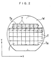
- Fig. 2 shows an example of a scanning track of the TDI sensor 20 on the wafer W under the control of the control part 12. As shown in Fig. 2, a number of chips T are regularly arranged along the X and Y-axes on the wafer W, and the chips have the same patterns. As indicated by a dashed and dotted line in Fig.
- the TDI sensor 20 starts scanning the wafer W along the X-axis from the upper left corner of a chip T s on the highest line, and reciprocally scans the wafer W until it reaches a chip T e on the lowest line.
- the TDI sensor 20 shifts the scanning line along the Y-axis downward little by little (by the image reading width (scanning width) in a direction along the Y-axis perpendicular to the scanning direction along the X-axis) to complete the scanning for all the chips T arranged on the wafer W.
- the scanning is not necessarily performed on the scanning track in Fig. 2, but the scanning may also be performed in any other scanning tracks.
- control part 12 sends the obtained surface image of the wafer W to a defect detecting part, which is a component of the control part 12.
- the defect detecting part detects a defective part in each chip on the wafer W.
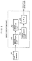
- Fig. 3 is a block diagram showing an embodiment of the defect detecting part in the control part 12.
- the defect detecting part comprises a signal processing part 50, an image storage part 52, an image comparison part 54, and a CPU 56.
- the signal processing part 50 receives image signals sequentially from the TDI sensor 20, and converts the image signals into digital image data.
- the signal processing part 50 outputs the image data to the image storage part 52.
- the image storage part 52 is composed of a memory such as a RAM.
- the image data which is output from the signal processing part 50, is sequentially stored in the image storage part 52.
- the image comparison part 54 reads the image data sequentially from the image storage part 52, and compares the image data of a pair of chips that are adjacent to one another along the X-axis to detect the defective part in the chips.
- the image comparison part 54 sends the results to the CPU 56.
- the CPU 56 compares the image data of a possible defective chip determined by the image comparison part 54 with image data of a chip different from the chip with which the possible defective chip has been compared, so as to determine whether the possible defective chip is really defective or not.
- the CPU 56 finds defective chips in this way and outputs the results to a monitor, etc.
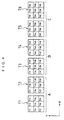
- the width of each frame along the Y-axis is the scanning width of the TDI sensor 20, and the width of each frame along the X-axis is predetermined arbitrarily.
- one chip is divided into nine frames (3 ⁇ 3 frames) to simplify the description in Figs. 4 and 5, the number of divided frames actually varies according to the size of the chip, the scanning width of the TDI sensor 20, etc.
- the scanning starts at a frame t 11 on the first line of the chip T1 in the case that the TDI sensor 20 scans the wafer W on the scanning track in Fig.2, the image data of the frames on the first line of the chips T1-T6 are sequentially recorded in the image storage part 52, and the image data of the frames on the second line of the chips T6-T1 are sequentially recorded in the image storage part 52. Then, the image data of the frames on the third line of the chips T1-T6 are sequentially recorded in the image storage part 52.
- the image comparison part 54 designates the chips T1-T6 arranged along the X-axis in pairs of two adjacent chips in such a way that one chip does not belong to two pairs or more.
- the chips T1 and T2 are paired as A; the chips T3 and T4 are paired as B; and the chips T5 and T6 are paired as C.
- a pair of frames at the same position in the two chips (the frames t mn with the same value of n ) in each pair A-C are compared.
- the image comparison part 54 reads the image data of two frames subjected to comparison from the image storage part 52.
- the image comparison part 54 compares the image data and detects a defective part in those frames. Then, the image comparison part 54 reads the image data of another two frames subjected to the next comparison from the image storage part 52 to perform the same processing.
- the image comparison part 54 finds difference between image data of the frames t 31 and t 41 with respect to each pixel. Then, the image comparison part 54 calculates the difference image data D in which value of each pixel is the difference.
- all the pixels of the difference image data D represent smaller values than a predetermined threshold. If there is at least one defective part in at least one of the frames t 31 and t 41 , a defective pixel corresponding to the defective part represents a larger value than the threshold.
- the threshold is determined according to the sensitivity for detecting the defective part.
- the image comparison part 54 After calculating the difference image data D, the image comparison part 54 compares the value of each pixel in the difference image data D with the threshold. If the values of all the pixels are equal to or less than the threshold, the image comparison part 54 determines that there is no defective part in the frames t 31 and t 41 . The image comparison part 54 sends the determination results to the CPU 56.
- the image comparison part 54 determines that there is at least one defective part in the frame t 31 and/or t 41 and sends the determination results to the CPU 56.
- the determination results include the data indicating the position of the defective pixel as well as the data indicating the presence of the defect.
- the CPU 56 compares the image data of only the frames in the possible defective pair that have been determined as being possibly defective by the image comparison part 54, with the image data of the frames in another pair. With respect to the frames that have been determined as being not defective, the CPU 56 only receives the results from the image comparison part 54 and does not perform any processing that will be described below for the frames. This reduces the processing time of the CPU 56, and eliminates the necessity of employing a CPU with a high processing capability in the visual inspection apparatus of the present invention.
- the CPU 56 reads image data of the frame t 31 in the chip T3 and image data of a frame t 21 of the chip T2 in the pair A adjacent to the chip T3 from the image storage part 52. At this time, the CPU 56 does not read all the image data of the frames t 31 and t 21 , but reads only the image data within a predetermined suspected part d including the defective pixel, which has been determined in the difference image data D. Incidentally, all the image data of the frames may be read.
- the CPU 56 calculates difference image data E1 of the image data of the frames t 31 and t 21 within the suspected part d in the same manner as the image comparison part 54, and compares a value of each pixel in the difference image data E1 with the threshold. If a larger value than the threshold is detected, the CPU 56 determines that there is a defective part in the frame t 31 of the chip T3, and outputs the determination results indicating the presence of the defective part in the chip T3 to the monitor.
- the CPU 56 determines that there is no defective part in the frame t 31 of the chip T3. Then, the CPU 56 calculates difference image data E2 of the image data of the frames t 41 of the chip T4 and a frame t 51 of the chip T5 in the pair C adjacent to the chip T4, and compares a value of each pixel in the difference image data E2 with the threshold. If a larger value than the threshold is detected, the CPU 56 determines that there is a defective part in the frame t 41 of the chip T4 and outputs the determination results indicating the presence of the defect in the chip T4 to the monitor. If all the values in the difference image data E2 are equal to or less than the threshold, the CPU 56 determines that there is no defective part in the frame t 41 of the chip T4.
- Fig. 6 is a flow chart generalizing the procedure of the image comparison part 54 and the CPU 56 for comparing the image data of the frames and detecting defective parts.
- the frame at the certain position of an n -th chip from the left is referred to as an n -th frame.
- the ( n -1)-th frame and the ( n + 1)-th frame are at the same position as the n -th frame in chips adjacent to the chip including the n - th frame.
- the total number of the chips along the X-axis is 2 N ( N is an integral number), and the first frame through the 2 N -th frame are at the same position of the chips.
- the image comparison part 54 sets the variable n as 1 (S10), and reads the image data of the (2 n - 1)-th frame and the 2 n -th frame from the image storage part 52 and compares the image data between these two frames (S12). Specifically, the first frame and the second frame are subjected to the comparison. Then, the image comparison part 54 determines whether there is any defect or not in these frames (S14). If the image comparison part 54 determines that there is no defect, it determines whether the variable n is equal to N or not, specifically whether the 2 n -th frame is the last frame or not (S16).
- the image comparison part 54 increases the variable n by 1 (S18) and reads the image data of the next two frames subjected to comparison (the third frame and the fourth frame) from the image storage part 52. Then, the image comparison part 54 compares the image data between the third and fourth frames. If no defect is detected from the frames and the variable n is determined as being equal to N at S16, the image comparison part 54 finishes the comparison and determination.
- the CPU 56 determines whether the (2 n - 1)-th frame is located in the chip at the left end (S20). In other words, the CPU 56 determines whether (2 n - 1) is equal to 1 or not. If the (2 n - 1)-th frame is not located in the chip at the left end, the CPU 56 reads the image data of the (2 n - 1)-th frame and the adjacent (2 n - 2)-th frame from the image storage part 52. Then, the CPU 56 compares the image data between the (2 n - 1)-th frame and the (2 n - 2)-th frame (S22). The suspected part for reading the image data has already been described.
- the CPU 56 reads the image data of the (2 n - 1)-th frame and the (2 n + 1)-th frame (the third frame) from the image storage part 52.
- the CPU 56 compares the image data between the (2 n - 1)-th frame and the (2 n + 1)-th frame (S24).
- the CPU 56 determines whether there is any defect in the frames (S26). If there is a defect, the CPU 56 determines that there is a defect in the (2 n - 1)-th frame (S28) and determines that there is a defect in the chip including the (2 n - 1)-th frame. On the other hand, if there is no defect, the CPU 56 determines that there is no defect in the (2 n - 1)-th frame (S30).
- the CPU 56 also performs the comparison and determination for the 2 n -th frame in the same manner as in the comparison and determination for the (2 n - 1)-th frame.
- the CPU 56 determines whether the 2 n -th frame is located in the chip at the right end (S32). In other words, the CPU 56 determines whether 2 n is N or not. If the 2 n -th frame is not located in the chip at the right end, the CPU 56 reads the image data of the 2 n -th frame and the (2 n + 1)-th frame adjacent to the 2 n -th frame from the image storage part 52 and compare the image data between the 2 n -th frame and the (2 n + 1)-th frame (S34).
- the CPU 56 reads the image data of the 2 n -th frame and the (2 n - 2)-th frame (the (2 N - 2)-th frame), which is the second frame to the left from the 2 n -th frame, from the image storage part 52. Then, the CPU 56 compares the image data between the 2 n -th frame and the (2 n - 2)-th frame (S36).
- the CPU 56 determines whether there is any defect or not in the frames (S38). If there is any defect, the CPU 56 determines that there is a defect in the 2 n -th frame (S40) and determines that there is a defect in the chip including the 2 n -th frame. On the other hand, if there is no defect, the CPU 56 determines that there is no defect in the 2 n -th frame (S42).
- the CPU 56 determines whether the variable n is equal to N or not (S16). If the variable n is not equal to N , the CPU 56 increases the variable n by 1 (S18) and repeats the processing from S12. If the variable n is equal to N at S16, the CPU 56 finishes the comparison and determination. Thus, the determination about the presence of the defect is completed for the frames at the corresponding positions in all the chips arranged along the X-axis.
- the image comparison part 54 does not always perform the comparison and determination twice for all the frames.
- the image comparison part 54 performs the comparison and determination once for all the frames, and then the CPU 56 performs the comparison and determination only for the suspected frame, which has been determined as being possibly defective by the image comparison part 54. This reduces the processing of the defect detecting part to almost fifty percent of that of the prior art, and increases the processing speed.
- the total number of the chips arranged along the X-axis is an even number. Thus, no chip is left over when the chips are designated in the pairs as shown in Fig. 4. If, however, the total number of chips is an odd number, one chip is left over. In this case, one of the other chips is duplicatively paired with the leftover chip so that the defect in the leftover chip can be detected in the above-described comparison and determination procedure.
- the image comparison part 54 compares the image data in a pair of adjacent chips, but the adjacent chips are not necessarily paired. Comparing the image data in a pair of separate chips also reduces the processing and increases the processing speed.
- the comparison of the image data and the determination about the presence of the defect may be sequentially performed while the TDI sensor 20 is obtaining the image data or after the image data of all the chips are obtained. If the comparison and determination are sequentially performed while the TDI sensor 20 is obtaining the image data, it is possible to use a memory with a small capacity that can store the image data of at least three frames as the image storage part 52. This reduces the cost of the memory.
- the present invention is applied to the visual inspection apparatus for inspecting the wafer on which the chips with the same pattern are arranged, but the present invention may also be applied to a visual inspection apparatus for inspecting an arbitrary object other than the wafer.
- the images in all areas on the object are not always compared twice. Two areas are paired and the images are compared in each pair. Only the images in the suspected pair having a possibility of being defect are compared with images in other pairs. This reduces the number of comparisons to almost fifty percent of the prior art and increases the processing speed while maintaining the reliability of the conventional double detection.
Landscapes
- Physics & Mathematics (AREA)
- General Physics & Mathematics (AREA)
- General Health & Medical Sciences (AREA)
- Chemical & Material Sciences (AREA)
- Analytical Chemistry (AREA)
- Biochemistry (AREA)
- Life Sciences & Earth Sciences (AREA)
- Health & Medical Sciences (AREA)
- Immunology (AREA)
- Pathology (AREA)
- Investigating Materials By The Use Of Optical Means Adapted For Particular Applications (AREA)
- Testing Or Measuring Of Semiconductors Or The Like (AREA)
- Length Measuring Devices By Optical Means (AREA)
Applications Claiming Priority (2)
| Application Number | Priority Date | Filing Date | Title |
|---|---|---|---|
| JP10114782A JP2882409B1 (ja) | 1998-04-24 | 1998-04-24 | 外観検査装置 |
| JP11478298 | 1998-04-24 |
Publications (2)
| Publication Number | Publication Date |
|---|---|
| EP0952442A2 true EP0952442A2 (fr) | 1999-10-27 |
| EP0952442A3 EP0952442A3 (fr) | 2001-01-31 |
Family
ID=14646553
Family Applications (1)
| Application Number | Title | Priority Date | Filing Date |
|---|---|---|---|
| EP99108015A Withdrawn EP0952442A3 (fr) | 1998-04-24 | 1999-04-22 | Appareil et procédé d'inspection visuelle |
Country Status (5)
| Country | Link |
|---|---|
| US (1) | US6456318B1 (fr) |
| EP (1) | EP0952442A3 (fr) |
| JP (1) | JP2882409B1 (fr) |
| KR (1) | KR19990083445A (fr) |
| TW (1) | TWI234649B (fr) |
Cited By (3)
| Publication number | Priority date | Publication date | Assignee | Title |
|---|---|---|---|---|
| GB2384852A (en) * | 2001-09-03 | 2003-08-06 | Millennium Venture Holdings Lt | Workpiece inspection apparatus |
| EP0969498A3 (fr) * | 1998-05-27 | 2004-11-17 | Tokyo Seimitsu Co.,Ltd. | Méthode et appareil d'inspection visuelle |
| WO2005010510A1 (fr) * | 2003-07-21 | 2005-02-03 | Applied Materials Israel, Ltd. | Double inspection sur reticule/plaquette |
Families Citing this family (17)
| Publication number | Priority date | Publication date | Assignee | Title |
|---|---|---|---|---|
| JP2002342757A (ja) * | 2001-05-18 | 2002-11-29 | Tokyo Seimitsu Co Ltd | パターン比較検査方法及び装置 |
| US6973208B2 (en) * | 2001-05-18 | 2005-12-06 | Tokyo Seimitsu Co., Ltd. | Method and apparatus for inspection by pattern comparison |
| US20040092048A1 (en) * | 2002-11-13 | 2004-05-13 | Chiu-Tien Hsu | Angle control system including a display device configured with two imaging windows that simultaneously display the same image captured by a single camera |
| JP4331558B2 (ja) * | 2003-10-01 | 2009-09-16 | 株式会社日立ハイテクノロジーズ | 被検査物の外観検査方法及び外観検査装置 |
| US7675561B2 (en) * | 2006-09-28 | 2010-03-09 | Cypress Semiconductor Corporation | Time delayed integration CMOS image sensor with zero desynchronization |
| JP5466811B2 (ja) * | 2006-11-22 | 2014-04-09 | オリンパス株式会社 | 基板検査装置および基板検査方法 |
| JP5057839B2 (ja) * | 2007-04-27 | 2012-10-24 | 株式会社東芝 | 構造物の目視検査装置およびその検査方法 |
| CN101320065B (zh) * | 2008-07-22 | 2010-06-02 | 中国科学院长春光学精密机械与物理研究所 | 航天光学遥感器成像电路的仿真测试方法 |
| US8624971B2 (en) | 2009-01-23 | 2014-01-07 | Kla-Tencor Corporation | TDI sensor modules with localized driving and signal processing circuitry for high speed inspection |
| US9503606B2 (en) | 2011-09-28 | 2016-11-22 | Semiconductor Components Industries, Llc | Time-delay-and-integrate image sensors having variable integration times |
| JP6251647B2 (ja) * | 2014-07-15 | 2017-12-20 | 株式会社ニューフレアテクノロジー | マスク検査装置及びマスク検査方法 |
| US9860466B2 (en) | 2015-05-14 | 2018-01-02 | Kla-Tencor Corporation | Sensor with electrically controllable aperture for inspection and metrology systems |
| US10778925B2 (en) | 2016-04-06 | 2020-09-15 | Kla-Tencor Corporation | Multiple column per channel CCD sensor architecture for inspection and metrology |
| US10313622B2 (en) | 2016-04-06 | 2019-06-04 | Kla-Tencor Corporation | Dual-column-parallel CCD sensor and inspection systems using a sensor |
| US10734438B2 (en) * | 2018-03-15 | 2020-08-04 | Kla Corporation | Spread-spectrum clock-signal adjustment for image sensors |
| KR102836944B1 (ko) * | 2020-06-29 | 2025-07-22 | 삼성디스플레이 주식회사 | 마스크 검사 장치 및 마스크 검사 방법 |
| CN120388901A (zh) * | 2024-01-29 | 2025-07-29 | 浙江创芯集成电路有限公司 | 缺陷检测方法、存储介质及终端 |
Family Cites Families (9)
| Publication number | Priority date | Publication date | Assignee | Title |
|---|---|---|---|---|
| JPS6138450A (ja) | 1984-07-30 | 1986-02-24 | Hitachi Ltd | パタ−ン欠陥検査方法および装置 |
| DE3587846T2 (de) * | 1984-12-26 | 1994-10-06 | Hitachi Ltd | Verfahren und Gerät zum Prüfen der Geometrie von Mehrschichtmustern für integrierte Schaltungsstrukturen. |
| US5295198A (en) * | 1988-10-14 | 1994-03-15 | Harris Corporation | Pattern identification by analysis of digital words |
| JPH02170279A (ja) | 1988-12-23 | 1990-07-02 | Hitachi Ltd | 被検査対象パターンの欠陥検出方法及びその装置 |
| US5153444A (en) | 1988-12-23 | 1992-10-06 | Hitachi, Ltd. | Method and apparatus for detecting patterns |
| JP2836835B2 (ja) | 1989-02-10 | 1998-12-14 | 株式会社日立製作所 | 外観検査方法および装置 |
| WO1996039619A1 (fr) | 1995-06-06 | 1996-12-12 | Kla Instruments Corporation | Controle optique d'un specimen au moyen des reactions du specimen dans des canaux multiples |
| JP2845205B2 (ja) | 1996-08-09 | 1999-01-13 | 日本電気株式会社 | フォトマスク検査装置 |
| JP3566470B2 (ja) | 1996-09-17 | 2004-09-15 | 株式会社日立製作所 | パターン検査方法及びその装置 |
-
1998
- 1998-04-24 JP JP10114782A patent/JP2882409B1/ja not_active Expired - Fee Related
-
1999
- 1999-04-20 US US09/294,147 patent/US6456318B1/en not_active Expired - Fee Related
- 1999-04-22 TW TW088106449A patent/TWI234649B/zh not_active IP Right Cessation
- 1999-04-22 EP EP99108015A patent/EP0952442A3/fr not_active Withdrawn
- 1999-04-23 KR KR1019990014642A patent/KR19990083445A/ko not_active Abandoned
Cited By (3)
| Publication number | Priority date | Publication date | Assignee | Title |
|---|---|---|---|---|
| EP0969498A3 (fr) * | 1998-05-27 | 2004-11-17 | Tokyo Seimitsu Co.,Ltd. | Méthode et appareil d'inspection visuelle |
| GB2384852A (en) * | 2001-09-03 | 2003-08-06 | Millennium Venture Holdings Lt | Workpiece inspection apparatus |
| WO2005010510A1 (fr) * | 2003-07-21 | 2005-02-03 | Applied Materials Israel, Ltd. | Double inspection sur reticule/plaquette |
Also Published As
| Publication number | Publication date |
|---|---|
| TWI234649B (en) | 2005-06-21 |
| US6456318B1 (en) | 2002-09-24 |
| EP0952442A3 (fr) | 2001-01-31 |
| KR19990083445A (ko) | 1999-11-25 |
| JPH11304454A (ja) | 1999-11-05 |
| JP2882409B1 (ja) | 1999-04-12 |
Similar Documents
| Publication | Publication Date | Title |
|---|---|---|
| US6456318B1 (en) | Defect inspection apparatus and method by comparing two pairs of areas adjacent to one another | |
| US6317512B1 (en) | Pattern checking method and checking apparatus | |
| US5373147A (en) | Apparatus and method for detecting line segment direction | |
| EP0186874B1 (fr) | Procédé et appareil pour vérifier la géométrie des motifs multicouches pour des structures de circuits intégrés | |
| US7327871B2 (en) | Defect inspecting method, defect inspecting apparatus and inspection machine | |
| US20060280358A1 (en) | Pattern comparison inspection method and pattern comparison inspection device | |
| JP3693508B2 (ja) | パターン比較方法および外観検査装置 | |
| US20070053580A1 (en) | Image defect inspection apparatus, image defect inspection system, defect classifying apparatus, and image defect inspection method | |
| US5384711A (en) | Method of and apparatus for inspecting pattern on printed board | |
| JP4230880B2 (ja) | 欠陥検査方法 | |
| US5850467A (en) | Image data inspecting method and apparatus providing for equal sizing of first and second image data to be compared | |
| US6643394B1 (en) | Visual inspection apparatus and method | |
| JP2009097959A (ja) | 欠陥検出装置及び欠陥検出方法 | |
| JPH0739999B2 (ja) | 欠陥検出方法 | |
| JPH09161056A (ja) | 円形容器内面検査方法 | |
| US6240202B1 (en) | Appearance inspection method for electronic parts | |
| JPH05129397A (ja) | 異物検出方法及び装置 | |
| JP2002303588A (ja) | パターン欠陥検査装置 | |
| JP2710685B2 (ja) | 外観検査による欠陥検出方法 | |
| JP2001084379A (ja) | パターン検査方法および装置 | |
| JPH11142346A (ja) | 欠陥検査方法及び装置 | |
| JP2701872B2 (ja) | 面付パターンの欠陥検査装置 | |
| JPH04294260A (ja) | 印刷パタ−ン品質検査装置 | |
| JPH0763692A (ja) | パターン欠陥検査方法及びその装置 | |
| JPH0772089A (ja) | パターン欠陥検査装置 |
Legal Events
| Date | Code | Title | Description |
|---|---|---|---|
| PUAI | Public reference made under article 153(3) epc to a published international application that has entered the european phase |
Free format text: ORIGINAL CODE: 0009012 |
|
| AK | Designated contracting states |
Kind code of ref document: A2 Designated state(s): DE GB |
|
| AX | Request for extension of the european patent |
Free format text: AL;LT;LV;MK;RO;SI |
|
| PUAL | Search report despatched |
Free format text: ORIGINAL CODE: 0009013 |
|
| AK | Designated contracting states |
Kind code of ref document: A3 Designated state(s): AT BE CH CY DE DK ES FI FR GB GR IE IT LI LU MC NL PT SE |
|
| AX | Request for extension of the european patent |
Free format text: AL;LT;LV;MK;RO;SI |
|
| RIC1 | Information provided on ipc code assigned before grant |
Free format text: 7G 01N 21/88 A, 7G 01N 21/956 B |
|
| 17P | Request for examination filed |
Effective date: 20010621 |
|
| AKX | Designation fees paid |
Free format text: DE GB |
|
| 17Q | First examination report despatched |
Effective date: 20020715 |
|
| STAA | Information on the status of an ep patent application or granted ep patent |
Free format text: STATUS: THE APPLICATION IS DEEMED TO BE WITHDRAWN |
|
| 18D | Application deemed to be withdrawn |
Effective date: 20030128 |