EP0952470A2 - Verfahren zur Herstellung einen optischen Vielfachhalbleiterwellenleiter und einer vielfachstrukturierten optische Halbleitervorrichtung - Google Patents
Verfahren zur Herstellung einen optischen Vielfachhalbleiterwellenleiter und einer vielfachstrukturierten optische Halbleitervorrichtung Download PDFInfo
- Publication number
- EP0952470A2 EP0952470A2 EP99107362A EP99107362A EP0952470A2 EP 0952470 A2 EP0952470 A2 EP 0952470A2 EP 99107362 A EP99107362 A EP 99107362A EP 99107362 A EP99107362 A EP 99107362A EP 0952470 A2 EP0952470 A2 EP 0952470A2
- Authority
- EP
- European Patent Office
- Prior art keywords
- array
- semiconductor optical
- semiconductor
- growth
- accordance
- Prior art date
- Legal status (The legal status is an assumption and is not a legal conclusion. Google has not performed a legal analysis and makes no representation as to the accuracy of the status listed.)
- Withdrawn
Links
Images






Classifications
-
- H—ELECTRICITY
- H01—ELECTRIC ELEMENTS
- H01S—DEVICES USING THE PROCESS OF LIGHT AMPLIFICATION BY STIMULATED EMISSION OF RADIATION [LASER] TO AMPLIFY OR GENERATE LIGHT; DEVICES USING STIMULATED EMISSION OF ELECTROMAGNETIC RADIATION IN WAVE RANGES OTHER THAN OPTICAL
- H01S5/00—Semiconductor lasers
- H01S5/02—Structural details or components not essential to laser action
- H01S5/026—Monolithically integrated components, e.g. waveguides, monitoring photo-detectors, drivers
-
- G—PHYSICS
- G02—OPTICS
- G02B—OPTICAL ELEMENTS, SYSTEMS OR APPARATUS
- G02B6/00—Light guides; Structural details of arrangements comprising light guides and other optical elements, e.g. couplings
- G02B6/10—Light guides; Structural details of arrangements comprising light guides and other optical elements, e.g. couplings of the optical waveguide type
- G02B6/12—Light guides; Structural details of arrangements comprising light guides and other optical elements, e.g. couplings of the optical waveguide type of the integrated circuit kind
- G02B6/12004—Combinations of two or more optical elements
-
- G—PHYSICS
- G02—OPTICS
- G02B—OPTICAL ELEMENTS, SYSTEMS OR APPARATUS
- G02B6/00—Light guides; Structural details of arrangements comprising light guides and other optical elements, e.g. couplings
- G02B6/10—Light guides; Structural details of arrangements comprising light guides and other optical elements, e.g. couplings of the optical waveguide type
- G02B6/12—Light guides; Structural details of arrangements comprising light guides and other optical elements, e.g. couplings of the optical waveguide type of the integrated circuit kind
- G02B2006/12083—Constructional arrangements
- G02B2006/12107—Grating
-
- G—PHYSICS
- G02—OPTICS
- G02B—OPTICAL ELEMENTS, SYSTEMS OR APPARATUS
- G02B6/00—Light guides; Structural details of arrangements comprising light guides and other optical elements, e.g. couplings
- G02B6/10—Light guides; Structural details of arrangements comprising light guides and other optical elements, e.g. couplings of the optical waveguide type
- G02B6/12—Light guides; Structural details of arrangements comprising light guides and other optical elements, e.g. couplings of the optical waveguide type of the integrated circuit kind
- G02B2006/12083—Constructional arrangements
- G02B2006/12121—Laser
-
- G—PHYSICS
- G02—OPTICS
- G02B—OPTICAL ELEMENTS, SYSTEMS OR APPARATUS
- G02B6/00—Light guides; Structural details of arrangements comprising light guides and other optical elements, e.g. couplings
- G02B6/10—Light guides; Structural details of arrangements comprising light guides and other optical elements, e.g. couplings of the optical waveguide type
- G02B6/12—Light guides; Structural details of arrangements comprising light guides and other optical elements, e.g. couplings of the optical waveguide type of the integrated circuit kind
- G02B2006/12133—Functions
- G02B2006/12142—Modulator
-
- G—PHYSICS
- G02—OPTICS
- G02B—OPTICAL ELEMENTS, SYSTEMS OR APPARATUS
- G02B6/00—Light guides; Structural details of arrangements comprising light guides and other optical elements, e.g. couplings
- G02B6/10—Light guides; Structural details of arrangements comprising light guides and other optical elements, e.g. couplings of the optical waveguide type
- G02B6/12—Light guides; Structural details of arrangements comprising light guides and other optical elements, e.g. couplings of the optical waveguide type of the integrated circuit kind
- G02B2006/12133—Functions
- G02B2006/12164—Multiplexing; Demultiplexing
-
- G—PHYSICS
- G02—OPTICS
- G02B—OPTICAL ELEMENTS, SYSTEMS OR APPARATUS
- G02B6/00—Light guides; Structural details of arrangements comprising light guides and other optical elements, e.g. couplings
- G02B6/10—Light guides; Structural details of arrangements comprising light guides and other optical elements, e.g. couplings of the optical waveguide type
- G02B6/12—Light guides; Structural details of arrangements comprising light guides and other optical elements, e.g. couplings of the optical waveguide type of the integrated circuit kind
- G02B2006/12166—Manufacturing methods
- G02B2006/12195—Tapering
-
- H—ELECTRICITY
- H01—ELECTRIC ELEMENTS
- H01S—DEVICES USING THE PROCESS OF LIGHT AMPLIFICATION BY STIMULATED EMISSION OF RADIATION [LASER] TO AMPLIFY OR GENERATE LIGHT; DEVICES USING STIMULATED EMISSION OF ELECTROMAGNETIC RADIATION IN WAVE RANGES OTHER THAN OPTICAL
- H01S5/00—Semiconductor lasers
- H01S5/02—Structural details or components not essential to laser action
- H01S5/026—Monolithically integrated components, e.g. waveguides, monitoring photo-detectors, drivers
- H01S5/0265—Intensity modulators
-
- H—ELECTRICITY
- H01—ELECTRIC ELEMENTS
- H01S—DEVICES USING THE PROCESS OF LIGHT AMPLIFICATION BY STIMULATED EMISSION OF RADIATION [LASER] TO AMPLIFY OR GENERATE LIGHT; DEVICES USING STIMULATED EMISSION OF ELECTROMAGNETIC RADIATION IN WAVE RANGES OTHER THAN OPTICAL
- H01S5/00—Semiconductor lasers
- H01S5/06—Arrangements for controlling the laser output parameters, e.g. by operating on the active medium
- H01S5/062—Arrangements for controlling the laser output parameters, e.g. by operating on the active medium by varying the potential of the electrodes
- H01S5/0625—Arrangements for controlling the laser output parameters, e.g. by operating on the active medium by varying the potential of the electrodes in multi-section lasers
- H01S5/06255—Controlling the frequency of the radiation
- H01S5/06256—Controlling the frequency of the radiation with DBR-structure
-
- H—ELECTRICITY
- H01—ELECTRIC ELEMENTS
- H01S—DEVICES USING THE PROCESS OF LIGHT AMPLIFICATION BY STIMULATED EMISSION OF RADIATION [LASER] TO AMPLIFY OR GENERATE LIGHT; DEVICES USING STIMULATED EMISSION OF ELECTROMAGNETIC RADIATION IN WAVE RANGES OTHER THAN OPTICAL
- H01S5/00—Semiconductor lasers
- H01S5/06—Arrangements for controlling the laser output parameters, e.g. by operating on the active medium
- H01S5/062—Arrangements for controlling the laser output parameters, e.g. by operating on the active medium by varying the potential of the electrodes
- H01S5/0625—Arrangements for controlling the laser output parameters, e.g. by operating on the active medium by varying the potential of the electrodes in multi-section lasers
- H01S5/06255—Controlling the frequency of the radiation
- H01S5/06258—Controlling the frequency of the radiation with DFB-structure
-
- H—ELECTRICITY
- H01—ELECTRIC ELEMENTS
- H01S—DEVICES USING THE PROCESS OF LIGHT AMPLIFICATION BY STIMULATED EMISSION OF RADIATION [LASER] TO AMPLIFY OR GENERATE LIGHT; DEVICES USING STIMULATED EMISSION OF ELECTROMAGNETIC RADIATION IN WAVE RANGES OTHER THAN OPTICAL
- H01S5/00—Semiconductor lasers
- H01S5/20—Structure or shape of the semiconductor body to guide the optical wave ; Confining structures perpendicular to the optical axis, e.g. index or gain guiding, stripe geometry, broad area lasers, gain tailoring, transverse or lateral reflectors, special cladding structures, MQW barrier reflection layers
- H01S5/2054—Methods of obtaining the confinement
- H01S5/2077—Methods of obtaining the confinement using lateral bandgap control during growth, e.g. selective growth, mask induced
-
- H—ELECTRICITY
- H01—ELECTRIC ELEMENTS
- H01S—DEVICES USING THE PROCESS OF LIGHT AMPLIFICATION BY STIMULATED EMISSION OF RADIATION [LASER] TO AMPLIFY OR GENERATE LIGHT; DEVICES USING STIMULATED EMISSION OF ELECTROMAGNETIC RADIATION IN WAVE RANGES OTHER THAN OPTICAL
- H01S5/00—Semiconductor lasers
- H01S5/40—Arrangement of two or more semiconductor lasers, not provided for in groups H01S5/02 - H01S5/30
- H01S5/4025—Array arrangements, e.g. constituted by discrete laser diodes or laser bar
-
- H—ELECTRICITY
- H01—ELECTRIC ELEMENTS
- H01S—DEVICES USING THE PROCESS OF LIGHT AMPLIFICATION BY STIMULATED EMISSION OF RADIATION [LASER] TO AMPLIFY OR GENERATE LIGHT; DEVICES USING STIMULATED EMISSION OF ELECTROMAGNETIC RADIATION IN WAVE RANGES OTHER THAN OPTICAL
- H01S5/00—Semiconductor lasers
- H01S5/40—Arrangement of two or more semiconductor lasers, not provided for in groups H01S5/02 - H01S5/30
- H01S5/4025—Array arrangements, e.g. constituted by discrete laser diodes or laser bar
- H01S5/4087—Array arrangements, e.g. constituted by discrete laser diodes or laser bar emitting more than one wavelength
-
- H—ELECTRICITY
- H01—ELECTRIC ELEMENTS
- H01S—DEVICES USING THE PROCESS OF LIGHT AMPLIFICATION BY STIMULATED EMISSION OF RADIATION [LASER] TO AMPLIFY OR GENERATE LIGHT; DEVICES USING STIMULATED EMISSION OF ELECTROMAGNETIC RADIATION IN WAVE RANGES OTHER THAN OPTICAL
- H01S5/00—Semiconductor lasers
- H01S5/50—Amplifier structures not provided for in groups H01S5/02 - H01S5/30
Definitions
- the present invention relates to a method of manufacturing a semiconductor optical waveguide array and an array-structured semiconductor optical device, and in particular, a method of manufacturing a semiconductor optical waveguide array and an array-structured semiconductor optical device in which the array has a uniform optical device characteristic and the array is considerably minimized in size when compared with that of conventional technology.
- the wavelength selective light source which enables system users to select an arbitrary oscillation wavelength, is one of the light sources especially suitable for practical uses of the system because it is quite easy to operate.
- a wavelength selective light source there has been considered a technology in which a plurality of optical sources having mutually different wavelengths are integrally fabricated in one chip in a monolithic form.
- a different wavelength semiconductor laser array has been developed.
- an active layer such as a multi-quantum well (MQW) and an optical waveguide layer or the like are grown on an InP wafer by an ordinary process such as metallo-organic vapor phase epitaxy (MOVPE), and then diffraction gratings having mutually different periods are fabricated on the optical waveguide layer by electron beam exposure or the like.
- MQW multi-quantum well
- MOVPE metallo-organic vapor phase epitaxy
- a current block structure is formed by embedding resistors having high resistance and constructing semiconductor lasers of the laser array are processed respectively and electrically separated from each other by dry etching and the like so as to complete a different wavelength semiconductor laser array.
- the respective semiconductor lasers of the array can be oscillated with mutually different wavelengths, i.e., Bragg wavelengths of the respective diffraction gratings.
- the gain peak wavelength of the MQW active layer can continuously follow an oscillation wavelength of each semiconductor laser determined by a diffraction grating. It is performed to obtain the desired steady and preferable laser characteristics such as low threshold current and high output power from all semiconductor lasers composing different-wavelength oscillation laser array.
- the technology disclosed of Literature 2 namely, a manufacturing method in which 1) the electron beam exposing technology and 2) the selective growing technology are combined with each other can be regarded as a technology to satisfy two necessary conditions for the fabrication of a high-performance different wavelength semiconductor laser array.
- the array-structured semiconductor optical devices such as the different wavelength semiconductor laser array fabricated in the method of Literature 2 are attended with a fatal problem when the devices are required to be supplying at a low cost. That is, the array-structured semiconductor optical device is increased in size.
- the semiconductor laser devices of the array are separated by a distance of about 250 micrometers ( ⁇ m).
- ⁇ m micrometers
- the overall size of the array device becomes about 2 millimeters (mm) x 300 ⁇ m.
- the yield of array devices per wafer is about 1/8 or less that of semiconductor laser devices per wafer. This greatly increases the manufacturing cost and hence results in a serious problem in practical applications of the array-structured semiconductor device such as a different wavelength semiconductor array.
- the present inventor determined widths of dielectric thin films through various experiments including Experimental Examples 1 to 3, which will be described later, to minimize the array size. Additionally, it has been found that uniform characteristics can be obtained in the optical devices by changing the composition and layer thickness between adjacent optical waveguides of the array, which results in the present invention.
- the method of manufacturing a semiconductor optical waveguide array further includes the step of setting the widths W m1 and W m2 respectively of the first and second outer-most dielectric thin films to values satisfying a condition of W m1 ⁇ W m2 and thereby changing composition or a thickness of each of the semiconductor optical waveguides of the array.
- the method of manufacturing a semiconductor optical waveguide array includes the step of completely covering by the dielectric thin film each of the regions enclosed by the plural growth regions.
- the method of manufacturing a semiconductor optical waveguide array includes the step of setting an interval between the plural growth regions to 50 ⁇ m or less.
- the method of manufacturing a semiconductor optical waveguide array includes the step of setting a length of each of the plural growth regions to 10 ⁇ m or less.
- the method of manufacturing a semiconductor optical waveguide array includes the step of changing either one of the number of the growth regions and the widths Wa, W m1 , and W m2 of the dielectric thin films in a longitudinal direction of the growth regions and thereby changing composition or a thickness of each of the semiconductor optical waveguides of the array in the longitudinal direction.
- the method of manufacturing a semiconductor optical waveguide array includes the step of changing each interval between the plural growth regions in a longitudinal direction of the growth regions and thereby changing an interval between the semiconductor optical waveguides.
- the method of manufacturing a semiconductor optical waveguide array includes the step of setting at least either one of a width of each of the growth regions, a width of each of the growth regions, and the widths Wa, W m1 , and W m2 of the dielectric thin films to vary between semiconductor optical waveguide arrays formed on the substrate.
- an array-structured semiconductor optical device including an optical waveguides in an array structure in stripe-shaped growth regions enclosed by dielectric thin films on a substrate, the optical waveguides being fabricated through a selective crystal growth and having a semiconductor multilayer structure including a quantum well layer or a semiconductor multilayer structure including a bulk layer, the optical waveguides being formed a plurarity of optical waveguides in an array structure with an interval therebetween, the interval being less than a diffusion length of a source material in a reactive tube during the crystal growth.
- the optical waveguides are arranged in an array structure with an interval equal to or less than 50 ⁇ m.
- each of the optical waveguides includes side walls, the wall including a (111)B crystal surface selectively grown.
- At least one selected from a band gap energy and a layer thickness of the crystal selectively grown varies between adjacent ones of the optical waveguides.
- the optical waveguides in an array structure include a semiconductor bulk active layer and have a function of an optical amplifier for attaining an optical gain in response to a current injection thereto.
- the optical waveguides in an array structure include a different quantum well (MQW) layer and have a light reflection mechanism at both ends of the waveguides or in a proximity thereof.
- the waveguides conducts a laser oscillation when an optical gain is attained in response to a current injection thereto.
- the light reflecting function is conducted by a diffraction grating arranged in a proximity of the optical waveguides.
- the diffraction grating has a period varying between adjacent ones of the optical waveguides.
- a light spot size converter integrated at least at one end of the optical waveguides.
- an optical multiplexer such as a star coupler, a different mode interference (MMI) unit at least at one end of the optical waveguides.
- MMI different mode interference
- a different wavelength light source of complex resonator type including an array-structured semiconductor optical device in which the optical waveguides in an array structure include a semiconductor bulk active layer and have a function of an optical amplifier for attaining an optical gain in response to a current injection thereto.
- the light source further includes a quartz-based planar lightwave circuit (PLC) including diffraction gratings and the like.
- PLC planar lightwave circuit
- an optical module including at least one array-structured semiconductor optical device.
- the device includes a substrate, stripe-shaped growth regions enclosed by dielectric thin films on the substrate, and optical waveguides fabricated through a selective crystal growth.
- the waveguides include a semiconductor multilayer structure including a quantum well layer or a semiconductor multilayer structure including a bulk layer.
- the optical waveguides are formed in an array structure with an interval therebetween, which is less than a diffusion length of a source material in a reactive tube during the crystal growth.
- an optical communication system including at least one array-structured semiconductor optical device.
- the device includes a substrate, stripe-shaped growth regions enclosed by dielectric thin films on the substrate, and optical waveguides fabricated through a selective crystal growth.
- the waveguides include a semiconductor multilayer structure including a quantum well layer or a semiconductor multilayer structure including a bulk layer.
- the optical waveguides are formed in an array structure with an interval therebetween, which is less than a diffusion length of a source material in a reactive tube during the crystal growth.
- At least one of the band gap energy of the optical waveguide selectively grown and the layer thickness of the waveguide varies between the adjacent optical waveguides.
- an SiO 2 film is employed as a selective growth mask, the film having a size in a layout shown in Fig. 1. Shown in this diagram is an SiO 2 growth prevention mask pattern.
- the SiO 2 mask is used for a selective growth and is formed on an InP substrate 99.
- the mask includes an SiO 2 mask 2 having a width of Wa, an SiO 2 mask 3 having a width W m1 , and an SiO 2 mask 4 having a width W m2 to enclose a plurality of stripe-shaped growth regions 1.
- Each region has a width W 0 , which is set to 1.5 ⁇ m.
- the selective growth method of the present invention in which crystal is selectively grown in the array-shaped growth region with the mask pattern shown in Fig. 1 will be briefly called “narrow micro-array selective growth” for simplicity hereinafter.
- a crystalline layer such as a multi-quantum well (MQW) is selectively grown in selective growth regions 1 each having a narrow width of 1.5 ⁇ m.
- the regions 1 are arranged with a particular array interval therebetween which is less than a diffusion length of seed material at crystal growth.
- the band gap wavelength of the crystal grown in each growth region 1 can be basically controlled by changing widths W m1 and W m2 of the SiO 2 masks 3 and 4 disposed at the outer-most positions.
- the width Wa of the SiO 2 mask 2 is also a parameter exercises a certain influence on the composition and layer thickness of crystal grown in the growth region 1, which will be described later.
- an MQW layer is fabricated by selectively growing a multi-layer structure including a 1.50 ⁇ m InGaAsP well layer with compressive strain and a 1.20 ⁇ m InGaAsP barrier by metallo-organic vapor phase epitaxy (MOVPE).
- MOVPE metallo-organic vapor phase epitaxy
- the layers growth condition is of 150 Torr and 650°C.
- PL photoluminescence
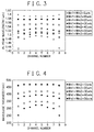
- the wavelength distribution in the array is substantially symmetric for channels 1 to 8 centered on channel 4 or 5.
- the central value of the inter-channel distribution of PL peak wavelengths can be varied from a short wavelength to a long wavelength, i.e., in a range of 100 nanometers (nm) or more by enlarging the SiO 2 mask width Wm.
- the waveguide layer thickness increases in association with increase of the SiO 2 mask width Wm.
- the layer thickness distribution is of almost the same shape as that of the PL peak wavelength shown in Fig. 3. It is therefore proved that the waveguide layer thickness can also be controlled by changing the SiO 2 mask width Wm.
- the PL intensity is kept at a high level in all channels, and the PL half-width is satisfactory narrow value.
- the abscissa and the ordinate respectively indicate the wavelength and the photoluminescence intensity.
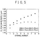
- the variation rate of the PL peak wavelength can be smoothed for channels 1 to 8 as shown in Fig. 5.
- the results support those obtained in the experiments shown in Fig. 3, namely, the mask width Wm is required to be equal to or slightly wider than Wa.
- Wa is also a parameter which also exerts a certain influence on the wavelength control of band gap in the MQW layer in the array.
- the degree of freedom of the band gap wavelength control for a crystal grown can be increased by appropriately changing the width W 0 of the array-shaped growth region (see Fig. 1) in a direction of the waveguide.
- the thickness of the crystal grown is increased, so its composition is shifted toward the long wavelength.
- the narrow-width micro-array selective growth of the present invention is carried out primarily through two physical phenomena, i.e., 1) effect of diffusion of source material and 2) effect of migration of source material.
- the effect of 1) can be efficiently used by setting the array interval of the micro-array to be fully less than the diffusion length of the material source.
- the array interval is setting to not more than 50 ⁇ m. It is therefore possible to uniformly control the crystal composition and the layer thickness for all channels of the array.
- the effect of 2) can be efficiently utilized by setting the width of the micro-array growth region to be fully less than the migration length of the source material, for example, the width is 10 ⁇ m or less such as 1.5 ⁇ m.
- the flatness of the layer of crystal selectively grown is improved.
- the band gap wavelength of each channel as shown in Fig. 4 can be independently controlled.
- the array waveguide formed by the crystal selectively grown satisfies the single transverse mode condition without changing the size thereof. Consequently, 1) the micro-array waveguide can be fabricated without etching the semiconductor and hence the yield is remarkably improved. Moreover, 2) a side surface of the crystal selectively grown is a smooth (111)B plane as shown in Fig. 2 and hence there is obtained an advantage that the light signal loss is conspicuously lowered when compared with the conventional waveguide which are fabricated by etching and which has consequently a rough surface.
- the results of these experiments above indicate that the narrow-width micro-array selective growth technology of the present invention makes it possible to manufacture an array light source in a very high integration density in a region in which one light source is conventionally fabricated at an interval of 250 ⁇ m.
- the array light source includes a plurality of optical waveguides which are mutually different in crystal composition appropriately controlled.
- the array-structured semiconductor optical devices can be fabricated on one wafer, the number of the devices being equal to the number of chips of the conventional single optical devices.
- the integration density becomes ten times or more that of the conventional integrated optical device.
- the present invention is therefore a quite effective technology to practically implement an array-structured semiconductor optical device in ultra-high integration.
- the band gap energy and the layer thickness of the crystal grown are controlled, using a dielectric thin film of width Wa formed between crystal growth regions, and two outer-most dielectric thin films formed at outer-most sides with widths W m1 and W m2 (W m1 , W m2 > Wa), respectively.
- an array-structured semiconductor optical device of the present invention is applied to a micro-array distribution feedback (DFB) type of semiconductor laser.
- Fig. 8 shows a layout of diffraction gratings
- Fig. 9 is a plan view of masks
- Fig. 10 shows cross-sectional views for explaining a semiconductor laser layer structure of each channel of an array.
- the DFB type semiconductor laser 100 (to be simply called “semiconductor laser” hereinafter) of this embodiment is that of a semiconductor laser of this type in which the detuning, ie. the difference between the gain peak wavelength of the laser and the Bragg wavelength of the diffraction grating, is adjusted to an appropriate value of ⁇ 10 nm.
- the semiconductor laser 100 has a laminated structure comprising, on an n-type InP substrate 99, a 1.13 ⁇ m n-type InGaAsP semiconductor layer 11, an n-type InP spacer layer 12, a 1.20 ⁇ m n-type InGaAsP light confining layer 13, a 7-film multi-quantum well layer 14 (1.50 ⁇ m InGaAsP well with compressive strain/1.20 ⁇ m InGaAsP barrier), a 1.20 ⁇ m InGaAsP light confining layer 15, and a p-type InP layer 16.
- the semiconductor laser 100 further includes on the laminated structure a p-type InP embedded clad layer 17 with a layer thickness of 2.0 ⁇ m a 0.3 ⁇ m thick p + -type InGaAs contact layer 18, an SiO 2 protective layer 19, a Cr/Au upper electrode 20 on an upper location, and a Cr/Au lower electrode 21 on a rear location.
- a diffraction grating pattern 88 is drawn by electron beam exposure and the like in a region on the n-type InP substrate 99 in a transversal direction for eight channels with an interval of 11.5 ⁇ m therebetween, each channel being 5 ⁇ m wide and 300 ⁇ m long.
- the period ⁇ 1 of the diffraction grating of channel 1 is set to 240 nm and the period is incrementally assigned to the other gratings with an increment of 0.625 nm, namely, the period ⁇ 8 of the diffraction grating of channel 1 is accordingly set to 245 nm in the process above.
- the diffraction grating pattern 88 is then copied onto the n-type InP substrate 99 by ordinary wet etching to fabricate a 60 nm deep diffraction grating 88.
- an SiO 2 masks 2 to 4 are then formed in a direction of ⁇ 011 ⁇ for selective growth as shown in Fig. 9.
- a 25 ⁇ m wide SiO 2 mask 5 is formed on both edge surfaces of the resonator.
- a 1.13 ⁇ m n-type InGaAsP semiconductor layer 11, an n-type InP spacer layer 12, a 1.20 ⁇ m n-type InGaAsP light confining layer 13 with, a 7-film multi-quantum well (MQW) layer 14 (1.50 ⁇ m InGaAsP well with compressive strain/1.20 ⁇ m InGaAsP barrier), a 1.20 ⁇ m InGaAsP light confining layer 15, and p-type InP layer 16 are fabricated by MOVPE or the like in accordance with the composition of each semiconductor layer in the layer direction shown in the cross-sectional views of Fig. 10. The layers are grown under a pressure of 150 Torr at a temperature of 650°.
- the photoluminescence (PL) peak wavelength of the MQW layer 14 can be changed from 1535 nm to 1570 nm for channels 1 to 8. Consequently, the gain peak wavelength of the MQW layer 14 can be changed to follow the oscillation wavelength of each channel determined by the period ⁇ of the diffraction grating. Namely, the detuning quantity, i.e., the discrepancy between the oscillation wavelength and the gain peak wavelength can be favorably retained within an appropriate value range of ⁇ 10 nm.
- a growth preventing mask is again formed to change the mask opening W 0 from 1.5 ⁇ m to 5 ⁇ m in the overall region.
- a 2.0 ⁇ m thick p-type InP embedded clad layer 17 and a 0.3 ⁇ m thick p + -type InGaAs contact layer 18 are selectively grown by MOVPE.
- MOVPE MOVPE
- an SiO 2 layer is fabricated on the overall surface to form current injection windows and a Cr/Au upper electrode 20 and a Cr/Au lower electrode 21 are manufactured by ordinary sputtering or the like.
- a device portion having a resonator length of 350 ⁇ m is cleaved and then a low-reflection coating SiON film is applied on both edge surfaces thereof by ordinary sputtering to complete the device.
- the size of the overall chip size is quite small, i.e., about 100 ⁇ m x 350 ⁇ m, there is manufactured a different wavelength DFB laser array in which each DFB laser of the array is independently detuned.
- an array-structured semiconductor optical device of the present invention is applied to a micro-array different wavelength semiconductor laser.
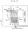
- Fig. 11 shows masks of the embodiment
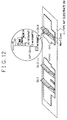
- Fig. 12 shows composition of each semiconductor layer of a laminated structure of the embodiment
- Fig. 13 shows in a partial perspective cross sectional view a configuration of the semiconductor laser.
- the semiconductor laser 200 of this embodiment is a micro-array different wavelength semiconductor laser including a spot size converter (SSC) in which each channel includes a laminated structure of layer composition shown in Fig. 12.
- the laser 200 has an overall construction shown in Fig. 13.
- the semiconductor laser device is of the same configuration as the device of the embodiment 1 excepting that the p-type InP embedded clad layer 17 has a layer thickness of 5.0 ⁇ m.
- SiO 2 masks 2 to 4 are formed on an n-type InP substrate 99 in a direction of ⁇ 011 ⁇ for selective growth by a stepper or the like as shown in Fig. 11.
- the masks 2 to 4 enclose eight array-like growth regions with an array interval of 20 ⁇ m, each growth region having an opening width W 0 of 1.5 ⁇ m.
- W m3 7 ⁇ m.
- optical waveguide layer shown in Fig: 12 are selectively grown by MOVPE under a pressure of 70 Torr at a temperature of 650°C.
- the laminated configuration includes a 1.13 ⁇ m n-type InGaAsP semiconductor layer 11, an n-type InP spacer layer 12, a 1.20 ⁇ m n-type InGaAsP light confining layer 13, a 7-film multi-quantum well (MQW) layer 14 (1.50 ⁇ m n-type InGaAsP well with compressive strain/1.20 ⁇ m InGaAsP barrier), a 1.20 ⁇ m InGaAsP light confining layer 15, and a p-type InP layer 16.
- MQW multi-quantum well
- the overall layer thickness of the waveguide layer distributes through a range of from 0.25 ⁇ m to 0.35 ⁇ m for channels 1 to 8 in the laser region and from 0.08 ⁇ m to 0.1 ⁇ m for channels 1 to 8 in the SSC region.
- the photoluminescence peak wavelength of the MQW layer can be changed in a range of from 1540 nm to 1590 nm for channels 1 to 8.
- a growth prevention mask is again formed with the mask opening width W 0 changed from 1.5 ⁇ m to 12 ⁇ m in the overall region.
- a 5.0 ⁇ m thick p-type InP embedded clad layer 17 and a 0.3 ⁇ m thick p + -type InGaAs contact layer 18 are grown by MOVPE.
- an SiO 2 layer is then fabricated to form current injection windows and a Cr/Au upper electrode 20 and a Cr/Au lower electrode 21 are manufactured in a usual sputtering process or the like.
- each resonator has a laser region length of 400 ⁇ m and an SSC region length of 200 ⁇ m.
- a high-reflection coating SiON film 22 is then fabricated on both edge surfaces of the laser by ordinary sputtering to thereby complete the device.
- the oscillation wavelength can be distributed through a range of from 1540 nm to 1590 nm for the channels of the laser array. Additionally, the threshold current characteristic is quite favorable and uniform, i.e., 6 mA ⁇ 1 mA and the single-side light output power is also satisfactorily obtained as 30 mW or more at a temperature of 25°C.
- an array-structured semiconductor optical device of the present invention is applied to a micro-array semiconductor optical amplifier including a spot size converter.
- Fig. 14 shows in a plan view masks of the embodiment 3
- Fig. 15 shows composition of each semiconductor layer in a laminated configuration of the array-structured semiconductor optical device
- Fig. 16 partly shows in a perspective cross sectional view the structure of the semiconductor laser.
- the optical amplifier 300 of the present embodiment is a micro-array semiconductor optical amplifier including a spot size converter.
- Each channel of the optical amplifier includes a laminated structure of composition shown in Fig. 15 and has an overall construction shown in Fig. 16. That is, as shown in Figs. 15 and 16, the optical amplifier 300 includes an n-type InP substrate 99 on which a 0.2 ⁇ m thick n-type InP buffer layer 24, a 0.4 ⁇ m thick 1.50 ⁇ m InGaAsP bulk active layer 25 with compressive strain, and a p-type InP layer 16 are fabricated in a laminated structure.
- the optical amplifier 300 further includes an SiO 2 protective layer 19 on the overall surface of the substrate, a Cr/Au upper electrode 20 on an upper surface thereof, and a Cr/Au lower electrode 21 on a lower surface thereof.
- the width W 0 of the SiO 2 mask growing region used for the narrow-width micro-array selective growth is set to 1.5 ⁇ m and a multi-quantum well layer is employed as the active layer.
- the growth region width W 0 is set to 0.6 ⁇ m, and an InGaAs bulk layer is used as the active layer.
- a micro-array semiconductor optical amplifier including a spot side converter can be easily manufactured through processes which are almost the same as those used in the embodiment 2.
- SiO 2 masks 2 to 4 are fabricated on an n-type InP substrate 99 in a direction of ⁇ 011 ⁇ with an array interval of 20 ⁇ m.
- the width W m2 of SiO 2 mask 2 is 1 ⁇ m in the SSC region, namely, is less than the array interval of 20 ⁇ m and hence a dummy growth region 77 is disposed between the growth regions of the respective channels.
- a 25 ⁇ m wide SiO 2 mask 5 is arranged on both end surfaces of the resonator.
- a laminated structure is grown with composition of each layer as shown in Fig. 15. Specifically, a 0.2 ⁇ m thick n-type InP buffer layer 24, a 0.4 ⁇ m thick 1.50 ⁇ m InGaAsP bulk active layer 25 with compressive strain, and a p-type InP layer 16 are selectively grown by MOVPE or the like under a pressure of 300 Torr at a temperature of 650°C.
- the photoluminescence peak wavelength of the bulk layer in the amplifier region can be kept almost retained in a range of from 1550 nm to 1570 nm for channels 1 to 8. Moreover, in the SSC region, the photoluminescence peak wavelength of the bulk layer is uniformly obtained in a range of from 1380 nm to 1390 nm for channels 1 to 8. Namely, the wavelength is sufficiently minimized for a low-loss passive waveguide having a spot size converter function. For all channels, the thickness of the InGaAsP bulk layer in the SSC region is advantageously reduced to at least 1/4 that of the layer thickness of the InGaAsP bulk layer in the amplifier region.
- the SiO 2 masks 2 to 4 are again formed with the mask opening width W 0 changed from 0.6 ⁇ m to 12 ⁇ m in the overall region. Utilizing the masks, a 5.0 ⁇ m thick p-type InP embedded clad layer 17 and a 0.3 ⁇ m thick p + -type InGaAs contact layer 18 are grown by MOVPE.
- an SiO 2 layer 19 is fabricated on the entire surface to form current injection windows and a Cr/Au upper electrode 20 and a Cr/Au lower electrode 21 are manufactured in an ordinary sputtering process or the like.
- a resonator region having a length of 1150 ⁇ m is cleaved and then a low-reflection coating SiON film 23 is fabricated on both edge surfaces.
- an 8-channel array semiconductor optical amplifier including a spot size converter in quite a small size of 160 ⁇ m x 1150 ⁇ m.
- optical amplifier there are obtained acceptable characteristics for all channels, i.e., an optical gain of 10 dB ⁇ 0.2 dB for an incident light having a wavelength of 1560 nm with a current of 30 mA injected to the amplifier and a coupling loss with a flat end optical fiber of 3.5 dB dB ⁇ 1 dB.
- the selectively grown waveguide has a lateral cross section having substantially a square contour and hence the gain characteristic of the amplifier is independent of polarization with respect to the transverse electric (TE) wave and the transverse magnetic (TM) wave.
- an array-structured semiconductor optical device of the present invention is applied to a micro-array wavelength selective light source.
- Fig. 17 shows a layout of a diffraction grating
- Fig. 18 is a plan view of masks of the embodiment 4
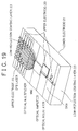
- Fig. 19 shows in a perspective view a configuration of the wavelength selective light source.
- the optical amplifier 400 of the present embodiment is an ultra-small-sized wavelength selective light source in the form of a monolithic integrated circuit on an InP substrate and primarily includes five regions as shown in Fig. 19.
- the light source 400 includes 1) a DFB laser region, 2) an optical multiplexer region, 3) a multimode interference region, 4) an optical amplifier region, and 5) an optical modulator region.
- a diffraction grating pattern 88 is drawn only in the DFB laser region on an n-type InP substrate 99 by an electron beam exposing process. Specifically, a 5 ⁇ m wide, 400 ⁇ m long line is drawn for each array in a lateral direction for each of the eight channels with an interval of 11.5 ⁇ m therebetween.
- the diffraction grating of channel 1 has a period ⁇ 1 of 240 nm, and the period is incremented by 0.25 nm for each of the gratings of the other channels.
- the grating of channel 8 has a period ⁇ 8 of 241.75 nm.
- the grating pattern 88 is copied onto the n-type InP substrate 99 by ordinary wet etching or the like to fabricate eight diffraction gratings 88 having a depth of 60 nm.
- SiO 2 masks are grown for selective growth.
- a 25 ⁇ m wide SiO 2 mask 5 is formed on the end surfaces thereof.
- a laminated structure similar to that of the embodiment 1 shown in Fig. 10 is selectively grown by MOVPE or the like.
- the lamination includes a 1.13 ⁇ m n-type InGaAsP semiconductor layer 11, an n-type InP spacer layer 12, a 1.20 ⁇ m n-type InGaAsP light confining layer 13, a 7-film MQW layer 14 (1.50 ⁇ m InGaAsP well with compressive strain/1.20 ⁇ m InGaAsP barrier), a 1.20 ⁇ m InGaAsP light confining layer 15, and a p-type InP layer 16.
- the growing process is carried out under a condition of 150 Torr and 650°C.
- the photoluminescence peak wavelength of the MQW layer was obtained as follows. 1) The wavelength can be changed in a range of from 1535 nm to 1550 nm for channels 1 to 8 in the DFB laser region; 2) the PL peak wavelength is 1380 nm for all channels in the optical multiplexer region; 3) 1300 nm in the MMI region; 4) 1542 nm in the optical amplifier region; and 5) 1472 nm in the optical modulator region.
- the gain peak wavelength of the MQW layer can be changed to follow the oscillation wavelength of each channel determined by the period of the diffraction grating. Namely, the detuning quantity (discrepancy between the oscillation wavelength and the gain peak wavelength) can be adjusted to a favorable value of ⁇ 10 nm or less for each channel.
- the SiO 2 masks are again formed with the mask opening width W 0 changed from 1.5 ⁇ m to 5 ⁇ m in 1) DFB laser region, 2) optical amplifier region, and 3) optical modulator region.
- the SiO 2 mask is completely removed from 4) MMI region.
- the SiO 2 mask is again formed to cover the W 0 wide growth region.
- a embedded waveguide structure is formed by MOVPE in almost the same structure as for the embodiment 1 shown in Fig. 10. That is; the structure including a 3 ⁇ m thick p-type InP embedded clad layer 17 and a 0.3 ⁇ m thick p + -type InGaAs contact layer 18.
- an embedded waveguide structure is manufactured in 1) DFB laser region, 2) optical amplifier region, 3) optical modulator region, and 4) MMI region and a high mesa waveguide structure are fabricated in 5) optical multiplexer region.
- an SiO 2 layer 19 is grown on the entire surface, a current injection windows are grown on an DFB laser region only, and a Cr/Au upper electrode 20 as well as a Cr/Au lower electrode 21 as prescribed are manufactured in an ordinary sputtering process or the like.
- a Cr/Au upper electrode 20 is again manufactured. Namely, to prevent the electrodes of the respective channels from being brought into contact with each other, there is provided a double electrode structure of the electrode 20.
- a resonator region having a length of 1500 ⁇ m is cleaved and then a low-reflection coating SiON film 23 is formed on both edge surfaces of the cleaved item in an ordinary sputtering or the like.
- a wavelength selective light source with quite a small size, i.e., the overall chip size is 80 ⁇ m x 1500 ⁇ m.
- the optical modulator has a modulation characteristic of 2.5 Gbits/s-600 Km transmission for the oscillation wavelengths of all channels.
- a single-mode oscillation can be obtained in each channel, and the yield is advantageously 50% or more.
- the semiconductor laser of micro-array distribution feedback (DFB) type is detuned to an appropriate value of ⁇ 10 nm.
- the present invention can be effectively employed even when the DFB laser of the first embodiment is replaced with a DBR laser, a DR laser, a laser of gain coupling type, or the like.
- the present invention is effectively applicable even when the semiconductor laser of the second embodiment is substituted to a DFB laser including a diffraction grating, a DBR laser, a DR laser, a laser of gain coupling type, or the like.
- the micro-array semiconductor optical amplifier including a spot size converter described as the third embodiment of the present invention can be coupled with an optical fiber or the like with a low coupling loss. Consequently, when the optical amplifier is combined with a fiber grating to form a single-mode laser of external resonator type, the overall device size can be quite efficiently minimized.
- the optical amplifier can be quite effectively used with such a PLC in a hybrid configuration to form a functional device.
- PLC planar lightwave circuit
- the micro-array semiconductor amplifier of the third embodiment is combined in a hybrid configuration with a quartz-based PLC including diffraction gratings having mutually different period described in "1997 IEICE Electronics Society Transactions 1 C-3- 103"
- the present invention is also efficiently utilized to manufacture a semiconductor laser array in which lights propagating through optical waveguides of the array mutually interfere with each other to thereby cause the array to oscillated as the whose in one transverse mode, i.e., a super-mode.
- the present invention has been described in relation to an example in which a waveguide is selectively grown with the opening width of the SiO 2 mask set to 1.5 ⁇ m.
- the present invention can also be efficiently applied to a selective growth process in which the selective growth SiO 2 mask includes an opening width exceeding 1.5 ⁇ m.
- the array size is remarkably minimized by particularly and appropriately adjusting the widths of the dielectric thin layers.
- the composition and the layer thickness vary between the adjacent waveguides of the array, which advantageously leads to a semiconductor waveguide array having a uniform optical device characteristic. Therefore, in accordance with the method of manufacturing the semiconductor waveguide array and the array-structured semiconductor optical device of the present invention, there is attained a super-high integration density so that array size is reduced to 1/10 or less when compared with the conventional method and device. This means that the yield of any array-structured semiconductor optical devices per wafer is improved to ten times that of the prior art and hence the present invention can be advantageously put to practices to supply such array-structured semiconductor optical devices at a low cost.
- the band gap energy of each waveguide layer of the array can be arbitrarily controlled, for example, the energy can be uniformly or linearly changed. Consequently, it is possible to uniform and improve characteristics of the array-structured semiconductor optical device including diffraction gratings and the like in a super-high integration.
Landscapes
- Physics & Mathematics (AREA)
- General Physics & Mathematics (AREA)
- Optics & Photonics (AREA)
- Engineering & Computer Science (AREA)
- Microelectronics & Electronic Packaging (AREA)
- Condensed Matter Physics & Semiconductors (AREA)
- Electromagnetism (AREA)
- Semiconductor Lasers (AREA)
- Optical Integrated Circuits (AREA)
Applications Claiming Priority (2)
| Application Number | Priority Date | Filing Date | Title |
|---|---|---|---|
| JP11305198 | 1998-04-23 | ||
| JP11305198 | 1998-04-23 |
Publications (2)
| Publication Number | Publication Date |
|---|---|
| EP0952470A2 true EP0952470A2 (de) | 1999-10-27 |
| EP0952470A3 EP0952470A3 (de) | 2004-01-14 |
Family
ID=14602263
Family Applications (1)
| Application Number | Title | Priority Date | Filing Date |
|---|---|---|---|
| EP99107362A Withdrawn EP0952470A3 (de) | 1998-04-23 | 1999-04-22 | Verfahren zur Herstellung einen optischen Vielfachhalbleiterwellenleiter und einer vielfachstrukturierten optische Halbleitervorrichtung |
Country Status (3)
| Country | Link |
|---|---|
| US (2) | US6228670B1 (de) |
| EP (1) | EP0952470A3 (de) |
| CA (1) | CA2269872A1 (de) |
Cited By (7)
| Publication number | Priority date | Publication date | Assignee | Title |
|---|---|---|---|---|
| WO2002049172A1 (en) * | 2000-12-15 | 2002-06-20 | The Furukawa Electric Co., Ltd | Semiconductor laser element, semiconductor laser module and production method therefor and optical fiber amplifier |
| EP1130706A3 (de) * | 2000-02-25 | 2002-10-16 | Nec Corporation | Optische Halbleitervorrichtung und Herstellungsverfahren |
| WO2003049160A3 (en) * | 2001-11-30 | 2003-12-18 | Epiic Ltd | Method of producing integrated semiconductor components on a semiconductor substrate |
| EP1130714A3 (de) * | 1999-12-28 | 2004-03-03 | NEC Compound Semiconductor Devices, Ltd. | Laserelemente mit verschiedenen Wellenlängen auf einem Substrat |
| EP1536532A1 (de) * | 2003-11-25 | 2005-06-01 | Fanuc Ltd | Halbleiterlaservorrichtung |
| EP1742314A2 (de) | 2005-06-16 | 2007-01-10 | Avago Technologies Fiber IP (Singapore) Pte. Ltd. | Begrabene Heterostrukturvorrichtung mit integriertem Wellenleitergitter hergestellt mit einstüfigen MOCVD |
| WO2020157741A1 (en) * | 2019-01-28 | 2020-08-06 | B.G. Negev Technologies & Applications Ltd., At Ben-Gurion University | Structure for a waveguide facet |
Families Citing this family (16)
| Publication number | Priority date | Publication date | Assignee | Title |
|---|---|---|---|---|
| US7095770B2 (en) * | 2001-12-20 | 2006-08-22 | Finisar Corporation | Vertical cavity surface emitting laser including indium, antimony and nitrogen in the active region |
| JP2001168450A (ja) * | 1999-09-28 | 2001-06-22 | Sharp Corp | 半導体レーザ素子およびそれを使用した電子機器 |
| JP2002164608A (ja) * | 2000-11-27 | 2002-06-07 | Mitsubishi Electric Corp | 光半導体装置およびその製造方法 |
| EP1458069A1 (de) * | 2003-03-12 | 2004-09-15 | Agilent Technologies, Inc. - a Delaware corporation - | Breit abstimmbare Laser Quelle mit verteilten Bragg-Reflektor |
| US7215852B2 (en) * | 2003-08-15 | 2007-05-08 | Lucent Technologies Inc. | Method and apparatus for mode conversion |
| JP4440697B2 (ja) * | 2004-04-22 | 2010-03-24 | 浜松ホトニクス株式会社 | 光導波路基板及びその製造方法 |
| US7860137B2 (en) * | 2004-10-01 | 2010-12-28 | Finisar Corporation | Vertical cavity surface emitting laser with undoped top mirror |
| WO2006039341A2 (en) * | 2004-10-01 | 2006-04-13 | Finisar Corporation | Vertical cavity surface emitting laser having multiple top-side contacts |
| KR100800664B1 (ko) * | 2006-04-04 | 2008-02-01 | 삼성전자주식회사 | 레이저 광 모듈 |
| CN101529292B (zh) * | 2006-07-31 | 2011-11-09 | 奥尼奇普菲托尼克斯有限公司 | 使用锥形波导的集成垂直波长(去)复用器 |
| JP5268733B2 (ja) * | 2009-03-25 | 2013-08-21 | 富士通株式会社 | 光導波素子とその製造方法、半導体素子、レーザモジュール及び光伝送システム |
| US8216866B2 (en) * | 2010-10-13 | 2012-07-10 | Sumitomo Electric Industries, Ltd. | Method to manufacture semiconductor device with optical grating |
| JP2012248812A (ja) * | 2011-05-31 | 2012-12-13 | Sumitomo Electric Ind Ltd | 半導体光集積素子の製造方法 |
| US20140198377A1 (en) * | 2013-01-15 | 2014-07-17 | Omron Corporation | Laser oscillator |
| US9698564B1 (en) * | 2016-02-09 | 2017-07-04 | Oracle International Corporation | Hybrid integrated MCM with waveguide-fiber connector |
| US11362487B2 (en) * | 2020-05-27 | 2022-06-14 | Microsoft Technology Licensing, Llc | Laser emitter including nanowires |
Family Cites Families (12)
| Publication number | Priority date | Publication date | Assignee | Title |
|---|---|---|---|---|
| US5157796A (en) * | 1991-08-12 | 1992-10-27 | Boyer Jacques F | Double flush toilet valve |
| EP0606093B1 (de) * | 1993-01-07 | 1997-12-17 | Nec Corporation | Integrierte optische Halbleiteranordnung und Herstellungsverfahren |
| JP2655498B2 (ja) | 1994-11-28 | 1997-09-17 | 日本電気株式会社 | 半導体レーザアレイの製造方法 |
| FR2727768B1 (fr) * | 1994-12-05 | 1997-01-10 | Alcatel Nv | Procede pour former une couche de silice a eliminer ulterieurement et procede pour rapporter un composant en optique integree |
| US5633966A (en) * | 1995-04-07 | 1997-05-27 | Sumitomo Electric Industries, Ltd. | Method of forming refractive index distribution in light transmission path, and optical filter and method of using the same |
| EP0782017B1 (de) * | 1995-12-28 | 2009-08-05 | Panasonic Corporation | Optischer Wellenleiter, Vorrichtung zur Umwandlung optischer Wellenlängen und Verfahren zu ihrer Herstellung |
| JPH1075009A (ja) * | 1996-08-30 | 1998-03-17 | Nec Corp | 光半導体装置とその製造方法 |
| US5914694A (en) * | 1996-09-19 | 1999-06-22 | Cal Corporation | Dual-band, dual polarization radiating structure |
| JPH10117040A (ja) * | 1996-10-08 | 1998-05-06 | Nec Corp | 半導体レーザ素子及びその製造方法 |
| KR100288742B1 (ko) * | 1997-03-12 | 2001-05-02 | 윤종용 | 광도파로소자의제조방법 |
| US5995055A (en) * | 1997-06-30 | 1999-11-30 | Raytheon Company | Planar antenna radiating structure having quasi-scan, frequency-independent driving-point impedance |
| JP3045115B2 (ja) * | 1997-09-30 | 2000-05-29 | 日本電気株式会社 | 光半導体装置の製造方法 |
-
1999
- 1999-04-22 US US09/298,229 patent/US6228670B1/en not_active Expired - Lifetime
- 1999-04-22 EP EP99107362A patent/EP0952470A3/de not_active Withdrawn
- 1999-04-22 CA CA002269872A patent/CA2269872A1/en not_active Abandoned
-
2001
- 2001-01-26 US US09/769,346 patent/US20010008539A1/en not_active Abandoned
Cited By (14)
| Publication number | Priority date | Publication date | Assignee | Title |
|---|---|---|---|---|
| EP1130714A3 (de) * | 1999-12-28 | 2004-03-03 | NEC Compound Semiconductor Devices, Ltd. | Laserelemente mit verschiedenen Wellenlängen auf einem Substrat |
| EP1130706A3 (de) * | 2000-02-25 | 2002-10-16 | Nec Corporation | Optische Halbleitervorrichtung und Herstellungsverfahren |
| US6828589B2 (en) | 2000-02-25 | 2004-12-07 | Nec Compound Conductor Devices, Ltd. | Optical semiconductor device and method for manufacturing the same |
| EP1258954A4 (de) * | 2000-12-15 | 2005-12-07 | Furukawa Electric Co Ltd | Halbleiter-laserelement, halbleiter-lasermodul und herstellungsverfahren dafür und faseroptischer verstärker |
| WO2002049172A1 (en) * | 2000-12-15 | 2002-06-20 | The Furukawa Electric Co., Ltd | Semiconductor laser element, semiconductor laser module and production method therefor and optical fiber amplifier |
| WO2003049160A3 (en) * | 2001-11-30 | 2003-12-18 | Epiic Ltd | Method of producing integrated semiconductor components on a semiconductor substrate |
| US7226849B2 (en) | 2001-11-30 | 2007-06-05 | Epiic Limited | Method of producing integrated semiconductor components on a semiconductor substrate |
| EP1536532A1 (de) * | 2003-11-25 | 2005-06-01 | Fanuc Ltd | Halbleiterlaservorrichtung |
| US7941024B2 (en) | 2004-02-25 | 2011-05-10 | Avago Technologies Fiber Ip (Singapore) Pte. Ltd | Buried heterostructure device having integrated waveguide grating fabricated by single step MOCVD |
| EP1742314A2 (de) | 2005-06-16 | 2007-01-10 | Avago Technologies Fiber IP (Singapore) Pte. Ltd. | Begrabene Heterostrukturvorrichtung mit integriertem Wellenleitergitter hergestellt mit einstüfigen MOCVD |
| EP1742314A3 (de) * | 2005-06-16 | 2008-11-12 | Avago Technologies Fiber IP (Singapore) Pte. Ltd. | Begrabene Heterostrukturvorrichtung mit integriertem Wellenleitergitter hergestellt mit einstüfigen MOCVD |
| CN1945365B (zh) * | 2005-06-16 | 2010-10-13 | 阿瓦戈科技光纤Ip(新加坡)股份有限公司 | 由单步mocvd制造的掩埋异质结构器件 |
| WO2020157741A1 (en) * | 2019-01-28 | 2020-08-06 | B.G. Negev Technologies & Applications Ltd., At Ben-Gurion University | Structure for a waveguide facet |
| US12055758B2 (en) | 2019-01-28 | 2024-08-06 | B.G. Negev Technologies & Applications Ltd., At Ben-Gurion University | Structure for a waveguide facet |
Also Published As
| Publication number | Publication date |
|---|---|
| US20010008539A1 (en) | 2001-07-19 |
| EP0952470A3 (de) | 2004-01-14 |
| US6228670B1 (en) | 2001-05-08 |
| CA2269872A1 (en) | 1999-10-23 |
Similar Documents
| Publication | Publication Date | Title |
|---|---|---|
| US6228670B1 (en) | Method of manufacturing a semiconductor optical waveguide array and an array-structured semiconductor optical device | |
| US5770466A (en) | Semiconductor optical integrated circuits and method for fabricating the same | |
| EP0665617A1 (de) | Abstimmbarer DBR laser mit alternierendem Gitter | |
| EP0735635A2 (de) | Optischer Halbleitervorrichtung, Antriebsverfahren und optisches Kommunikationssystem | |
| JPH10117040A (ja) | 半導体レーザ素子及びその製造方法 | |
| US6594298B2 (en) | Multi-wavelength semiconductor laser array and method for fabricating the same | |
| JP3336994B2 (ja) | 半導体光導波路アレイの製造方法及びアレイ構造半導体光素子 | |
| US5606573A (en) | Method and apparatus for control of lasing wavelength in distributed feedback lasers | |
| EP1104060B1 (de) | Optische Halbleitervorrichtung und zugehöriges Herstellungsverfahren | |
| JP2606078B2 (ja) | 半導体レーザアレイおよびその製造方法 | |
| EP0687938B1 (de) | Nicht-lineare optische Halbleitervorrichtung | |
| US20060203858A1 (en) | Wavelength tunable semiconductor laser apparatus | |
| EP0316194B1 (de) | Filter mit abstimmbarer Wellenlänge | |
| US6643315B2 (en) | Distributed feedback semiconductor laser device and multi-wavelength laser array | |
| JP2965011B2 (ja) | 半導体光素子及びその製造方法 | |
| US5675602A (en) | Optical integrated circuit device and driving method therefor | |
| JP2907234B2 (ja) | 半導体波長可変装置 | |
| JP2002289971A (ja) | 半導体光素子および半導体光素子の製造方法 | |
| US20210184427A1 (en) | Semiconductor Laser | |
| KR100377193B1 (ko) | 다파장 반도체 레이저 어레이 및 그의 제조 방법 | |
| JPH06283802A (ja) | 半導体レーザ装置及びその製造方法 | |
| JP4005519B2 (ja) | 半導体光装置及びその製造方法 | |
| JP2947702B2 (ja) | 波長可変レーザ装置およびその作製方法 | |
| Kudo et al. | 1.55-µm Wavelength-Selectable Microarray DFB-LD’s with Integrated MMI Combiner, SOA, and EA-Modulator | |
| JPH10154845A (ja) | 分布反射型半導体レーザアレイとその製造方法 |
Legal Events
| Date | Code | Title | Description |
|---|---|---|---|
| PUAI | Public reference made under article 153(3) epc to a published international application that has entered the european phase |
Free format text: ORIGINAL CODE: 0009012 |
|
| AK | Designated contracting states |
Kind code of ref document: A2 Designated state(s): AT BE CH CY DE DK ES FI FR GB GR IE IT LI LU MC NL PT SE |
|
| AX | Request for extension of the european patent |
Free format text: AL;LT;LV;MK;RO;SI |
|
| PUAL | Search report despatched |
Free format text: ORIGINAL CODE: 0009013 |
|
| AK | Designated contracting states |
Kind code of ref document: A3 Designated state(s): AT BE CH CY DE DK ES FI FR GB GR IE IT LI LU MC NL PT SE |
|
| AX | Request for extension of the european patent |
Extension state: AL LT LV MK RO SI |
|
| RIC1 | Information provided on ipc code assigned before grant |
Ipc: 7G 02B 6/12 B Ipc: 7H 01S 3/025 B Ipc: 7H 01S 3/25 B Ipc: 7G 02B 6/132 A |
|
| 17P | Request for examination filed |
Effective date: 20031202 |
|
| 17Q | First examination report despatched |
Effective date: 20040218 |
|
| AKX | Designation fees paid |
Designated state(s): DE FR NL |
|
| STAA | Information on the status of an ep patent application or granted ep patent |
Free format text: STATUS: THE APPLICATION IS DEEMED TO BE WITHDRAWN |
|
| 18D | Application deemed to be withdrawn |
Effective date: 20040629 |