EP0952548A2 - Méthode et appareil pour effectuer un arrondi à plusieurs niveaux et inspection de modèle - Google Patents
Méthode et appareil pour effectuer un arrondi à plusieurs niveaux et inspection de modèle Download PDFInfo
- Publication number
- EP0952548A2 EP0952548A2 EP99107654A EP99107654A EP0952548A2 EP 0952548 A2 EP0952548 A2 EP 0952548A2 EP 99107654 A EP99107654 A EP 99107654A EP 99107654 A EP99107654 A EP 99107654A EP 0952548 A2 EP0952548 A2 EP 0952548A2
- Authority
- EP
- European Patent Office
- Prior art keywords
- masking
- pattern
- pixel
- gradation
- corner
- Prior art date
- Legal status (The legal status is an assumption and is not a legal conclusion. Google has not performed a legal analysis and makes no representation as to the accuracy of the status listed.)
- Withdrawn
Links
Images


Classifications
-
- G—PHYSICS
- G06—COMPUTING OR CALCULATING; COUNTING
- G06T—IMAGE DATA PROCESSING OR GENERATION, IN GENERAL
- G06T7/00—Image analysis
- G06T7/0002—Inspection of images, e.g. flaw detection
- G06T7/0004—Industrial image inspection
- G06T7/001—Industrial image inspection using an image reference approach
-
- G—PHYSICS
- G06—COMPUTING OR CALCULATING; COUNTING
- G06T—IMAGE DATA PROCESSING OR GENERATION, IN GENERAL
- G06T2207/00—Indexing scheme for image analysis or image enhancement
- G06T2207/30—Subject of image; Context of image processing
- G06T2207/30108—Industrial image inspection
- G06T2207/30148—Semiconductor; IC; Wafer
Definitions
- the present invention relates in general to pattern inspection, and relates in particular to a method an apparatus for performing rounding correction of reference images used for Die-To-DataBASE inspection in terms of design data.
- This type of pattern inspection apparatus is required to first perform conversion of design data, coordinates of rectangular or trapezoidal shapes and line data described in stroke characters, into binary digital data comprised by [0]s and [1]s.
- an object pattern to be inspected is scanned with a laser beam, and using an image of the object pattern obtained either by transmitting light through the object pattern and focusing on a photodetector, or an optical imaging system, the characteristics of the edge profile of the object image are defined, and optical point-spread functions for the pattern are generated.
- the functions and binary bit data are convoluted to compute multi-level data (multi-valued data) which are used to produce a reference image.
- an actual image produced from optical scanning or imaging system and the reference image obtained from the design data are read synchronously into the apparatus to compare both images at the corresponding pixel locations, thereby detecting any discrepancies or defects in the actual image of the object pattern compared to the reference image of the same, according to Die-To-DataBASE protocol (detection test of defects in the actual pattern).
- an approach may be considered to examine the features in various inspection locations of the object pattern, so that the reference image can be corrected beforehand in appropriate ways to recognize corners or to properly detect edge positions.
- a corner shape in a reference image is corrected using a corner inspection process suitable to the actual image, leading to correcting the design data without changing their binary format and bit (pixel) units.
- corner shape modifications in the reference image are performed by first making a modified bit pattern based on the design bit pattern, and then performing logic computations using the binary bit data of the real image of the object pattern to carry out corrections for the corner shape in the reference image.
- correction templates in bit-units are prepared so as to match specific corner angles (for example, 0, 45, 90, 135 degrees) of the corners which are found in the design data.
- corner templates those which are closest to the corner shapes in the actual image are selected, and the original design data are corrected using the selected corner templates, and the modified design data are again processed to produce a final multi-valued image in 4-16 tonal gradations.
- the final reference image so produced are compared with the real image so that the differences in the tonal gradations in the final reference image and the actual image can be determined using a suitable threshold value of defect detection algorithm, to determine whether the discrepancies are functional defects.
- This type of inspection approach is outlined in Japanese Patent Applications, First Publications, Hei 4-350776 and Hei 6-273915.
- a problem inherent in the conventional method of pattern inspection is that the productivity is low.
- a reference image is produced first from the original design data, and using the templates to approximate the corners in the real image, the original design data are correct to produce another reference image.
- the final reference image closely duplicates the actual image produced by optical scanning, the overall process is cumbersome and suffers from low productivity. It also presents a problem of creating pseudo-defects during the processing, caused by the difference in the tone gradations between correction templates and the actual image. This will be explained in more detail.
- Correction templates for the design data are selected from many templates for matching of pattern shapes by selecting individual bit string patterns representing templates that are most similar to the string patterns in the actual image.
- Such computed bit strings are convoluted with point spread functions computed from the light intensity values obtained by optical scanning and the corrected template images to produce the final multi-valued reference image for comparison purposes. This process becomes highly computation-intensive when the number of pixels increase in an image, and consequently inspection productivity suffers.
- Another problem is that, because corner identify and gradation rounding adjustment processes are carried out separately for one expanded reference data, computation requirements are further increased.
- processing speed may be shortened by including corner information in the pre-expansion design information, but this method suffers from an enormous amount of design information, which leads to increase in memory resources and expansion time. The result is that the overall productivity of inspection is lowered.
- the existing method suffers from a drawback that the gradation values of the corrected pattern are limited by the gradation distribution available in the template.
- gradation correction is carried out without regard to the shapes of surrounding patterns, edge sections in a pattern that do not coincide with pixel locations and rounded sections extending from an edge to a corner are problematic, because the differences in gradation, between the reference image and the actual image obtained by scanning, become large, making such areas vulnerable to be identified as pseudo-defects.
- those defects in the object pattern existing in a pixel boundary or in corners that are smaller than the resolution capability of the inspection apparatus and are poor in contrast relative to the surrounding, are difficult to detect by comparing such patterns with the reference image, because they exhibit inferior difference in gradation relative to the surrounding.
- the object has been achieved in a method for a multi-level corner rounding process: where reference data are generated by expanding the design data so as to produce multi-level gradation reference data at each pixel having a resolution capability that is finer than an inspection resolution capability; the corner sections are automatically identified in the reference data that do not contain any corner information; and a corner rounding operation is performed on a corner section in a multi-level gradation state, in accordance with a corner radius extracted from the real image at a resolution finer than the inspection resolution capability.
- the method may also include a step in which a corner section in the reference data is corrected to approximate a shape of a corner section in the real image, by scanning over the multi-level reference data about an object pixel, with a circular masking, or a ring shaped masking or a polygonal masking approximating a circle, having a radius given in pixel units or sub-pixel units, so as to define a neighboring pixel range of the object pixel.
- the method may also include a step in which a corner pattern identification reference value for a masking pattern is derived according to a computational process comprising the steps of: defining a reference value for inside-masking total gradation derived by multiplying a maximum gradation value achievable in an object pattern in the reference data with a masking area ratio, which is a ratio of two areas, a unit area of a unit pixel and an area occupied in the unit pixel by a circular masking, or a ring-shaped masking or a polygonal masking defined in sub-pixel units, to be scanned into the reference data, and summing all products; designating one masking region that does not contain a center pixel produced by dividing the masking pattern along any line in the masking pattern, and similarly designating other masking region that contains the center pixel in the masking pattern; and assigning a masking curvature range lower limit value to the reference value of the inside-masking total gradation in the one masking region, while assigning a masking curva
- the method may also include step in which a 1-pixel gradation ratio is derived by dividing the maximum gradation value by a difference between a masking curvature range upper limit and a masking curvature range lower limit.
- the method may also include a step in which a gradation correction process for the object pattern comprises the steps of: obtaining an inside-masking total gradation value by multiplying a masking area ratio, which is a ratio of two areas, a unit area of a unit pixel and an area occupied in the unit pixel by a circular masking, a ring masking or a polygonal masking defined in sub-pixel units, to be scanned into reference data, with gradation values contained in the reference data at corresponding individual pixels inside the masking pattern, and summing all products; assigning a minimum gradation value as a gradation value of a center pixel address in the masking pattern, when an inside-masking total gradation value is less than a masking curvature range lower limit value; assigning a maximum gradation value as a gradation value of a center pixel address in the masking pattern, when an inside-masking total gradation value is greater than a masking curvature range upper limit value; assigning to
- the method may also include a step in which after completing rounding operations of corner sections, a comparison reference image is produced by applying a filtering process, suitable to optical properties of an inspection apparatus, to multi-level gradation reference data so as to produce the comparison reference image having gradations approximating gradations in corner sections in a corresponding real image.
- the multi-level corner rounding methods presented above are practiced most preferably in a pattern inspection apparatus for scanning an object pattern, generated according to design data, with a laser beam of a specific wavelength; focusing transmitted light on photodetector means through an objective lens so as to generate a real image from pattern information obtained from the photodetector means; comparing the real image with a reference image derived from the design data; and detecting defects in the object pattern.
- design data whose gradation values at each pixel are prepared as a matrix of high resolution multi-level gradations are corrected while maintaining the multi-level gradations. Therefore, even when the corner and edge sections of the design data are located inside a pixel, not at a pixel boundary, gradations in the corner sections in the object pattern can be expressed with a high degree of precision, thereby producing a reference image that closely matches the real image obtained from the object pattern.
- gradations in the multi-level expanded reference data are corrected using a suitable masking pattern based on a total value of the neighboring gradations of a target pixel located inside the masking pattern. Therefore, when matching the corner shape with a template, corrected gradations are not limited by the gradations available in the template as in the conventional method, thereby enabling to produce a reference image closely matching the gradations in the real image. Also, a masking pattern can be chosen in pixel units or sub-pixel units according to the radius of curvature of the corner sections in the real image, therefore, corner section gradations in the design data can be corrected to suit the degree of precision required in individual inspection.
- the present method not only the shape of a making pattern but the 1-pixel gradation ratio can be adjusted by varying the masking curvature range, therefore, the present method enables to process those gradations that can not be corrected by shape correction alone.
- An additional advantage is that corner recognition and rounding operations can be performed concurrently in one scanning operation of the masking pattern into the reference data, thereby significantly increasing the inspection productivity.
- the method is able to significantly control distortion in the object pattern produced by the rounding process, thereby enabling to produce a reference image closely matching the real image, even when the scanning direction does not coincide with the order of arrangement of the design data.
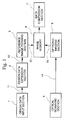
- Figure 1 is a block diagram of a first embodiment of the pattern inspection apparatus of the present invention.
- Figure 2 is an illustration of a part of an expanded pattern of a wiring corner.
- Figure 3 is an enlarged view of one pixel shown in Figure 2.
- Figure 4 is a tabular matrix to explain the gradation values of each pixel shown in Figure 2.
- Figure 5 is a diagram for a four-neighbor masking pattern defined in pixel units.
- Figure 7 is a diagram showing polygonal masking patterns (true circle) with various radii defined in sub-pixel units.
- Figure 8 is a diagram for a polygonal masking pattern shown in Figure 7, where the radius corresponds to 2.5 pixels.
- Figure 9 is a diagram for a ring masking pattern defined in sub-pixel units.
- Figure 11A ⁇ 11E are illustrations to explain how masking curvature range and 1-pixel gradation ratio are generated.
- Figure 12 is a flowchart for a multi-level rounding process.
- Figure 13A ⁇ 13D are illustrations to explain how to determine the gradation values in the corner rounding process based on pixel units.
- Figure 14A ⁇ 14F are illustrations of reference images after performing rounding processes using various masking shapes on a corner section of reference data.
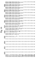
- Figure 15 is a tabular matrix to show a distribution of actual gradation values in a corner section in an actual image obtained by laser scanning.
- Figure 16 is a tabular matrix to show the results of performing a blending (gradation) operation after a corner rounding operation.
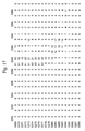
- Figure 17 is a tabular matrix to show a distribution of gradation values in a difference image between the actual image and the reference image.
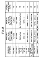
- Figure 18 is a table to show the numerical data of masking curvature upper limit, lower limit and 1-pixel gradation ratio for the masking patterns used in the present invention.
- Figure 1 is a block diagram of a first embodiment of the pattern inspection apparatus.
- the pattern inspection apparatus includes an optical scanning section 4 for scanning a wiring pattern (object pattern) to be inspected by a laser beam and outputting scan signals 14, and an optronic imaging section 5 for converting the scan signals 14 to an actual image 15 having multi-valued gradations.
- the apparatus also includes: a design data input section 1 for inputting design data 11 to define the shape and sizes of an object pattern to be inspected; a design data expansion section 2 for expanding the design data 11 into a wiring pattern to produce multi-level gradation reference data 12; a reference image forming section 3 for producing a reference image 13 by correcting individual wiring patterns in the reference data 12 so as to match the actual image 15; and a data comparison section 7 to perform inspection of the object pattern by comparing the actual image 15 produced by optical scanning with the reference image 13 produced from the design data 11.
- a design data input section 1 for inputting design data 11 to define the shape and sizes of an object pattern to be inspected
- a design data expansion section 2 for expanding the design data 11 into a wiring pattern to produce multi-level gradation reference data 12
- a reference image forming section 3 for producing a reference image 13 by correcting individual wiring patterns in the reference data 12 so as to match the actual image 15
- a data comparison section 7 to perform inspection of the object pattern by comparing the actual image 15 produced
- Design data 11 described in a format such as MEBES are input from the design data input section 11.
- input design data 11 are expanded in the design data expansion section 2, as a wiring pattern at individual pixels arranged in a lattice configuration to correspond to the coordinate addresses in the actual image 15.
- Figure 2 shows a portion of an expanded wiring pattern. Pixels are represented by each rectangle, and correspond to the expansion resolution capability of the design data expansion section 2.
- the edge 22 of a pattern 21 is not located at a pixel boundary, and indicates that, in a pixel 23, the pattern 21 occupies the pixel area in a ratio of 3:1 in x-direction (horizontal), and in a ratio of 1:1 in y-direction (vertical).
- Each pixel is provided with a plurality of sub-pixels for computing the values for multi-valued gradation (gray scale) at a finer resolution level than that given by the inspection resolution capability, so that the precision of the gradation levels is determined by the number of sub-pixels provided in each pixel.
- each pixel is comprised by 16 x 16 sub-pixels, where each sub-pixel represents a binary bit and can have a value of either [0] or [1].
- Figure 3 is an enlarged view of the pixel 23 shown in Figure 2. It can be seen that the pattern 21 occupies 8 x 12 sub-pixels among the total number of sub-pixels 16 x 16 available in one pixel.
- the gradation value of the pixels for the edge portion which occupies partial pixels in the pattern 21 is given by the number of sub-pixels in the individual pixels that are inside the pattern 21.
- gradation values of the expanded pattern 21 can be computed at each pixel representing an address of each coordinate point in the actual image 15.
- the reference image forming section 3 corrects for edge positions in the wiring pattern by enlarging or reducing the line width of the edge data included in the reference data 12, output from the design data expansion section 2, and appropriately moves the edge position on the basis of pixel units or sub-pixel units.
- a corner section in the reference data 12 and a corresponding corner section in the actual image 15 are compared, and the corner section in the reference data 12 is corrected to produce a multi-valued rounded corner based on the radius of the corner section in the actual image 15.
- correction parameters which are radius size for rounding and the number of times the rounding process to be repeated, are determined as follows.
- a representative actual image 15 is selected from the many actual images 15 stored in the image memory 6 (see Figure 1), and using an image of the target corner section, the shape and gradation distributions in the actual image 15 are examined in relation to the corresponding corner section in the object pattern in the reference data 12.
- the correction parameters are then determined according to the minimum value of the sum of the differences in the brightness between the real image 15 and the reference image 13, produced by modifying the reference data 12 at the corresponding corner using various shapes of masking patterns to closely match the corner characteristics in the real image 15. Detailed steps will be explained in the following.
- Figure 7 shows various examples of a polygonal pattern (true circle) having various radii defined in sub-pixel units
- Figure 9 is an example of a ring pattern defined in sub-pixel units
- each grid represents a unit pixel
- Representative masking pattern edges in the reference data 12 to be scanned are chosen such that they are not blended and their gradation values are all at MAX.
- a value for the curvature range lower limit is computed using the relation (1) shown below, and the computation process will be explained with reference to Figures 11.
- the lower limit is MAX x 8.
- the lower limit represents the highest number of gradations that can be exhibited inside a masking region that does not include the pixel array having the center pixel.
- curvature range upper limit value S2 x MAX
- the upper limit of curvature range is MAX x 13, as shown in Figure 11D.
- the upper limit represents the highest number of gradations achievable inside the masking region that includes the pixel array having the center pixel.
- a 1-pixel gradation ratio of the masking curvature range is computed according to relation (3), and is explained with reference to Figure 11E, which shows a process of pixel subtraction of the lower limit value from the maximum limit value of the masking curvature range.
- the 1-pixel gradation ratio is obtained by dividing the maximum gradation value (MAX) with the result of pixel subtraction.
- Figure 18 summarizes the results of computation of the upper and lower limit values of the masking curvature range, and the 1-pixel gradation ratio of the masking curvature range for the respective masking patterns shown in Figures 5 ⁇ 10 inclusively.
- the upper and lower limit values of the masking curvature range, the 1-pixel gradation ratio and the number of repetition of rounding process are pre-calculated using the shape of the actual masking pattern, and the results are stored in the memory in the reference image forming section 3 (step 51).
- the selected masking pattern is scanned over in the reference data 12.
- step 54 a value for the inside-masking total gradation is obtained (step 54), and depending on the value of the inside-masking total gradation so found, one of the following three steps is carried out to correct the gradation of the object pixel (step 55).
- Figure 13 shows an example of performing the rounding correction steps shown in Figure 12 on a circular masking pattern shown in Figure 6.
- Figure 14A shows an as-expanded reference image produced from the reference data 12
- Figures 14B to 14F show the results of applying each of the masking patterns shown in Figure 6, Figure 7 and Figure 9 to perform multi-level rounding process to the as-expanded reference image.
- Figure 15 shows the gradation values in a corner section in the real image
- Figure 16 shows the gradation values in a reference image 13 at the same corner after applying two stages of corrections to the real image 15.
- the corrected results of rounding were then further subjected to a blending (gradation) process using the filtering coefficients of optical point spread function obtained from the real image 15.
- Figure 17 shows gradation values in the various location of a difference image between the reference image 13 and the real image 15.
- the reference image forming section 3 produces a reference image 13, from the reference data 12 input thereto, by applying the multi-level rounding correction process at a pixel-unit level or a sub-pixel unit level, that is very close to the real image 15.
- the reference image 13 is stored in the image memory 6, and is compared with the actual image 15 which has already been stored, and the images are compared in the image comparison section 7 whether the object pattern for inspection is drawn accurately based on the ideal pattern produced from the respective design data including shape and size of the circuit.
- a true circle masking pattern can be used directly to increase the precision of pattern inspection even more.
Landscapes
- Engineering & Computer Science (AREA)
- Quality & Reliability (AREA)
- Computer Vision & Pattern Recognition (AREA)
- Physics & Mathematics (AREA)
- General Physics & Mathematics (AREA)
- Theoretical Computer Science (AREA)
- Investigating Materials By The Use Of Optical Means Adapted For Particular Applications (AREA)
- Image Processing (AREA)
- Length Measuring Devices By Optical Means (AREA)
- Image Analysis (AREA)
- Testing Or Measuring Of Semiconductors Or The Like (AREA)
Applications Claiming Priority (2)
| Application Number | Priority Date | Filing Date | Title |
|---|---|---|---|
| JP10752398 | 1998-04-17 | ||
| JP10107523A JP3028945B2 (ja) | 1998-04-17 | 1998-04-17 | 多階調丸め補正処理方法およびパターン検査装置 |
Publications (2)
| Publication Number | Publication Date |
|---|---|
| EP0952548A2 true EP0952548A2 (fr) | 1999-10-27 |
| EP0952548A3 EP0952548A3 (fr) | 2000-02-23 |
Family
ID=14461361
Family Applications (1)
| Application Number | Title | Priority Date | Filing Date |
|---|---|---|---|
| EP99107654A Withdrawn EP0952548A3 (fr) | 1998-04-17 | 1999-04-16 | Méthode et appareil pour effectuer un arrondi à plusieurs niveaux et inspection de modèle |
Country Status (3)
| Country | Link |
|---|---|
| US (1) | US6504947B1 (fr) |
| EP (1) | EP0952548A3 (fr) |
| JP (1) | JP3028945B2 (fr) |
Cited By (9)
| Publication number | Priority date | Publication date | Assignee | Title |
|---|---|---|---|---|
| GB2361309A (en) * | 1999-12-16 | 2001-10-17 | Nec Corp | Pattern inspection method and device |
| WO2006049243A1 (fr) * | 2004-11-05 | 2006-05-11 | Nec Corporation | Appareil de test de motif, méthode de test de motif et programme de test de motif |
| EP2199065A1 (fr) * | 2008-12-19 | 2010-06-23 | Agfa Graphics N.V. | Procédé de traitement d'images pour impression tridimensionnelle |
| CN101477065B (zh) * | 2009-01-08 | 2011-02-09 | 西安电子科技大学 | 基于缺陷边界值变化次数的ic缺陷分类方法 |
| CN103063164A (zh) * | 2012-12-15 | 2013-04-24 | 艾尼科环保技术(安徽)有限公司 | 机械零件r角小于0.5的简易测量方法 |
| CN104101308A (zh) * | 2014-06-16 | 2014-10-15 | 武汉市安曼特微显示科技有限公司 | 测量圆角的系统和方法 |
| CN102878907B (zh) * | 2012-09-20 | 2016-12-21 | 靖江量具有限公司 | 测量零件倒角角度卡尺 |
| CN110018181A (zh) * | 2019-04-25 | 2019-07-16 | 德淮半导体有限公司 | 一种晶圆缺陷检测的方法和装置 |
| CN117671545A (zh) * | 2024-01-31 | 2024-03-08 | 武汉华测卫星技术有限公司 | 一种基于无人机的水库巡检方法及系统 |
Families Citing this family (25)
| Publication number | Priority date | Publication date | Assignee | Title |
|---|---|---|---|---|
| US7796801B2 (en) * | 1999-08-26 | 2010-09-14 | Nanogeometry Research Inc. | Pattern inspection apparatus and method |
| US7817844B2 (en) * | 1999-08-26 | 2010-10-19 | Nanogeometry Research Inc. | Pattern inspection apparatus and method |
| DE60139047D1 (de) * | 2000-01-31 | 2009-08-06 | Omron Tateisi Electronics Co | Optischer verschiebungssensor |
| JP2001289614A (ja) * | 2000-01-31 | 2001-10-19 | Omron Corp | 変位センサ |
| US6775410B1 (en) * | 2000-05-25 | 2004-08-10 | Xerox Corporation | Image processing method for sharpening corners of text and line art |
| JP4044297B2 (ja) * | 2001-03-29 | 2008-02-06 | 株式会社東芝 | パターン欠陥検査装置 |
| US6848087B2 (en) * | 2001-05-30 | 2005-01-25 | Credence Systems Corporation | Sub-resolution alignment of images |
| JP3648495B2 (ja) * | 2002-05-21 | 2005-05-18 | 株式会社東芝 | 欠陥検査方法及びその装置 |
| US6867753B2 (en) * | 2002-10-28 | 2005-03-15 | University Of Washington | Virtual image registration in augmented display field |
| DE10257323A1 (de) * | 2002-12-06 | 2004-07-08 | Leica Microsystems Semiconductor Gmbh | Verfahren und Mikroskop zum Detektieren von Bildern eines Objekts |
| JP4076906B2 (ja) * | 2003-05-16 | 2008-04-16 | 株式会社トプコン | 外観検査方法 |
| JP4018642B2 (ja) * | 2004-01-05 | 2007-12-05 | 株式会社東芝 | 参照データ生成方法、パターン欠陥検査装置、パターン欠陥検査方法、及び参照データ生成プログラム |
| DE102005011344B4 (de) * | 2004-03-15 | 2014-02-13 | Omron Corporation | Sensorvorrichtung |
| JP4193760B2 (ja) * | 2004-06-29 | 2008-12-10 | 日本電気株式会社 | 画像パターン補正方法、及びそれを適用した模擬画像生成方法、並びにパターン外観検査方法 |
| JP4039423B2 (ja) * | 2004-12-14 | 2008-01-30 | 日産自動車株式会社 | エッジ位置算出装置、障害物検出システム |
| JP4901254B2 (ja) * | 2006-03-22 | 2012-03-21 | 株式会社日立ハイテクノロジーズ | パターンマッチング方法、及びパターンマッチングを行うためのコンピュータプログラム |
| JP5429869B2 (ja) * | 2008-12-22 | 2014-02-26 | 株式会社 Ngr | パターン検査装置および方法 |
| US8150140B2 (en) * | 2008-12-22 | 2012-04-03 | Ngr Inc. | System and method for a semiconductor lithographic process control using statistical information in defect identification |
| EP2586190A1 (fr) * | 2010-06-25 | 2013-05-01 | OCE-Technologies B.V. | Procédé pour améliorer des informations détaillées |
| US10102619B1 (en) | 2011-03-28 | 2018-10-16 | Hermes Microvision, Inc. | Inspection method and system |
| US9494856B1 (en) * | 2011-06-07 | 2016-11-15 | Hermes Microvision, Inc. | Method and system for fast inspecting defects |
| US10640961B2 (en) | 2012-12-19 | 2020-05-05 | Gmat Ventures, Llc | Water conservation based on toilet seat position |
| CN109000887B (zh) * | 2018-05-25 | 2021-04-23 | 京东方科技集团股份有限公司 | 一种图案检测装置及方法、图案化控制系统及方法 |
| CN111982925B (zh) * | 2019-05-24 | 2025-10-31 | 宁波群辉光电有限公司 | 检测方法及检测装置 |
| CN120010177B (zh) * | 2025-03-24 | 2025-10-28 | 常州维普半导体设备有限公司 | 一种掩模版通孔层方孔亮度优化的方法 |
Family Cites Families (7)
| Publication number | Priority date | Publication date | Assignee | Title |
|---|---|---|---|---|
| JPS59157505A (ja) * | 1983-02-28 | 1984-09-06 | Hitachi Ltd | パタ−ン検査装置 |
| JPS63211076A (ja) * | 1987-02-27 | 1988-09-01 | Hitachi Ltd | パタ−ン検査装置 |
| US4945351A (en) * | 1988-05-23 | 1990-07-31 | Hewlett-Packard Company | Technique for optimizing grayscale character displays |
| US5475766A (en) * | 1991-09-05 | 1995-12-12 | Kabushiki Kaisha Toshiba | Pattern inspection apparatus with corner rounding of reference pattern data |
| JPH06273915A (ja) | 1993-03-19 | 1994-09-30 | Fujitsu Ltd | 露光用レチクルのパターン検査方法 |
| US5804340A (en) * | 1996-12-23 | 1998-09-08 | Lsi Logic Corporation | Photomask inspection method and inspection tape therefor |
| US6091845A (en) * | 1998-02-24 | 2000-07-18 | Micron Technology, Inc. | Inspection technique of photomask |
-
1998
- 1998-04-17 JP JP10107523A patent/JP3028945B2/ja not_active Expired - Lifetime
-
1999
- 1999-04-15 US US09/291,944 patent/US6504947B1/en not_active Expired - Lifetime
- 1999-04-16 EP EP99107654A patent/EP0952548A3/fr not_active Withdrawn
Cited By (15)
| Publication number | Priority date | Publication date | Assignee | Title |
|---|---|---|---|---|
| GB2361309A (en) * | 1999-12-16 | 2001-10-17 | Nec Corp | Pattern inspection method and device |
| US7239735B2 (en) | 1999-12-16 | 2007-07-03 | Nec Corporation | Pattern inspection method and pattern inspection device |
| WO2006049243A1 (fr) * | 2004-11-05 | 2006-05-11 | Nec Corporation | Appareil de test de motif, méthode de test de motif et programme de test de motif |
| CN102256767A (zh) * | 2008-12-19 | 2011-11-23 | 爱克发印艺公司 | 用于三维印刷的图像处理方法 |
| WO2010079017A3 (fr) * | 2008-12-19 | 2010-09-10 | Agfa Graphics Nv | Procédé de traitement d'image pour impression tridimensionnelle |
| EP2199065A1 (fr) * | 2008-12-19 | 2010-06-23 | Agfa Graphics N.V. | Procédé de traitement d'images pour impression tridimensionnelle |
| US8705144B2 (en) | 2008-12-19 | 2014-04-22 | Agfa Graphics Nv | Image processing method for three-dimensional printing |
| CN102256767B (zh) * | 2008-12-19 | 2014-11-26 | 爱克发印艺公司 | 用于三维印刷的图像处理方法 |
| CN101477065B (zh) * | 2009-01-08 | 2011-02-09 | 西安电子科技大学 | 基于缺陷边界值变化次数的ic缺陷分类方法 |
| CN102878907B (zh) * | 2012-09-20 | 2016-12-21 | 靖江量具有限公司 | 测量零件倒角角度卡尺 |
| CN103063164A (zh) * | 2012-12-15 | 2013-04-24 | 艾尼科环保技术(安徽)有限公司 | 机械零件r角小于0.5的简易测量方法 |
| CN104101308A (zh) * | 2014-06-16 | 2014-10-15 | 武汉市安曼特微显示科技有限公司 | 测量圆角的系统和方法 |
| CN110018181A (zh) * | 2019-04-25 | 2019-07-16 | 德淮半导体有限公司 | 一种晶圆缺陷检测的方法和装置 |
| CN117671545A (zh) * | 2024-01-31 | 2024-03-08 | 武汉华测卫星技术有限公司 | 一种基于无人机的水库巡检方法及系统 |
| CN117671545B (zh) * | 2024-01-31 | 2024-04-19 | 武汉华测卫星技术有限公司 | 一种基于无人机的水库巡检方法及系统 |
Also Published As
| Publication number | Publication date |
|---|---|
| EP0952548A3 (fr) | 2000-02-23 |
| JPH11304453A (ja) | 1999-11-05 |
| JP3028945B2 (ja) | 2000-04-04 |
| US6504947B1 (en) | 2003-01-07 |
Similar Documents
| Publication | Publication Date | Title |
|---|---|---|
| US6504947B1 (en) | Method and apparatus for multi-level rounding and pattern inspection | |
| JP2984633B2 (ja) | 参照画像作成方法およびパターン検査装置 | |
| US7440605B2 (en) | Defect inspection apparatus, defect inspection method and program | |
| JP3506958B2 (ja) | 画像処理方法、画像処理装置及び記録媒体 | |
| US8582864B2 (en) | Fault inspection method | |
| JP2001175857A (ja) | 参照画像作成方法、パターン検査装置及び参照画像作成プログラムを記録した記録媒体 | |
| US5301248A (en) | Method for pattern inspection and apparatus therefor | |
| US7407252B2 (en) | Area based optical proximity correction in raster scan printing | |
| JPH10104168A (ja) | 設計データに基づく図形データ展開装置 | |
| US6400838B2 (en) | Pattern inspection equipment, pattern inspection method, and storage medium storing pattern inspection program | |
| US7529421B2 (en) | Optical proximity correction in raster scan printing based on corner matching templates | |
| EP2782065B1 (fr) | Dispositif de traitement d'image pour retirer des lignes d'encerclement afin d'identifier des sous-régions de l'image | |
| US7359546B2 (en) | Defect inspection apparatus and defect inspection method | |
| US7020323B2 (en) | Pattern defect inspection apparatus and method | |
| JP4915166B2 (ja) | ぼかしフィルタ設計方法 | |
| JP3187107B2 (ja) | パターン検査装置 | |
| US6888958B1 (en) | Method and apparatus for inspecting patterns | |
| KR102836576B1 (ko) | 검사 장치 및 참조 화상 생성 방법 | |
| JP4417763B2 (ja) | Sem画像の白帯領域抽出処理方法およびsem画像における特徴量算出方法 | |
| CN121482079B (zh) | 半导体加工轮廓信息的提取方法、装置、设备及存储介质 | |
| JP3025365B2 (ja) | 画像の二値化処理装置 | |
| JPH08102858A (ja) | デジタル画像の画像輪郭部の鮮鋭化方法 | |
| CN120823214A (zh) | 一种显示屏图像的缺陷提取方法、装置及存储介质 | |
| CN120917555A (zh) | 晶圆检查装置、晶圆检查系统、晶圆检查方法以及程序 | |
| JPH0553291A (ja) | マスク製造方法、及びマスク製造システム |
Legal Events
| Date | Code | Title | Description |
|---|---|---|---|
| PUAI | Public reference made under article 153(3) epc to a published international application that has entered the european phase |
Free format text: ORIGINAL CODE: 0009012 |
|
| AK | Designated contracting states |
Kind code of ref document: A2 Designated state(s): DE FR GB |
|
| AX | Request for extension of the european patent |
Free format text: AL;LT;LV;MK;RO;SI |
|
| PUAL | Search report despatched |
Free format text: ORIGINAL CODE: 0009013 |
|
| AK | Designated contracting states |
Kind code of ref document: A3 Designated state(s): AT BE CH CY DE DK ES FI FR GB GR IE IT LI LU MC NL PT SE |
|
| AX | Request for extension of the european patent |
Free format text: AL;LT;LV;MK;RO;SI |
|
| RIC1 | Information provided on ipc code assigned before grant |
Free format text: 7G 06T 7/00 A, 7G 06T 5/00 B |
|
| 17P | Request for examination filed |
Effective date: 20000121 |
|
| AKX | Designation fees paid |
Free format text: DE FR GB |
|
| GRAH | Despatch of communication of intention to grant a patent |
Free format text: ORIGINAL CODE: EPIDOS IGRA |
|
| RTI1 | Title (correction) |
Free format text: METHOD AND APPARATUS FOR MULTI-LEVEL ROUNDING OF CORNERS AND PATTERN INSPECTION |
|
| STAA | Information on the status of an ep patent application or granted ep patent |
Free format text: STATUS: THE APPLICATION HAS BEEN WITHDRAWN |
|
| 18W | Application withdrawn |
Withdrawal date: 20021129 |