EP0952570A1 - Methode zur Ansteuerung einer plasma-adressierten Flüssigkristallanzeige zur Kompensation der Plasma -Spannung - Google Patents
Methode zur Ansteuerung einer plasma-adressierten Flüssigkristallanzeige zur Kompensation der Plasma -Spannung Download PDFInfo
- Publication number
- EP0952570A1 EP0952570A1 EP99302868A EP99302868A EP0952570A1 EP 0952570 A1 EP0952570 A1 EP 0952570A1 EP 99302868 A EP99302868 A EP 99302868A EP 99302868 A EP99302868 A EP 99302868A EP 0952570 A1 EP0952570 A1 EP 0952570A1
- Authority
- EP
- European Patent Office
- Prior art keywords
- plasma
- data drive
- frame
- offset
- drive electrode
- Prior art date
- Legal status (The legal status is an assumption and is not a legal conclusion. Google has not performed a legal analysis and makes no representation as to the accuracy of the status listed.)
- Withdrawn
Links
- 238000000034 method Methods 0.000 title claims description 11
- 239000004973 liquid crystal related substance Substances 0.000 title description 12
- 230000004044 response Effects 0.000 claims abstract description 5
- YCLAMANSVUJYPT-UHFFFAOYSA-L aluminum chloride hydroxide hydrate Chemical compound O.[OH-].[Al+3].[Cl-] YCLAMANSVUJYPT-UHFFFAOYSA-L 0.000 claims abstract 6
- SWQJXJOGLNCZEY-UHFFFAOYSA-N helium atom Chemical group [He] SWQJXJOGLNCZEY-UHFFFAOYSA-N 0.000 claims description 21
- 230000015572 biosynthetic process Effects 0.000 claims 3
- 230000001419 dependent effect Effects 0.000 claims 3
- 108091006146 Channels Proteins 0.000 description 38
- 229910052734 helium Inorganic materials 0.000 description 14
- 239000001307 helium Substances 0.000 description 9
- 239000007789 gas Substances 0.000 description 8
- 230000005684 electric field Effects 0.000 description 7
- 239000000463 material Substances 0.000 description 7
- 230000010287 polarization Effects 0.000 description 7
- 239000003990 capacitor Substances 0.000 description 4
- 238000010586 diagram Methods 0.000 description 4
- 230000000694 effects Effects 0.000 description 4
- 150000002500 ions Chemical class 0.000 description 4
- 239000000382 optic material Substances 0.000 description 4
- 239000000758 substrate Substances 0.000 description 4
- 230000005283 ground state Effects 0.000 description 3
- 230000000977 initiatory effect Effects 0.000 description 3
- 230000007246 mechanism Effects 0.000 description 3
- 230000007935 neutral effect Effects 0.000 description 3
- 230000003287 optical effect Effects 0.000 description 3
- 239000011324 bead Substances 0.000 description 2
- 239000011521 glass Substances 0.000 description 2
- -1 helium ions Chemical class 0.000 description 2
- 239000004988 Nematic liquid crystal Substances 0.000 description 1
- 230000008901 benefit Effects 0.000 description 1
- 230000008033 biological extinction Effects 0.000 description 1
- 230000008859 change Effects 0.000 description 1
- 238000013500 data storage Methods 0.000 description 1
- 230000001934 delay Effects 0.000 description 1
- 230000005281 excited state Effects 0.000 description 1
- 230000002349 favourable effect Effects 0.000 description 1
- 239000003292 glue Substances 0.000 description 1
- 238000005286 illumination Methods 0.000 description 1
- 230000002688 persistence Effects 0.000 description 1
- 230000008569 process Effects 0.000 description 1
- 238000005215 recombination Methods 0.000 description 1
- 230000006798 recombination Effects 0.000 description 1
- 230000002441 reversible effect Effects 0.000 description 1
- 238000004544 sputter deposition Methods 0.000 description 1
- 230000002123 temporal effect Effects 0.000 description 1
- 230000007704 transition Effects 0.000 description 1
Images
Classifications
-
- G—PHYSICS
- G09—EDUCATION; CRYPTOGRAPHY; DISPLAY; ADVERTISING; SEALS
- G09G—ARRANGEMENTS OR CIRCUITS FOR CONTROL OF INDICATING DEVICES USING STATIC MEANS TO PRESENT VARIABLE INFORMATION
- G09G3/00—Control arrangements or circuits, of interest only in connection with visual indicators other than cathode-ray tubes
- G09G3/20—Control arrangements or circuits, of interest only in connection with visual indicators other than cathode-ray tubes for presentation of an assembly of a number of characters, e.g. a page, by composing the assembly by combination of individual elements arranged in a matrix no fixed position being assigned to or needed to be assigned to the individual characters or partial characters
- G09G3/34—Control arrangements or circuits, of interest only in connection with visual indicators other than cathode-ray tubes for presentation of an assembly of a number of characters, e.g. a page, by composing the assembly by combination of individual elements arranged in a matrix no fixed position being assigned to or needed to be assigned to the individual characters or partial characters by control of light from an independent source
- G09G3/36—Control arrangements or circuits, of interest only in connection with visual indicators other than cathode-ray tubes for presentation of an assembly of a number of characters, e.g. a page, by composing the assembly by combination of individual elements arranged in a matrix no fixed position being assigned to or needed to be assigned to the individual characters or partial characters by control of light from an independent source using liquid crystals
- G09G3/3611—Control of matrices with row and column drivers
- G09G3/3648—Control of matrices with row and column drivers using an active matrix
- G09G3/3662—Control of matrices with row and column drivers using an active matrix using plasma-addressed liquid crystal displays
-
- G—PHYSICS
- G02—OPTICS
- G02F—OPTICAL DEVICES OR ARRANGEMENTS FOR THE CONTROL OF LIGHT BY MODIFICATION OF THE OPTICAL PROPERTIES OF THE MEDIA OF THE ELEMENTS INVOLVED THEREIN; NON-LINEAR OPTICS; FREQUENCY-CHANGING OF LIGHT; OPTICAL LOGIC ELEMENTS; OPTICAL ANALOGUE/DIGITAL CONVERTERS
- G02F1/00—Devices or arrangements for the control of the intensity, colour, phase, polarisation or direction of light arriving from an independent light source, e.g. switching, gating or modulating; Non-linear optics
- G02F1/01—Devices or arrangements for the control of the intensity, colour, phase, polarisation or direction of light arriving from an independent light source, e.g. switching, gating or modulating; Non-linear optics for the control of the intensity, phase, polarisation or colour
- G02F1/13—Devices or arrangements for the control of the intensity, colour, phase, polarisation or direction of light arriving from an independent light source, e.g. switching, gating or modulating; Non-linear optics for the control of the intensity, phase, polarisation or colour based on liquid crystals, e.g. single liquid crystal display cells
- G02F1/133—Constructional arrangements; Operation of liquid crystal cells; Circuit arrangements
-
- G—PHYSICS
- G02—OPTICS
- G02F—OPTICAL DEVICES OR ARRANGEMENTS FOR THE CONTROL OF LIGHT BY MODIFICATION OF THE OPTICAL PROPERTIES OF THE MEDIA OF THE ELEMENTS INVOLVED THEREIN; NON-LINEAR OPTICS; FREQUENCY-CHANGING OF LIGHT; OPTICAL LOGIC ELEMENTS; OPTICAL ANALOGUE/DIGITAL CONVERTERS
- G02F1/00—Devices or arrangements for the control of the intensity, colour, phase, polarisation or direction of light arriving from an independent light source, e.g. switching, gating or modulating; Non-linear optics
- G02F1/01—Devices or arrangements for the control of the intensity, colour, phase, polarisation or direction of light arriving from an independent light source, e.g. switching, gating or modulating; Non-linear optics for the control of the intensity, phase, polarisation or colour
- G02F1/13—Devices or arrangements for the control of the intensity, colour, phase, polarisation or direction of light arriving from an independent light source, e.g. switching, gating or modulating; Non-linear optics for the control of the intensity, phase, polarisation or colour based on liquid crystals, e.g. single liquid crystal display cells
- G02F1/133—Constructional arrangements; Operation of liquid crystal cells; Circuit arrangements
- G02F1/1333—Constructional arrangements; Manufacturing methods
- G02F1/133374—Constructional arrangements; Manufacturing methods for displaying permanent signs or marks
-
- G—PHYSICS
- G09—EDUCATION; CRYPTOGRAPHY; DISPLAY; ADVERTISING; SEALS
- G09G—ARRANGEMENTS OR CIRCUITS FOR CONTROL OF INDICATING DEVICES USING STATIC MEANS TO PRESENT VARIABLE INFORMATION
- G09G2320/00—Control of display operating conditions
- G09G2320/02—Improving the quality of display appearance
- G09G2320/0204—Compensation of DC component across the pixels in flat panels
-
- G—PHYSICS
- G09—EDUCATION; CRYPTOGRAPHY; DISPLAY; ADVERTISING; SEALS
- G09G—ARRANGEMENTS OR CIRCUITS FOR CONTROL OF INDICATING DEVICES USING STATIC MEANS TO PRESENT VARIABLE INFORMATION
- G09G3/00—Control arrangements or circuits, of interest only in connection with visual indicators other than cathode-ray tubes
- G09G3/20—Control arrangements or circuits, of interest only in connection with visual indicators other than cathode-ray tubes for presentation of an assembly of a number of characters, e.g. a page, by composing the assembly by combination of individual elements arranged in a matrix no fixed position being assigned to or needed to be assigned to the individual characters or partial characters
- G09G3/34—Control arrangements or circuits, of interest only in connection with visual indicators other than cathode-ray tubes for presentation of an assembly of a number of characters, e.g. a page, by composing the assembly by combination of individual elements arranged in a matrix no fixed position being assigned to or needed to be assigned to the individual characters or partial characters by control of light from an independent source
- G09G3/36—Control arrangements or circuits, of interest only in connection with visual indicators other than cathode-ray tubes for presentation of an assembly of a number of characters, e.g. a page, by composing the assembly by combination of individual elements arranged in a matrix no fixed position being assigned to or needed to be assigned to the individual characters or partial characters by control of light from an independent source using liquid crystals
- G09G3/3611—Control of matrices with row and column drivers
- G09G3/3614—Control of polarity reversal in general
Definitions
- This invention relates to a method of operating a plasma addressed liquid crystal (PALC) panel to compensate for plasma potential.
- PLC plasma addressed liquid crystal
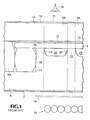
- U.S. Patent 5,077,553 discloses apparatus for addressing data storage elements. A practical implementation of the apparatus shown in U.S. Patent 5,077,553 is illustrated schematically in FIG. 1 of the accompanying drawings.
- the display panel shown in FIG. 1 comprises, in sequence from below, a polarizer 2, a channel member 4, a cover sheet 6 (commonly known as a microsheet), a layer 10 of electro-optic material, an array of parallel transparent data drive electrodes (only one of which, designated 12, can be seen in the view shown in FIG. 1), an upper substrate 14 carrying the data drive electrodes, and an upper polarizer 16.
- the panel includes color filters (not shown) between the layer 10 and the upper substrate 14.
- the panel may also include layers for improving viewing angle and for other purposes.
- the channel member 4 is typically made of glass and is formed with multiple parallel channels 20 in its upper main face.
- the channels 20, which are separated by ribs 22, are filled with an ionizable gas, such as helium.
- An anode 24 and a cathode 26 are provided in each of the channels 20.
- the channels 20 are orthogonal to the data drive electrodes and the region where a data drive electrode crosses a channel (when viewed perpendicularly to the panel) forms a discrete panel element 28.
- Each panel element can be considered to include elements of the layer 10 and the lower and upper polarizers 2 and 16.
- the region of the upper surface of the display panel that bounds the panel element constitutes a single pixel 30 of the display panel.
- the gas in the channel forms a plasma which provides a conductive path to the reference potential at the lower surface of the cover sheet 6. If a data drive electrode is at the reference potential, there is no significant electric field in the volume element of electro-optic material in the panel element at the crossing of the channel and the data drive electrode and the panel element is considered to be off, whereas if the data drive electrode is at a substantially different potential from the reference potential, there is a substantial electric field in that volume element of electro-optic material and the panel element is considered to be on.
- the lower polarizer 2 is a linear polarizer and that its plane of polarization can be arbitrarily designated as being at 0° relative to a reference plane
- the upper polarizer 16 is a linear polarizer having its plane of polarization at 90°
- the electro-optic material is a twisted nematic liquid crystal material which rotates the plane of polarization of linearly polarized light passing therethrough by an angle which is a function of the electric field in the liquid crystal material.
- the angle of rotation is 90°; and when the panel element is on, the angle of rotation is zero.
- the panel is illuminated from the underside by an extended light source 34 which emits unpolarized white light.
- a rear glass diffuser 18 having a scattering surface may be positioned between the light source and the panel in order to provide uniform illumination of the panel.
- the light that enters a given panel element from the source is linearly polarized at 0° by the lower polarizer 2 and passes sequentially through the channel member 4, the channel 20, the cover sheet 6, and the volume element of the liquid crystal material toward the upper polarizer 16 and a viewer 32. If the panel element is off, the plane of polarization of linearly polarized light passing through the volume element of liquid crystal material is rotated through 90°, and therefore the plane of polarization of light incident on the upper polarizer element is at 90°.
- the light is passed by the upper polarizer element and the pixel is illuminated. If, on the other hand, the panel element is on, the plane of polarization of the linearly polarized light is not changed on passing through the volume element of liquid crystal material. The plane of polarization of light incident on the upper polarizer element is at 0° and therefore the light is blocked by the upper polarizer element and the pixel is dark. If the electric field in the volume element of liquid crystal material is intermediate the values associated with the panel element being off and on, light is passed by the upper polarizer element with an intensity which depends on the electric field, allowing a gray scale to be displayed.
- the channel member 4 is etched back around the area in which the channels are formed in order to provide a plateau 36 in which the channels 20 are formed, and the cover sheet 6 is secured to the channel member by an endless frit bead 38 in a rabbet 40 extending around the periphery of the plateau.
- An upper substrate assembly including the upper substrate 14 and the data drive electrodes 12 carried thereby, is attached to the channel member 4 by means of a glue bead 42.
- LC materials contain free ions. These free ions can affect the optical response of a panel element to the voltage applied to the data drive electrode. In order to minimize the effect of the free ions, it is conventional to reverse the polarity of the voltages applied to the data drive electrodes at a fixed frequency. In the case of a television display, for example, this frequency is 60 Hz. on alternate frames of the image. Thus, if the potential difference between a data drive electrode and the voltage reference V ref required to achieve a particular optical state is Vd, the effect of the free ions can be reduced by driving the data drive electrode to the voltage V ref +V d on an odd frame and to the voltage V ref -V d on an even frame.
- the PALC display panel disclosed in U.S. Patent 5,077,553 is used as a raster scan display panel for displaying a raster scan video signal
- the panel is oriented so that the channels extend horizontally and the data drive electrodes extend vertically.
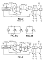
- the raster scan video signal VIDEO in which may be in accordance with a video standard such as NTSC, is supplied to a video processor 50 which generates a modified video signal VIDEO mod having suitable voltage levels for operation of the PALC display panel.
- the video processor also generates a frame switching signal FR, which changes state on consecutive frames of the video signal VIDEO mod , and a line clock signal LC.
- the modified video signal VIDEO mod is supplied both to an inverter 52 and to a non-inverting buffer 54.
- a multiplexer 56 is controlled by the frame switching signal and selects the output of the buffer 54 on odd frames and the output of the inverter 52 on even frames.
- the output signal VIDEO out of the multiplexer is supplied to a data drive electrode driver 58.
- the voltage signal V d at the output of the buffer 58 during the first active line of a frame of the video signal is supplied to a line store 60 having one storage element 62 associated with each data drive electrode 12, and each storage element stores the voltage to be applied to the associated data drive electrode during the first active line.
- the storage elements 62 are connected to the respectively associated data drive electrodes 12 by switches 60, which are closed in response to the line clock signal LC, and the data drive electrodes 12 are driven to voltage levels ⁇ V d ⁇ that depend on the respective voltages stored in the storage elements.
- a negative-going strobe pulse is applied to the cathode in the first channel to establish a plasma in the first channel.
- an electric field that establishes the optical state of the panel element is created between the data drive electrode and the lower surface of the cover sheet.
- the strobe pulse is removed, and the plasma is extinguished, but the electric field persists, maintaining the state of the panel element until the first channel is again addressed, on the next frame of the video signal. This sequence of operations is repeated in order for the remaining active lines of the frame and the remaining channels of the display panel.
- the plasma that was created in the first channel is not extinguished instantaneously when the strobe pulse is removed, but decays over a finite interval. However, it is necessary for proper operation of a plasma addressed liquid crystal display panel that the plasma created in a channel be extinguished promptly after the strobe pulse is removed.
- a plasma is considered to have decayed fully (or to be fully extinguished) if the voltage stored by the active panel element is at least 90 percent of the voltage that would have been stored if the gas in the inactive channel had not been ionized.
- the horizontal line interval can conveniently be divided into an initiation interval, during which the plasma is formed in the channel; a capture interval, during which the panel element capacitors are charged to the voltage levels of the respective data drive electrodes; and a decay interval, which starts when the strobe pulse is removed and during which the gas reverts to its non-conductive state.
- the data drive electrodes are driven to the voltage levels associated with line N+1 of the video signal between the end of the decay interval of line N and the end of the initiation interval of line N+1, so that the change in voltage levels does not affect the panel element capacitors of line N but the data drive electrodes are at the proper levels before the start of the capture interval for line N+1.
- Helium is an advantageous choice for the ionizable gas in a plasma addressed liquid crystal display panel because it is inert and therefore does not react with the electrodes in the plasma channels. Also, helium is a favorable choice with respect to sputtering damage because the helium ions are light. However, helium is not without disadvantages as the ionizable gas in a PALC panel.
- the helium atom When a helium ion recombines with an electron to form a neutral helium atom, the helium atom may be in an excited state.
- the helium atom in the excited neutral state does not always pass directly to the ground state, but it may lose a small amount of energy radiatively and pass instead to an excited metastable state.
- the excited metastable helium atoms cannot decay radiatively through dipole transitions.
- One mechanism by which excited metastable helium atoms decay is by colliding with one another to produce a helium ion-electron pair and a neutral helium atom in the ground state. This secondary ionization delays complete extinction of the plasma.
- metastable helium atom in a PALC display panel decays is through collision with the walls of the channel.
- the dimensions of the channels are such that metastable helium atoms will collide with the walls of the channel and revert to the ground state at a sufficient rate that the plasma will be considered to be fully extinguished within 30 ⁇ s after removal of the strobe pulse. Accordingly, the existence of the metastable state does not significantly degrade operation of a plasma addressed liquid crystal display panel when driven by an NTSC signal.
- the PALC display panel is to be used to provide a high addressability display, such as an HDTV display
- the number of lines of the display and the frequency at which the frame is refreshed are such that the plasma in a given channel must be reliably extinguished within about 8-16 ⁇ s after the strobe pulse is removed from the cathode.
- helium alone is used as the ionizable gas, the existence and persistence of the metastable helium atoms impairs the viewability of the display.
- a sheath layer of electrons is formed on the dielectric surfaces bounding the plasma channel. This causes the underside of the cover sheet to be at a small negative potential with respect to ground. This plasma potential applies a DC offset to the otherwise AC drive signal.
- a method of operating a PALC panel having a data drive electrode and a plasma channel comprising receiving a video signal and generating a nominal drive voltage V1 to be applied to the data drive electrode on a first frame of the video signal and a nominal drive voltage V2 to be applied to the data drive electrode on a second frame of the video signal, applying an adjusted drive voltage (V1 + V offset ) to the data drive electrode during the first frame, and applying an adjusted drive voltage (-V2 + V offset ) to the data drive electrode during the second frame.
- a method of operating a PALC panel having a data drive electrode and a plasma channel comprising receiving a video signal according to which a nominal drive voltage V1 should be applied to the data drive electrode on a first frame of the video signal and a nominal drive voltage V2 should be applied to the data drive electrode on a second frame of the video signal, applying an adjusted drive voltage (V1 + V offset ) to the data drive electrode during the first frame, and applying an adjusted drive voltage (-V2 + V offset ) to the data drive electrode during the second frame.
- a PALC panel having a plurality of data drive electrodes, a plasma channel and a drive circuit for driving the data drive electrodes in response to a video signal according to which a nominal drive voltage V1 should be applied to a given data drive electrode on a first frame of the video signal and a nominal drive voltage V2 should be applied to the given data drive electrode on a second frame of the video signal, wherein the drive circuit generates an adjusted drive voltage (V1 + V offset ) for application to the given data drive electrode during the first frame, and generates an adjusted drive voltage (-V2 + V offset ) for application to the given data drive electrode during the second frame.
- V p is the plasma potential
- ⁇ o is a time constant associated with the initial conductivity of the plasma and is typically 10 -9 -10 -7 s.
- the time constant ⁇ d2 depends on the resistance of the plasma and the capacitance of the liquid crystal and cover sheet and is typically 0.5*10 -6 - 5*10 -6 .
- the DC offset voltage V offset is essentially independent of the data voltage and can therefore be eliminated by the addition of a small DC bias to the AC drive signal.
- the output of the multiplexer 56 supplies the signal to a first input of a summing element 64 which receives the voltage V offset at a second input and generates the signal VIDEO out + V offset .
- the signal VIDEO out + V offset is supplied to the data drive electrode driver 58.
Landscapes
- Physics & Mathematics (AREA)
- Engineering & Computer Science (AREA)
- Chemical & Material Sciences (AREA)
- Crystallography & Structural Chemistry (AREA)
- Nonlinear Science (AREA)
- General Physics & Mathematics (AREA)
- Optics & Photonics (AREA)
- Mathematical Physics (AREA)
- Plasma & Fusion (AREA)
- Computer Hardware Design (AREA)
- Theoretical Computer Science (AREA)
- Control Of Indicators Other Than Cathode Ray Tubes (AREA)
- Liquid Crystal (AREA)
- Liquid Crystal Display Device Control (AREA)
Applications Claiming Priority (2)
| Application Number | Priority Date | Filing Date | Title |
|---|---|---|---|
| US8289698P | 1998-04-24 | 1998-04-24 | |
| US82896P | 2008-07-23 |
Publications (1)
| Publication Number | Publication Date |
|---|---|
| EP0952570A1 true EP0952570A1 (de) | 1999-10-27 |
Family
ID=22174150
Family Applications (1)
| Application Number | Title | Priority Date | Filing Date |
|---|---|---|---|
| EP99302868A Withdrawn EP0952570A1 (de) | 1998-04-24 | 1999-04-13 | Methode zur Ansteuerung einer plasma-adressierten Flüssigkristallanzeige zur Kompensation der Plasma -Spannung |
Country Status (4)
| Country | Link |
|---|---|
| EP (1) | EP0952570A1 (de) |
| JP (1) | JPH11338442A (de) |
| KR (1) | KR19990083435A (de) |
| CA (1) | CA2269563A1 (de) |
Families Citing this family (1)
| Publication number | Priority date | Publication date | Assignee | Title |
|---|---|---|---|---|
| KR101027770B1 (ko) * | 2009-06-02 | 2011-04-07 | 크로바하이텍(주) | 표시 장치의 데이터 드라이버 및 그 구동방법 |
Citations (1)
| Publication number | Priority date | Publication date | Assignee | Title |
|---|---|---|---|---|
| WO1997044774A2 (en) * | 1996-05-17 | 1997-11-27 | Philips Electronics N.V. | Active matrix liquid crystal display device |
-
1999
- 1999-04-13 EP EP99302868A patent/EP0952570A1/de not_active Withdrawn
- 1999-04-20 CA CA002269563A patent/CA2269563A1/en not_active Abandoned
- 1999-04-21 JP JP11113550A patent/JPH11338442A/ja active Pending
- 1999-04-23 KR KR1019990014596A patent/KR19990083435A/ko not_active Withdrawn
Patent Citations (1)
| Publication number | Priority date | Publication date | Assignee | Title |
|---|---|---|---|---|
| WO1997044774A2 (en) * | 1996-05-17 | 1997-11-27 | Philips Electronics N.V. | Active matrix liquid crystal display device |
Also Published As
| Publication number | Publication date |
|---|---|
| KR19990083435A (ko) | 1999-11-25 |
| CA2269563A1 (en) | 1999-10-24 |
| JPH11338442A (ja) | 1999-12-10 |
Similar Documents
| Publication | Publication Date | Title |
|---|---|---|
| JP3013470B2 (ja) | 画像表示装置 | |
| US5349454A (en) | Plasma addressing electro-optical device having invertor circuit connected to anodes | |
| KR100340972B1 (ko) | 플라즈마어드레스표시장치 | |
| JP2847666B2 (ja) | 電気光学表示方法 | |
| KR19980070418A (ko) | 플라즈마 어드레스 전기 광학 표시 장치 및그 구동 방법 | |
| KR950003381B1 (ko) | 플라즈마 어드레스방식의 액정표시장치 및 그 구동방법 | |
| KR100239810B1 (ko) | 화상표시장치 | |
| JP2782412B2 (ja) | プラズマ・アドレス表示装置 | |
| JP2747902B2 (ja) | アドレス指定方法及び装置 | |
| JPH1062762A (ja) | プラズマアドレス液晶表示装置 | |
| US6411030B1 (en) | Plasma display with discharge medium containing hydrogen or a hydrogen isotope | |
| CA2061384C (en) | Electro-optical device | |
| JPH11338442A (ja) | プラズマ・アドレス液晶パネル及びその動作方法 | |
| JPH08313883A (ja) | プラズマアドレス表示パネル | |
| EP0780874A2 (de) | Adressierungsstruktur unter Verwendung von ionisierungsfähigen Gasmischungen der mehrere ionisierungsfähigen Komponenten aufweisen | |
| JP2805584B2 (ja) | プラズマ・アドレス表示装置 | |
| JP3104706B1 (ja) | 画像表示装置 | |
| JP3094480B2 (ja) | 画像表示装置 | |
| JPH10171414A (ja) | 画像表示装置の初期エージング方法 | |
| KR940009147B1 (ko) | 플라즈마 어드레스 방식의 액정표시소자 | |
| JPH11194328A (ja) | プラズマ・アドレス液晶パネル動作方法 | |
| US6400345B1 (en) | Method of operating a plasma addressed liquid crystal (PALC) panel | |
| JP2002215116A (ja) | 液晶表示装置及びその駆動方法 | |
| JPH10186338A (ja) | プラズマ・アドレス液晶表示パネル用チャンネル構体及びサブアッセンブリ | |
| US20020044108A1 (en) | Plasma addressed liquid crystal display device |
Legal Events
| Date | Code | Title | Description |
|---|---|---|---|
| PUAI | Public reference made under article 153(3) epc to a published international application that has entered the european phase |
Free format text: ORIGINAL CODE: 0009012 |
|
| AK | Designated contracting states |
Kind code of ref document: A1 Designated state(s): DE FR GB NL |
|
| AX | Request for extension of the european patent |
Free format text: AL;LT;LV;MK;RO;SI |
|
| 17P | Request for examination filed |
Effective date: 20000419 |
|
| AKX | Designation fees paid |
Free format text: DE FR GB NL |
|
| STAA | Information on the status of an ep patent application or granted ep patent |
Free format text: STATUS: THE APPLICATION IS DEEMED TO BE WITHDRAWN |
|
| 18D | Application deemed to be withdrawn |
Effective date: 20021101 |