EP0952618A1 - Piezoelektrische dünnschichtanordnung, verfahren zur herstellung derselben, und schaltungselement - Google Patents
Piezoelektrische dünnschichtanordnung, verfahren zur herstellung derselben, und schaltungselement Download PDFInfo
- Publication number
- EP0952618A1 EP0952618A1 EP97919687A EP97919687A EP0952618A1 EP 0952618 A1 EP0952618 A1 EP 0952618A1 EP 97919687 A EP97919687 A EP 97919687A EP 97919687 A EP97919687 A EP 97919687A EP 0952618 A1 EP0952618 A1 EP 0952618A1
- Authority
- EP
- European Patent Office
- Prior art keywords
- acoustic wave
- wave device
- wafer
- film
- film acoustic
- Prior art date
- Legal status (The legal status is an assumption and is not a legal conclusion. Google has not performed a legal analysis and makes no representation as to the accuracy of the status listed.)
- Withdrawn
Links
Images











Classifications
-
- H—ELECTRICITY
- H10—SEMICONDUCTOR DEVICES; ELECTRIC SOLID-STATE DEVICES NOT OTHERWISE PROVIDED FOR
- H10N—ELECTRIC SOLID-STATE DEVICES NOT OTHERWISE PROVIDED FOR
- H10N30/00—Piezoelectric or electrostrictive devices
- H10N30/20—Piezoelectric or electrostrictive devices with electrical input and mechanical output, e.g. functioning as actuators or vibrators
-
- H—ELECTRICITY
- H03—ELECTRONIC CIRCUITRY
- H03H—IMPEDANCE NETWORKS, e.g. RESONANT CIRCUITS; RESONATORS
- H03H9/00—Networks comprising electromechanical or electro-acoustic elements; Electromechanical resonators
- H03H9/46—Filters
- H03H9/54—Filters comprising resonators of piezoelectric or electrostrictive material
- H03H9/56—Monolithic crystal filters
- H03H9/564—Monolithic crystal filters implemented with thin-film techniques
-
- H—ELECTRICITY
- H03—ELECTRONIC CIRCUITRY
- H03H—IMPEDANCE NETWORKS, e.g. RESONANT CIRCUITS; RESONATORS
- H03H3/00—Apparatus or processes specially adapted for the manufacture of impedance networks, resonating circuits, resonators
- H03H3/007—Apparatus or processes specially adapted for the manufacture of impedance networks, resonating circuits, resonators for the manufacture of electromechanical resonators or networks
- H03H3/02—Apparatus or processes specially adapted for the manufacture of impedance networks, resonating circuits, resonators for the manufacture of electromechanical resonators or networks for the manufacture of piezoelectric or electrostrictive resonators or networks
- H03H3/04—Apparatus or processes specially adapted for the manufacture of impedance networks, resonating circuits, resonators for the manufacture of electromechanical resonators or networks for the manufacture of piezoelectric or electrostrictive resonators or networks for obtaining desired frequency or temperature coefficient
-
- H—ELECTRICITY
- H03—ELECTRONIC CIRCUITRY
- H03H—IMPEDANCE NETWORKS, e.g. RESONANT CIRCUITS; RESONATORS
- H03H9/00—Networks comprising electromechanical or electro-acoustic elements; Electromechanical resonators
- H03H9/02—Details
- H03H9/05—Holders or supports
- H03H9/0538—Constructional combinations of supports or holders with electromechanical or other electronic elements
- H03H9/0542—Constructional combinations of supports or holders with electromechanical or other electronic elements consisting of a lateral arrangement
-
- H—ELECTRICITY
- H03—ELECTRONIC CIRCUITRY
- H03H—IMPEDANCE NETWORKS, e.g. RESONANT CIRCUITS; RESONATORS
- H03H9/00—Networks comprising electromechanical or electro-acoustic elements; Electromechanical resonators
- H03H9/15—Constructional features of resonators consisting of piezoelectric or electrostrictive material
- H03H9/17—Constructional features of resonators consisting of piezoelectric or electrostrictive material having a single resonator
- H03H9/171—Constructional features of resonators consisting of piezoelectric or electrostrictive material having a single resonator implemented with thin-film techniques, i.e. of the film bulk acoustic resonator [FBAR] type
- H03H9/172—Means for mounting on a substrate, i.e. means constituting the material interface confining the waves to a volume
- H03H9/173—Air-gaps
-
- H—ELECTRICITY
- H03—ELECTRONIC CIRCUITRY
- H03H—IMPEDANCE NETWORKS, e.g. RESONANT CIRCUITS; RESONATORS
- H03H9/00—Networks comprising electromechanical or electro-acoustic elements; Electromechanical resonators
- H03H9/15—Constructional features of resonators consisting of piezoelectric or electrostrictive material
- H03H9/17—Constructional features of resonators consisting of piezoelectric or electrostrictive material having a single resonator
- H03H9/171—Constructional features of resonators consisting of piezoelectric or electrostrictive material having a single resonator implemented with thin-film techniques, i.e. of the film bulk acoustic resonator [FBAR] type
- H03H9/172—Means for mounting on a substrate, i.e. means constituting the material interface confining the waves to a volume
- H03H9/174—Membranes
-
- H—ELECTRICITY
- H03—ELECTRONIC CIRCUITRY
- H03H—IMPEDANCE NETWORKS, e.g. RESONANT CIRCUITS; RESONATORS
- H03H9/00—Networks comprising electromechanical or electro-acoustic elements; Electromechanical resonators
- H03H9/15—Constructional features of resonators consisting of piezoelectric or electrostrictive material
- H03H9/17—Constructional features of resonators consisting of piezoelectric or electrostrictive material having a single resonator
- H03H9/176—Constructional features of resonators consisting of piezoelectric or electrostrictive material having a single resonator consisting of ceramic material
-
- H—ELECTRICITY
- H03—ELECTRONIC CIRCUITRY
- H03H—IMPEDANCE NETWORKS, e.g. RESONANT CIRCUITS; RESONATORS
- H03H9/00—Networks comprising electromechanical or electro-acoustic elements; Electromechanical resonators
- H03H9/46—Filters
- H03H9/54—Filters comprising resonators of piezoelectric or electrostrictive material
- H03H9/56—Monolithic crystal filters
- H03H9/562—Monolithic crystal filters comprising a ceramic piezoelectric layer
-
- Y—GENERAL TAGGING OF NEW TECHNOLOGICAL DEVELOPMENTS; GENERAL TAGGING OF CROSS-SECTIONAL TECHNOLOGIES SPANNING OVER SEVERAL SECTIONS OF THE IPC; TECHNICAL SUBJECTS COVERED BY FORMER USPC CROSS-REFERENCE ART COLLECTIONS [XRACs] AND DIGESTS
- Y10—TECHNICAL SUBJECTS COVERED BY FORMER USPC
- Y10T—TECHNICAL SUBJECTS COVERED BY FORMER US CLASSIFICATION
- Y10T29/00—Metal working
- Y10T29/42—Piezoelectric device making
Definitions
- the invention relates to a film acoustic wave device such as filter and resonator that utilizes acoustic waves, and a manufacturing method of the film acoustic wave device.
- the film acoustic wave device Using a conversion process from electric signals to acoustic waves for a piezoelectric material, the film acoustic wave device functions as a filter or a resonator.
- Figs.34, 35, 36 and 37 are examples of conventional film acoustic wave devices of this type as disclosed in the Japanese examined patent publication "sho61-269410" (hereinafter document 1).
- Fig.34 is a configuration of the conventional bulk acoustic wave device of this type.
- Fig.35 is a cross-section cut through A-A of Fig.34.
- a glass substrate 1 a piezoelectric thin film 2 made of zinc oxide (ZnO); an interdigital transducer of input side 3; and an interdigital transducer of output side 4; electrode fingers 5; and opposing electrodes 6 made of aluminum (Al).
- ZnO zinc oxide
- electrode fingers 5 electrode fingers 5; and opposing electrodes 6 made of aluminum (Al).
- Figs.36 and 37 are graphs that show properties of this type of conventional film acoustic wave device of Figs.34 and 35.
- Fig.36 shows a relationship between an acoustic velocity Vs and a normalized thickness of thin film kh.
- Fig.37 shows a relationship of an electromechanical coupling constant K 2 and the normalized thickness of thin film.
- Figs.38 is a cross-section similar to Fig.35.
- Fig.39 shows a relationship between the acoustic velocity Vs and the normalized thickness of thin film for the conventional film acoustic wave device of Fig.38.
- Fig.40 shows a relationship of the electromechanical coupling constant K 2 and the normalized thickness of thin film.
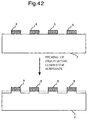
- Figs.41 and 42 are examples of the conventional acoustic wave devices of this type as disclosed in the Japanese unexamined patent publication "hei2-189011" (hereinafter document 3).
- the electrode fingers 5 are placed on top of the glass substrate 1, and then the piezoelectric thin film 2 made of ZnO is placed on top of the two.
- An electric field is formed on an intersecting part of the electrode fingers 5 from electric signals applied to the interdigital transducer of input side 3. Due to the electric field, the piezoelectric thin film 2 is stretched to excite the acoustic waves.
- the acoustic waves that have been excited at the interdigital transducers of input side 3 propagates in a direction parallel to a surface, and reaches the interdigital transducers of output side 4 accompanied by the electric field and the acoustic vibrations.
- the electrode fingers 5 again receive the electric field which is formed by the acoustic waves, and change the electric field back to the electric signal. Since a reverse conversion of electric signals and acoustic waves is possible, the process of reverse conversion of the electric field made by the acoustic waves back to the electric signals is considered same as the case of the interdigital transducers of input side 3.
- acoustic waves which propagate in the direction parallel to the surface due to a concentration of energy at the surface
- bulk waves which propagate in the direction parallel to the surface
- the bulk waves which propagates in a direction of thickness.
- intensities of acoustic wave excitations are determined by materials being used, combination of the materials, the physical dimensions such as thickness of each material, as well as the configuration of electrodes that excites the acoustic waves.
- the film acoustic wave device of Fig.35 uses the surface acoustic waves.
- the configuration of electrode fingers 5 as shown in Figs.34 and 35 are commonly being used to excite the surface acoustic waves.
- An efficiency of conversion from the electric signals which are applied to the interdigital transducers of input side 3 to the surface acoustic waves relates largely on a performance of the film acoustic wave device, and as one of a figure of merit that indicates the conversion efficiency, there is electromechanical coupling constant K 2 .
- the larger the electromechanical coupling constant K 2 for example, the filters that are less damaging and having wide-ranging properties become possible.
- the electromechanical coupling constant K 2 is determined by the materials being used, the combination of the materials, the physical dimensions such as the thickness of each material, and the configuration of electrode that excites the acoustic waves.
- Fig.36 and 37 illustrate the properties of the film acoustic wave devices with this configuration, as described in the document 1.
- Fig.36 is a graph that shows a relationship between the acoustic velocity Vs and the normalized thickness of thin film kh.
- Fig.37 is a graph that shows a relationship between the electromechanical coupling constant K 2 and the normalized thickness of thin film kh.
- h refers to a thickness of piezoelectric thin film 2
- k refers to a wave number of the surface acoustic waves that propagate in the direction parallel to the surface.
- the normalized thickness of thin film kh is a multiple of the wave number k and the thickness h.
- the wave number k is (2 ⁇ / ⁇ ) or (2 ⁇ f/Vs)
- the wave number k is also a fixed number that the normalized thickness kh on a horizontal axis is possible to be substituted with the thickness h.
- Fig.36 is indicating a relationship of the acoustic velocity Vs and the thickness h of piezoelectric thin film 2, and even when the thickness h changes, the acoustic velocity Vs is fixed.
- Fig.37 is showing the relationship of the thickness h of piezoelectric thin film 2 and the electromechanical coupling constant K 2 , and in a range of kh from 3 to 4, the electromechanical coupling constant K 2 is close to a maximum, indicating that it is also fixed.
- the acoustic velocity Vs and the electromechanical coupling constant K 2 for the film acoustic wave devices are almost fixed.
- the acoustic velocity Vs relates to a center frequency of the film acoustic wave device, and the electromechanical coupling constant K 2 largely relates to an insertion loss of the film acoustic wave device.
- the range of normalized thickness of the thin films kh is from 3 to 4 as in Figs.36 and 37, and the center frequency and the insertion loss of film acoustic wave device is approximately a fixed number.
- Fig.38 is showing the conventional film acoustic wave device of this type as in the document 2, and is a cross-sectional view similar to Fig.35.
- the glass substrate 1 the piezoelectric thin film 2 made of ZnO or aluminum nitride (AlN), and the electrode fingers 5 that make up the interdigital transducers.
- the conventional film acoustic wave device of this type shown in Fig.38 is using the surface acoustic waves.
- the configuration resembles the configuration shown in Fig.35 where the electrode fingers 5 are placed on top of the glass substrate 1, and then place the piezoelectric thin film 2 on top of the two.
- the opposing electrodes 6 are not placed on top of the piezoelectric thin film 2.
- Fig.39 shows a relationship of the normalized thickness of thin film kh and the acoustic velocity Vs.
- Fig.40 shows a relationship of the normalized thickness of thin film kh and the electromechanical coupling constant K 2 .
- a reason for the film acoustic wave device illustrated in Fig.38 being so different in properties from Figs.36 and 37 is the non-metallic surface of the piezoelectric thin film 2.
- a case illustrated in Fig.39 is different from the case illustrated in Fig.36, where the acoustic velocity Vs changes when the normalized thickness of thin film kh changed.
- the electromechanical coupling constant K 2 becomes greater than 2.
- the center frequency of film acoustic wave device is adjusted by directly changing the thickness h of piezoelectric thin film 2.
- methods of adjusting the thickness h of piezoelectric thin film 2 illustrates the use of a sputter to make a thicker film and a use of etching method to make a thinner film. As long as the configuration is like those illustrated in Fig.38, there will be no effect on the electrode fingers 5 by changing the thickness of piezoelectric thin film 2 using the etching or sputtering methods.
- Figs.41 and 42 illustrate the conventional acoustic wave devices of this type as disclosed in document 3.
- the piezoelectric substrate 7 is used instead of the piezoelectric thin film 2.
- a numeral 5 is indicating the electrode fingers 5.
- the conventional acoustic wave device of the type shown in Fig.41 is the surface acoustic wave device used by exciting the surface acoustic waves by the electrode fingers 5.
- the velocity of surface acoustic waves that propagate through the electrode fingers 5 is known to have a different acoustic velocity from the acoustic velocity at a region where there is no electrode fingers 5, and this is due to effects of a mass load and an electrical boundary condition of the electrode fingers 5.
- the surface acoustic wave device of Fig.41 by changing the thickness of electrode fingers 5 by etching the electrode material, the acoustic velocity is changed by the mass load effect, and then the center frequency of the surface acoustic wave device is adjusted.
- Standard processes of forming the piezoelectric thin film 2 and the metal electrode are the sputtering and a vacuum evaporation.
- these methods of forming the films looking from a target 8 of the sputter and vacuum evaporation, at a central portion of wafer the resulting film becomes relatively thick, and at periphery of the wafer the resulting film becomes relatively thin.
- the target 8 and the wafer 9 where the film components land are arranged one-to-one inside a vacuum container 10
- the formation of film in the central portion of wafer 9 is thick of h c and in the periphery of wafer 9 is thin of h e , as shown in Fig.44. Therefore, in this type of film acoustic wave device, the adjustment of frequency was needed to overcome the variation in the thickness of piezoelectric thin film and film formed on the metal electrode.
- center frequencies are adjusted by changing the thickness of piezoelectric substrate 7 partially, the thickness of piezoelectric thin film 2 and the electrode fingers 5.
- a plurality of these devices are arranged on top of the wafer made of a single plate of glass substrate or the piezoelectric substrate 7, and the plurality of these devices are manufactured at once. From this, when need to partially change the thickness of piezoelectric thin film 2, the thickness of electrode fingers 5, and the thickness of piezoelectric conductor 7, the thickness are adjusted in a wafer unit or adjusted after separating the individual devices from each other for adjustment of every one of the devices.
- the films formed on top of the wafer 9 is thick at central portion and thin in its periphery.
- a problem in the conventional film acoustic wave device was that the adjustment was not possible.
- the invention in attempt to solve the problem, aims to provide a film acoustic wave device and a manufacturing method of film acoustic wave device that can adjust a variation of thickness inside the wafer, without increasing the manufacturing cost.
- a film acoustic wave device comprises a wafer made of a semiconductor substrate, a ground electrode formed on top of the semiconductor substrate, a piezoelectric thin film formed on top of the ground electrode, and an upper electrode formed on top of the piezoelectric thin film.
- a pattern shape for the film acoustic wave device is changed by a position at the wafer.
- a length of the upper electrode of the film acoustic wave device is changed by the position at the wafer.
- a width of the upper electrode of the film acoustic wave device is changed by the position at the wafer.
- the upper electrode of the film acoustic wave device includes a plurality of upper electrodes, and distances between the upper electrodes are changed by the position at the wafer.
- the film acoustic wave device further comprises a bonding pad for connecting with the upper electrode.
- a shape of the bonding pad is changed by the position at the wafer.
- the film acoustic wave device further comprises a connecting pattern for connecting the upper electrode with the bonding pad.
- a shape of the connecting pattern is changed by the position at the wafer.
- the connecting pattern of the film acoustic wave device forms an air bridge.
- the film acoustic wave device further comprises a capacitor provided on the same semiconductor substrate as the film acoustic wave device. A capacity of the condenser is changed by the position of the wafer.
- the film acoustic wave device includes the followings: semiconductor substrate made of gallium arsenide (GaAs); the piezoelectric thin film made of lead titanate (PbTiO 3 ); and at least one of the upper electrodes and ground electrode which is a conductor substantially made of platinum (Pt).
- the film acoustic wave device includes the followings: a semiconductor substrate made of silicon (Si); the piezoelectric thin film made of lead titanate (PbTiO 3 ); and at least one of the upper electrode and ground electrode which is a conductor substantially made of platinum (Pt).
- the film acoustic wave device includes the followings: the piezoelectric thin film made of PZT (PbTiO 3 -PbZrO 3 ); and at least one of the upper electrode and the ground electrode which is a conductor substantially made of platinum (Pt).
- the piezoelectric thin film of the film acoustic wave device is made of zinc oxide (ZnO).
- the piezoelectric thin film of the film acoustic wave device is made of aluminum nitride (AlN).
- the film acoustic wave device further comprises an inductor between the semiconductor substrate and the ground electrode.
- a circuit device comprises a substrate, and a plurality of elements formed on the substrate.
- the pattern shape of the elements formed on the substrate is changed by a position at the substrate.
- a manufacturing method of the film acoustic wave device comprises of the following steps:
- the manufacturing method of the film acoustic wave device includes the step of changing the pattern shape.
- the step includes a step of changing the length of the upper electrode by the position at the wafer.
- the manufacturing method of the film acoustic wave device includes the step of changing the pattern shape.
- the step includes a step of changing the width of the upper electrode by the position at the wafer.
- the manufacturing method of the film acoustic wave device includes the step of forming the upper electrode which forms a plurality of upper electrodes.
- the step of changing the pattern shape includes a step of changing the distance between the upper electrodes by the position at the wafer.
- the manufacturing method of the film acoustic wave device includes the step of forming the upper electrode. This step further includes a step of connecting of the upper electrode to a bonding pad. As well, the manufacturing method of the film acoustic wave device includes step of changing the pattern shape. This step further includes a step of changing a shape of the bonding pad by the position at the wafer.
- the manufacturing method of the film acoustic wave device includes the step of forming the upper electrode. This step further includes the connecting the upper electrode and the bonding pad to a connecting pattern. As well, the manufacturing method of the film acoustic wave device includes the step of changing the pattern shape. This step further includes a step of changing a shape of the connecting pattern by the position at the wafer.
- the manufacturing method of the film acoustic wave device includes the step of changing the pattern shape which further includes a step of forming the connecting pattern with the air bridge.
- the manufacturing method of the film acoustic wave device further comprises a step for setting a capacitor on the same semiconductor substrate as the film acoustic wave device.
- the step of changing the pattern shape further includes a step of changing a capacity of the condenser by the position at the wafer.
- Fig.1 illustrates the film acoustic wave devices for embodiment 1.
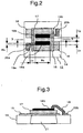
- Fig.2 is an enlarged diagram of the film acoustic wave device shown in Fig.1.
- Fig.3 is a cross-section B-B of Fig.2.
- a wafer 11 is a semiconductor made of gallium arsenide (GaAs); film acoustic wave devices 12a ⁇ 12c formed on top of the wafer 11; an orientation flat 13 showing the standard surface of the wafer 11; a semiconductor substrate 14 made of gallium arsenide (GaAs); a ground electrode 15; bonding pads 16 at same electric potential as the ground electrode 15; a piezoelectric thin film 17 made of lead titanate (PbTiO 3 ); upper electrodes 18a and 18b; connecting patterns 19a and 19b; bonding pads 20a and 20b respectively connected to the upper electrodes 18a and 18b; and a via hole 21.
- a film acoustic wave device 12 shown in Fig.2 is a filter made of a single upper electrode of input side 18a and a single upper electrode of output side 18b.
- This filter uses bulk waves, unlike the surface acoustic wave filter. That is, the filter uses the resonance of thickness direction and resonance between the upper electrode of input side 18a and upper electrode of output side 18b, using a fewer number of electrodes than the surface acoustic wave filters.
- the filter has the following pattern dimensions: length of upper electrodes 18a and 18b is Le; width is We; and distance between the upper electrode of input side 18a and upper electrode of output side 18b is La. Length of connecting patterns 19a and 19b is Lg and width is Wa.
- the Fig.3 shows a use of air bridge to the connecting patterns 19a and 19b.
- the measurements of each pattern Le, We, Lg, La and Wa determines the frequency response of the film acoustic wave device 12 as well as the thickness h of piezoelectric thin film 17.
- a plurality of film acoustic wave devices 12a ⁇ 12c are arranged on top of a single wafer 11.
- 100 or more of film acoustic wave devices are arranged, however, for the purpose of simplicity, Fig.1 has been simplified. Since a several number of the film acoustic wave devices 12a ⁇ 12c are arranged on top of the single wafer 11, much number of the film acoustic wave devices 12 can be manufactured at once from a processing of the single wafer 11.
- a cost of the processing of single wafer 11 does not question a number of film acoustic wave devices 12, but the cost is determined by the number of wafer processing. The greater the number of film acoustic wave devices 12 obtained from the single wafer, the cost of manufacturing per film acoustic wave device 12 becomes low.
- more than one wafer can be processed at one wafer processing which will further reduce the manufacturing cost.
- the vacuum evaporation or the sputtering are commonly used in forming the films on ground electrode 15, the piezoelectric thin film and upper electrodes 18a and 18b.
- the lower electrode 15, the piezoelectric thin film 17 and the upper electrodes 18a and 18b are formed inside a surface of the wafer 11, and all tend to have a slight variation in thickness distribution.
- the thickness distribution here is a structural change in film component. For example, when sputtering the piezoelectric thin film 17 onto a single wafer, as Fig.44 shows, a central portion of the wafer becomes thick and a periphery of the wafer becomes thin.
- the thickness distribution is also affected by a condition of the wafer at the sputtering. For instance, when rotating the wafer inside a sputtering apparatus, this may result in the thickness distribution in a form of band at a central portion of the wafer.
- a variation in the thickness of piezoelectric thin film 17 is a change in frequency upon manufacturing the film acoustic wave device 12.
- a frequency of the film acoustic wave device 12a decreases at the central part of wafer 11, and at a periphery of the wafer 11 where the piezoelectric thin film 19 becomes thinner compared to the central part of the wafer, the frequency of film acoustic wave device 12b is increases.
- the frequency at the central part and the periphery of the wafer for the film acoustic wave devices are adjusted.
- at least more than one of the pattern measurements Le, We, Lg, La and Wa are changed for the film acoustic wave device 12c in a direction perpendicular to the orientation flat 13
- the film acoustic wave device 12b in a direction parallel to the orientation flat 13.
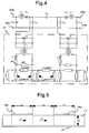
- Figs.4 to 6 are diagrams describing calculations of the frequency responses.
- Fig.4 shows the equivalent circuit of the film acoustic wave device 12 of Fig.2.
- Fig.5 is a cross-section for regions of the upper electrode of input side 18a and the upper electrode of output side 18b for the film acoustic wave device 12.
- a part enclosed in square with dashed line is the equivalent circuit 24 for a bulk acoustic wave filter.
- the equivalent circuit 24 is connected to the part corresponding to the section from the upper electrode of input side 18a to the upper electrode of output side 18b.
- the equivalent circuit 24 of the bulk acoustic wave filter is corresponding to a path of signal from the upper electrode of input side 18a to the upper electrode of output side 18b, as shown in Fig.5.
- Upper capacitors C s1 , C s2 , and C i0 , an inductor L s1 , and a resistor R s1 for the equivalent circuit 24 of bulk acoustic wave filter are stray components of the connecting patterns 19a and 19b and the bonding pads 20a and 20b for the film acoustic wave device 12.
- the capacitor C s1 represents a capacitance of the bonding pads 20a and 20b and a capacitive reactance of the connecting patterns 19a and 19b.
- the capacitor C s2 represents a capacitance of upper electrodes 18a and 18b (except for the piezoelectric thin film 17) and the capacitive reactance of the connecting patterns 19a and 19b.
- the capacitor C i0 represents a capacitance between the upper electrode of input side 18a and the upper electrode of output side 18b.
- the inductor L s1 represents an inductive reactance of the connecting patterns 19a and 19b.
- the resistor R s1 represents a resistance such as a conductor resistance of the electrodes 18a and 18b, the connecting patterns 19a and 19b, and the bonding pads 20a and 20b.
- Fig.6 is a graph showing the frequency response of the film acoustic wave device 12 calculated using the equivalent circuit of Fig.4.
- the graph shows the following frequency response: a dashed line represents a resonant frequency f o of 2.5GHz; a double dotted line represents the resonant frequency f o of 2.52GHz; a single dotted line represents the resonant frequency f o of 2.54GHz; a dotted chained line represents the resonant frequency f o of 2.56GHz; and a plain line represents the resonant frequency f o of 2.58GHz.
- a density of the piezoelectric thin film is 7700kg/m 3 , a relative dielectric constant is 200, a parallel resonance of Q which determines a resistor r s is 500, a series resonance of Q which determines a conductance g s is 500, a normalized length of electrode (Le/h) is 10, a normalized distance between electrodes (Lg/h) is 0.6, a normalized width of electrode (We/h) is 111, the thickness is approximately 0.9 ⁇ m, C s1 is 0.8pF, C s2 is 0.2pF, C io is 0.02pF, L s1 is 8nH, and R s1 is 6 ⁇ .
- An effective piezoelectric constant of electrode is 4.0C/m
- a propagation loss of acoustic wave along to a surface of the electrode is 3dB/100 ⁇ m
- a normalized cutoff frequency (f m /f o ) is 0.734
- a constant which determines a gradient of dispersion property is -14.9754
- an effective piezoelectric constant of the electrode part is 0.2C/m
- a propagation loss of acoustic wave along to a surface of the electrode is 3dB/100 ⁇ m
- the normalized cutoff frequency (f n /f o ) is 0.802
- the constant which determines gradient of dispersion property is -17.5854.
- the values are obtained from the piezoelectric thin film 17 made of lead titanate (PbTiO 3 ) and the ground electrode 15 and the upper electrodes 18a and 18b made of platinum (Pt).
- the resonant frequency f o of the thickness-extensional wave is inversely proportional to the thickness h of the piezoelectric thin film 17.
- Fig.7 illustrates the film acoustic wave device for embodiment 2.
- a description of the numbered components indicated in Fig.7 follows: the wafer 11, the film acoustic wave device 12a in a central part of the wafer; the film acoustic wave device 12b in a peripheral part of the wafer that parallels in the direction of orientation flat 13; the film acoustic wave device 12c in the peripheral part of the wafer that is perpendicular to the direction of orientation flat 13; and the upper electrode of input side 18a and the upper electrode of output side 18b.
- the distances Lg between the upper electrodes of input side 18a and output side 18b are changed for the film acoustic wave device 12a at the central wafer and the film acoustic wave devices 12b and 12c at the peripheral wafer.
- Fig.8 shows the calculated results of frequency response when the distances Lg between the electrodes are changed.
- the frequency response are calculated using the equivalent circuit of Fig.4.
- the frequency response are calculated by changing the normalized distance between the electrodes (Lg/h) from 0.4 to 0.7.
- the normalized length of electrode (Le/h) is 10, and the normalized width of electrode (We/h) is 111, and all other calculation parameters are same as in Fig.6.
- Fig.8 shows the normalized distances between the electrodes (Lg/h) are from 0.4 to 0.7, however, if the type of piezoelectric thin film 17, the thickness of piezoelectric thin film 17, the type of electrode, the thickness, the measurements and the stray components such as the element value of equivalent circuit are different from Fig.8, then an appropriate range for the normalized distance between the electrodes (Lg/h) will be different from the case shown in Fig.8.
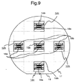
- Fig.9 illustrates the film acoustic wave device for embodiment 3.
- a description of the numbered components indicated in Fig.9 follows: the wafer 11, the film acoustic wave device 12a in a central part of the wafer; the film acoustic wave device 12b in the peripheral part of the wafer that parallels in the direction of orientation flat 13; the film acoustic wave device 12c in the peripheral part of the wafer that is perpendicular to the direction of orientation flat 13; and the upper electrode of input side 18a and the upper electrode of output side 18b.
- width We of the upper electrodes 18a and 18b are changed for the film acoustic wave device 12a of the central wafer 11 and the film acoustic wave devices 12b and 12c of the peripheral wafer 11.
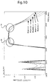
- Fig.10 shows the calculated results of the frequency response when the normalized width of electrodes (We/h) are changed.
- the frequency response are calculated by changing the normalized width of electrodes (We/h) from 111 to 66.7.
- the normalized length of electrode (Le/h) is 10
- the distance between the normalized electrodes (Lg/h) is 0.6
- all other calculation parameters are same as in Fig.6.
- the low frequency side of the passband is, it is an edge of the passband on a low frequency side that are increased by a required amount from a minimum loss value of the passband.
- the high frequency side of the passband is another edge of the passband on a high frequency side that are increased by the required amount from the minimum loss value of the passband.
- the required amount for increase from the minimum loss value is normally 3dB.
- bandwidth 3dB a difference in frequency of the passband on the high frequency side from the low frequency side.
- Fig.11 illustrates the film acoustic wave device for embodiment 4.
- FIG.11 A description of the numbered components indicated in Fig.11 follows: the wafer 11, the film acoustic wave device 12a in a central part of the wafer; the film acoustic wave device 12b in a peripheral part of the wafer that parallels in the direction of orientation flat 13; the film acoustic wave device 12c in the peripheral part of the wafer that is perpendicular to the direction of orientation flat 13; and the upper electrode of input side 18a and the upper electrode of output side 18b.
- the length Le for the upper electrodes 18a and 18b are changed for the film acoustic wave device 12a at the central wafer and the film acoustic wave devices 12b and 12c at the peripheral wafer.
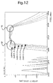
- Fig.12 shows the calculated results of the frequency response when the normalized length of electrodes (Le/h) are changed.
- the frequency response are calculated by changing the normalized length of electrodes (Le/h) from 8 to 12.
- the normalized width of electrodes (We/h) are 111, and the normalized distance between the electrodes (Lg/h) is 0.6, and all other calculation parameters are same as in Fig.6.
- Fig.13 illustrates the film acoustic wave device for embodiment 5.
- a description of the numbered components indicated in Fig.13 follows: the wafer 11, the film acoustic wave device 12a in a central part of the wafer; the film acoustic wave device 12b in a peripheral part of the wafer that parallels in the direction of orientation flat 13; the film acoustic wave device 12c in the peripheral part of the wafer that is perpendicular to the direction of orientation flat 13; and the connecting patterns 19a and 19b.
- length La of the connecting patterns 19a and 19b are changed for the film acoustic wave device 12a at the central wafer and for the film acoustic wave device 12b at the peripheral wafer.
- Width Wa of the connecting patterns 19a and 19b are also changed for the film acoustic wave device 12a at the central wafer and the film acoustic wave device 12c at the peripheral wafer.
- Fig.14 shows a result of the frequency response upon changing the inductor L s1 shown in Fig.4.
- the inductor L s1 is calculated by changing its inductance from 4nH to 12nH.
- the inductance of inductor L s1 mainly changes by changing at least one of a length La or a width Wa of connecting patterns 19a and 19b.
- the normalized width of electrode (We/h) is 77.8, and the normalized length of electrode (Le/h) is 10, and the normalized distance between the electrodes (Lg/h) is 0.6, and all other calculation parameters are same as in Fig.6.
- Fig.13 of the present embodiment is showing a case of changing both the length La and the width Wa of connecting patterns 19a and 19b, however, a case can be made to change the length La of connecting patterns 19a and 19b. Alternatively, a case to change only the width Wa of connecting patterns 19a and 19b is also possible. Furthermore, the length La and the width Wa of connecting patterns 19a and 19b can both be changed at the same time.
- Fig.15 illustrates the film acoustic wave device for embodiment 6.
- a description of the numbered components indicated in Fig.15 follows: the wafer 11, the film acoustic wave device 12a in a central part of the wafer; the film acoustic wave device 12b in a peripheral part of the wafer that parallels in the direction of orientation flat 13; the film acoustic wave device 12c in the peripheral part of the wafer that is perpendicular to the direction of orientation flat 13; the connecting patterns 19a and 19b; and the bonding pads 20a and 20b.
- Fig.16 shows a calculated result of the frequency response when the capacitor C s1 shown in Fig.4 is changed.
- the capacitor C s1 is calculated by changing its capacitance from 0.4pF to 1.2pF.
- the capacitance of capacitor C s1 mainly change by changing the followings: area of bonding pads 20a and 20b; capacitance of the capacitor electrically connected to bonding pads 20a and 20b; and the length La and the width Wa of connecting patterns 19a and 19b.
- the normalized width of electrode (We/h) is 77.8, the normalized length of electrode (Le/h) is 10, and the normalized distance between the electrodes (Lg/h) is 0.6, and all other calculation parameters are same as in Fig.6.
- the Fig.17 illustrates the film acoustic wave device for embodiment 7.
- a description of the numbered components indicated in Fig.17 follows: the wafer 11, the film acoustic wave device 12a in a central part of the wafer; the film acoustic wave device 12b in a peripheral part of the wafer that parallels in the direction of orientation flat 13; the film acoustic wave device 12c in the peripheral part of the wafer that is perpendicular to the direction of orientation flat 13; and the connecting patterns 19a and 19b.
- Fig.17 of the present embodiment length La and width Wa of the connecting patterns 19a and 19b are changed for the film acoustic wave device 12a at the central wafer, and the film acoustic wave devices 12b and 12c at the peripheral wafer. This is equivalent to changing the capacitor C s2 of Fig.4.
- Fig.18 is a calculated result of the frequency response when the capacitor C s2 shown in Fig.4 is changed.
- the capacitor C s2 is calculated by changing its capacitance from 0.1pF to 0.5pF.
- the capacitance of capacitor C s2 mainly changes by changing the length La or width Wa of connecting patterns 19a and 19b, and by changing the shape and area of upper electrodes 18a and 18b.
- the normalized width of electrode (We/h) is 77.8, the normalized length of electrode (Le/h) is 10, the normalized distance between the electrodes (Lg/h) is 0.6, and all other calculation parameters are same as in Fig.6.
- the passband of the film acoustic wave devices 12 can be controlled by changing the length Le and width We of the upper electrodes 18a and 18b, the distance Lg between the upper electrodes 18a and 18b, the length La and width Wa of the connecting patterns 19a and 19b, the areas of the bonding pads 20a and 20b, and the capacitance of capacitor connected electrically to the bonding pads 20a and 20b.
- the compensation of variation of passband for the film acoustic wave device 12 due to the thickness distribution of piezoelectric thin film 17 on top of the wafer, for instance, as Fig.1 shows, is carried out by changing the length Le and width We of the upper electrodes 18a and 18b, the distance Lg between the upper electrodes 18a and 18b, the length La and width Wa of connecting electrodes 19a and 19b, the areas of the bonding pads 20a and 20b, and the capacitance of capacitor connected electrically to the bonding pads 20a and 20b.
- Figs.19, 20 and 21 illustrate the film acoustic wave device for embodiment 8.
- the wafer 11 made of silicon (Si) conductor; the film acoustic wave devices 12a ⁇ 12c; the orientation flat 13 showing the standard surface of wafer 11; a silicon (Si) semiconductor substrate 25; the ground electrode 15; bonding pads 16 at equal electric potential as ground electric potential; the piezoelectric thin film 17 made of lead titanate (PbTiO 3 ); the upper electrodes 18a and 18b; the connecting patterns 19a and 19b; the bonding pads 20a and 20b respectively connected to the upper electrodes 18a and 18b; and the via hole 21.
- Figs.8 to 18 are showing, for the film acoustic wave devices 12a ⁇ 12c, by changing the variables of length Le and width We of upper electrodes 18a and 18b, distance Lg between the upper electrodes 18a and 18b, length La and width Wa of connecting patterns 19a and 19b, the capacitance of capacitor connected electrically to bonding pads 20a and 20b, variation of frequency response from the positioning at the wafer 11 is compensated. From this, even if thickness distribution is formed on top of the piezoelectric thin film 17 from positioning at the wafer 11, the film acoustic wave device 12 with a less variation of frequency response is obtained.
- a semiconductor substrate 14 made of gallium arsenide (GaAs) shown in Fig.1 has a good insulation, and as for a configuration of the film acoustic wave device 12 there is an advantage of minimizing a loss from the semiconductor substrate 14.
- its cost being expensive that it is disadvantaged in terms of manufacturing cost.
- a semiconductor substrate 25 made of silicon (Si) can be manufactured in massive quantity and expense for the wafer 11 is less.
- a radius of the wafer is larger, and when compare a single wafer with the semiconductor substrate 14 made of gallium arsenide (GaAs), the mass production of the film acoustic wave devices 12 is possible, and the manufacturing cost is reduced. Since the area of the wafer 11 is large, a thickness variation of piezoelectric thin film 17 within the wafer 11 becomes large and compensating the variation of frequency response of wafer 11 is important more than the semiconductor substrate 14 made of (GaAs).
- Fig.20 is the enlarged view of the film acoustic wave devices 12a, 12b and 12c of Fig.19.
- Fig.21 is the cross-section B-B of Fig.20.
- the film acoustic wave device 12 shown in Figs.2 and 3 is using the semiconductor substrate 14, and the film acoustic wave device 12 shown in Figs.20 and 21 is using silicon (Si) semiconductor substrate 25.
- Si silicon
- the equivalent circuit 24 of the acoustic wave filter in Fig.4 is same for both cases, and difference in the element values of capacitors C s1 , C s2 and C i0 , inductor L s1 and resistor R s1 arises from the different semiconductor materials being used, which also leads to a difference in the frequency response.
- the amount of change is different for length Le and width We of upper electrodes 18a and 18b, distance Wa between the electrodes 18a and 18b, length La and width Lg of connecting patterns 19a and 19b, and areas of bonding pads 20a and 20b for the film acoustic wave device 12.
- Figs.22, 23 and 24 illustrate the film acoustic wave device for embodiment 9.
- the wafer 11 made of gallium arsenide (GaAs) semiconductor; the film acoustic wave devices 12a ⁇ 12c; the orientation flat 13 showing the standard surface of the wafer 11; the gallium arsenide (GaAs) semiconductor substrate 14; the ground electrode 15; the bonding pad 16 at equal as ground electric potential with the ground electrode 15; the piezoelectric thin film 17 using PZT (PbTiO 3 -PbZrO 3 ); the upper electrode 18; the connecting pattern 19; the bonding pad 20 connected to the upper electrode 18; and the via hole 21.
- GaAs gallium arsenide
- Fig.22 is one of the examples which shows change in pattern shape by positioning the film acoustic wave device on top of the wafer 11.
- Fig.23 illustrates the bulk acoustic wave resonator of the film acoustic wave device 12 of the present embodiment.
- the bulk acoustic wave resonator is different from the bulk acoustic wave filter of Fig.2 in that there is only one upper electrode 18. So in this embodiment, the part equivalent to the only one upper electrode 18 is used as the equivalent circuit as in Fig.4.
- the film acoustic wave device 12 shown in Fig.23 operates as one-port resonator. Unlike the properties of the filter shown in Fig.6, properties of this resonator has a resonant frequency and anti-resonant frequency.
- changes in the thickness of piezoelectric thin film 17 becomes a direct change of the resonant frequency and the anti-resonant frequency.
- the changes in resonant frequency and the anti-resonant frequency are made by connecting the resonator to a reactance device.
- the length Le and width We of upper electrode 18 is determines mostly an impedance of the resonator.
- the connecting pattern 19 and bonding pad 20 are equivalent to the reactance device connected to the resonator.
- the length La and the width Wa of the connecting pattern 19 and the area of bonding pad 20 determines the element value of reactance connected to the resonator.
- the anti-resonant frequency and the resonant frequency for the resonator is changed. Furthermore, by changing the length Le and width We of upper electrode 18, a relation between the impedance of resonator and a value of the impedance of reactance connected to the resonator is changed. Similar to cases in Figs. 10 to 18, by changing the length Le and width We of upper electrodes 18, length La and width Wa of connecting patterns 19, and area of bonding pad 20, the anti-resonant frequency and the resonant frequency of the resonator are changed. There is also the same effect from changing the capacitance of capacitor connected electrically to the bonding pad 20 and changing the area of bonding pad 20.
- Fig.25 illustrates the piezoelectric thin film for embodiment 10.
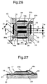
- Fig.26 is an enlarged view of the film acoustic wave device of Fig.25.
- Fig.27 is a cross-sectional view B-B of Fig.26.
- the wafer 11 made of silicon (Si) semiconductor; the film acoustic wave devices 12a ⁇ 12c; the orientation flat 13 showing standard surface of the wafer 11; the silicon (Si) semiconductor substrate 25; the ground electrode 15; the bonding pad 16 in equal electric potential with the ground electrode 15; the piezoelectric thin film 17 made of zinc oxide (ZnO); the upper electrodes 18a and 18b; the connecting patterns 19a and 19b; the bonding pads 20a and 20b respectively connected to the upper electrodes 18a and 18b; an etching hole 26; a dielectric thin film 27; and a hole 28.
- Si silicon
- the film acoustic wave devices 12a ⁇ 12c the orientation flat 13 showing standard surface of the wafer 11
- the silicon (Si) semiconductor substrate 25 the ground electrode 15; the bonding pad 16 in equal electric potential with the ground electrode 15
- the piezoelectric thin film 17 made of zinc oxide (ZnO)
- the upper electrodes 18a and 18b the connecting patterns 19a and 19b
- the shape of film acoustic wave device is changed, for example, the length Le of upper electrodes 18a and 18b, and the distance Lg between upper electrodes are changed similarly to the case of peripheral wafer 11 parallel to the direction of orientation flat 13 for the film acoustic wave device 12b, and the peripheral wafer 11 perpendicular to the direction of orientation flat 13 for the film acoustic wave device 12c.
- most suitable case to apply the method of changing the shape of film acoustic wave device concentrically is when the thickness of piezoelectric thin film 17 varies concentrically.
- the hole 28 located beneath the ground electrode 15 is made from frontal side of the upper electrodes 18a and 18b, by opening the etching hole 26 on the dielectric thin film 27 and removing part of the silicon (Si) semiconductor substrate 25 by an anisotropic etching from the etching hole 26.
- the acoustic resonance of film acoustic wave device 12 is satisfied with this air layer underneath the ground electrode 15.
- the method of opening the etching hole 26 via hole 21 can be made from the front as shown in Fig.27 or from the back as shown in Fig.24. In any which way, the properties of the film acoustic wave device 12 remain the same.
- Fig.27 between the semiconductor substrate 25 and ground electrode 15, there is the dielectric thin film 27, however, although it is omitted in the drawings of Figs.21 and 24, there are the dielectric thin films 27 for the actual film acoustic wave device 12.
- Fig.28 illustrates the film acoustic wave device for embodiment 11.
- Fig.29 is the enlarged diagram shown in Fig.28.
- Fig.30 is the cross-sectional view B-B of Fig.29.
- the wafer 11 made of gallium arsenide (GaAs) semiconductor substrate; the film acoustic wave devices 12a ⁇ 12c; the orientation flat 13 showing the standard surface of the wafer 11; the gallium arsenide (GaAs) semiconductor 14; the ground electrode 15; the bonding pads 16 in equal electric potential to the ground electrode 15; the piezoelectric thin film 17 made of aluminum nitride (AlN); the upper electrodes 18a and 18b; the connecting patterns 19a and 19b; the bonding pads 20a and 20b respectively connected to the upper electrodes 18a and 18b; the hole 28, a second electrode 29a that is not connected electrically to upper electrode 18a; and a second electrode 29b that is not electrically connected to 18b.
- GaAs gallium arsenide
- length Le2 of the second electrodes 29a and 29b, and distance Lg2 between the upper electrode 18a and the second electrode 29a are changed.
- the distance Lg2 is also a distance between the second electrode 29b and the upper electrode 18b.
- distance Lg2 between the second electrode 29a and upper electrode 18a are changed.
- the distances between the upper electrodes 18a and 18b with the second electrodes 29a and 29b, and length Le2 of the second electrodes 29a and 29b are changed.
- Such method for example, can be adopted not only when the thickness h of the piezoelectric thin film 17 is distributed, but also when the change in properties of the film acoustic wave device at the wafer 11 are differing at direction parallel and direction perpendicular to the orientation flat, due to the change in the component ratio of materials which the piezoelectric thin film 17 is being made of.
- the passband of film acoustic wave device 12b changes and in the direction perpendicular to the orientation flat 13, the passband and the band width of the film acoustic wave device 12c are changed, and in direction parallel to the orientation flat 13, passband of the film acoustic wave device 12b is compensated, and in the perpendicular direction both band width and passband of the film acoustic wave device 12c need be compensated, and need to change the way to change the forms of film acoustic wave device in directions parallel and perpendicular to the orientation flat 13.
- Fig.29 is the enlarged view of the film acoustic wave devices 12a, 12b and 12c of Fig.28.
- Fig.30 is cross-section B-B of Fig.29.
- the hole 28 is made without etching the gallium arsenide (GaAs) semiconductor substrate 14 on the lateral side of ground electrode 15.
- the properties of bulk acoustic wave filter is almost exactly same as the case of etching the gallium arsenide (GaAs) semiconductor substrate 14.
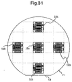
- Figs.31, 32 and 33 illustrate the acoustic wave for embodiment 12.
- the wafer 11 made of silicon (Si) semiconductor; the film acoustic wave devices 12a ⁇ 12c; the orientation flat 13 showing standard surface of the wafer 11; the silicon (Si) semiconductor substrate 25; the ground electrode 15; the bonding pads 16 at equal electric potential with the ground electrode 15; the piezoelectric thin film 17 made of lead titanate (PbTiO 3 ); the upper electrode of input side 18a; the upper electrode of output side 18b; the connecting patterns 19a and 19b; the bonding pads 20a and 20b connected respectively to the upper electrodes 18a and 18b; the second electrodes 29a and 29b that are not electrically connected to the upper electrodes 18a and 18b as in embodiment 11; a third electrode 30 that are not electrically connected to the upper electrodes 18a and 18b; an inductor 31; an electrode of capacitor 32; a connecting electrode 33 which electrically connects bonding pad 20a to the electrode of capacitor 32; and a dielectric substance layer 34 made of multi-layer of
- Figs.31 to 33 of the present embodiment an area of the capacitor electrode 32 is changed depending on the positioning at wafer 11. Resulting in approximately same effect as changing the capacitor C s1 of the equivalent circuit in Fig.4 the variation in property of the film acoustic wave device 12 on top of the wafer 11 is compensated.
- Fig.32 is the enlarged view of the film acoustic wave devices 12a, 12b and 12c of Fig.31.
- the third electrode 30 is placed in between the upper electrode of input side 18a and the upper electrode of output side 18b.
- Fig.33 is the cross-section B-B of Fig.32.
- a capacitor comprising the inductor 31 and the capacitor electrode 32 is electrically connected in parallel with the connecting electrode 33.
- the bonding pad of input side 20a is connected to the capacitor, however, the bonding pad of output side 20b can also be connected similarly. It is possible to change at least either one of the length Le3 of the third electrodes 30 and the distance Lg3 between the third electrodes 30 and the upper electrodes 18a and 18b.
- the resonant frequency can be compensated by changing the pattern shape of the film acoustic wave device 12, depending on the position at the wafer 11, to obtain the film acoustic wave devices with the same properties that does not depend on the positioning at wafer 11.
- piezoelectric ceramics with lead For use in the piezoelectric ceramics with lead, materials such as lead titanate (PbTiO 3 ) and PZT (PbTiO 3 -PbZrO 3 ) show excellent properties of the electromechanical coupling constant.
- these type of piezoelectric ceramics with lead are formed under a high temperature when making the thin film, therefore, the ceramics has a high melting point that it is essential to use chemically stable elements such as platinum (Pt) or gold (Au) for the ground electrode 15, and gallium arsenide (GaAs) semiconductor substrate and silicon (Si) semiconductor substrate as the substrate.
- Platinum (Pt) is excellent in the chemical stability.
- Lead titanate (PbTiO 3 ) is excellent material for Q, especially so as a material for a device that pre-conditions the use high frequency greater than GHz such as the film acoustic wave device.
- PbTiO 3 is excellent material for Q, especially so as a material for a device that pre-conditions the use high frequency greater than GHz such as the film acoustic wave device.
- ZnO zinc oxide
- AlN aluminum nitride
- the piezoelectric thin film 17 can have various properties by changing the ratio of constituents of lead titanate (PbTiO 3 ) and lead titanate-zirconate (PbZrO 3 ). A larger value of electromechanical coupling constant can be obtained using the PZT(PbTiO 3 -PbZrO 3 ) compared to just the lead titanate (PbTiO 3 ).
- Such type of piezoelectric thin film has a greater advantage upon designing.
- the PZT(PbTiO 3 -PbZrO 3 ) includes a numerous type of material compositions more than the lead titanate (PbTiO 3 ), it becomes difficult to form a film uniformly, and the compensation for variation property throughout wafer 11 is important.
- the electromechanical coupling constant of the piezoelectric ceramics that does not contain lead such as zinc oxide (ZnO) and aluminum nitride (AlN) are inferior to the piezoelectric ceramics with lead. However, they are characterized by a large value of Q.
- the large value of Q is ideal for a narrow band filter when configuring the filter.
- the narrow band filter results in the lag of passband from the necessary area. It is important to compensate the thickness distribution of the piezoelectric thin film 17 throughout the wafer 11, especially important to compensate the property variations inside the wafer 11. Also, this type of piezoelectric ceramics that does not contain lead, a forming temperature of the piezoelectric thin film is relatively low.
- this type of the piezoelectric ceramics it is possible for this type of the piezoelectric ceramics to use the glass substrate other than semiconductor substrates such as gallium arsenide (GaAs) or silicon (Si). It is also possible for this type of piezoelectric ceramics to use the ground electrode 15 other than platinum (Pt) or gold (Au), and even possible to use materials with low melting point such as aluminum (Al).
- the film acoustic wave device 12 has illustrated a multiple number of combinations of parameters namely: upper electrode 18, 18a and 18b; distance Lg between the upper electrode of input side 18a and upper electrode of output side 18b; length La and width Wa of connecting patterns 19, 19a and 19b; area of bonding pads 20, 20a, 20b; area of capacitor electrode 32 connected electrically to bonding pads 20a and 20b; length Le2 of second electrode 29a and 29b; distance Lg2 between second electrodes 29a and 29b to upper electrodes 18a and 18b; length Le3 of third electrode 30; distance Lg3 between the third electrode and upper electrodes 18a and 18b.
- changing one of the parameters is sufficient for the compensation.
- the parameters are: length Le and width We of upper electrodes 18, 18a and 18b; distance Lg between the upper electrode of input side 18a and the upper electrode of output side 18b; length La and width Wa of connecting patterns 19, 19a and 19b; area of bonding pads 20a and 20b; area of capacitor electrode 32 connected electrically to bonding pads 20a and 20b; length Le2 of second electrodes 29a and 29b; distance Lg2 between the second electrodes 29a and 29b with upper electrodes 18a and 18b; length Le3 of third electrode 30; distance Lg3 between the third electrodes 18a and 18b. That is, for optional combinations within these parameters, variation can be compensated at the top of wafer 11.
- pattern of the film acoustic wave devices shown in the Figs.7,9,11,13,15, 17,19,20,22,23,25,26,28,29,31 and 32 are some of the examples. There is no requirement to limit the pattern, and the pattern change to influence the property of film acoustic wave device is selective.
- film acoustic wave device there is no need to limit the cross-sectional shape of film acoustic wave device to those shown on Figs.21,24, 27,30 and 33.
- bulk acoustic wave resonator shown in Fig.23 is used as series and parallel elements of a ladder filter.
- the same effect can be obtained.
- the same effect will also be obtained by any combinations of cross-sectional shapes of film acoustic wave devices shown in Figs.21,24,27,30 and 33, and shapes of pattern of the film acoustic wave devices shown in Figs.7,9,11,13,15,17,19,20,22,23,25,26,28,29,31 and 32.
- the present invention by changing at least more than one of the pattern of film acoustic wave device, such as the length Le or width We of upper electrodes, the distance Lg between the upper electrodes of input/output side, the length La and width Wa of connecting pattern, the areas of bonding pads, the areas of electrode of capacitor connected electrically to bonding pads by the positioning at wafer, a variation of property for the film acoustic wave device that arises when positioning at wafer is reduced, and the film acoustic wave device with same properties that are not affected by the wafer positioning is obtained.
- the pattern of film acoustic wave device such as the length Le or width We of upper electrodes, the distance Lg between the upper electrodes of input/output side, the length La and width Wa of connecting pattern, the areas of bonding pads, the areas of electrode of capacitor connected electrically to bonding pads by the positioning at wafer
- piezoelectric thin film Without limiting the thickness of piezoelectric thin film, the type of materials for the film acoustic wave device or its combination, a variety of acoustic wave device that are useful in industries is achieved.
Landscapes
- Physics & Mathematics (AREA)
- Acoustics & Sound (AREA)
- Chemical & Material Sciences (AREA)
- Engineering & Computer Science (AREA)
- Ceramic Engineering (AREA)
- Crystallography & Structural Chemistry (AREA)
- Manufacturing & Machinery (AREA)
- Surface Acoustic Wave Elements And Circuit Networks Thereof (AREA)
- Piezo-Electric Or Mechanical Vibrators, Or Delay Or Filter Circuits (AREA)
Applications Claiming Priority (1)
| Application Number | Priority Date | Filing Date | Title |
|---|---|---|---|
| PCT/JP1997/001442 WO1998048464A1 (en) | 1997-04-24 | 1997-04-24 | Thin film piezoelectric element, method for manufacturing the same, and circuit element |
Publications (2)
| Publication Number | Publication Date |
|---|---|
| EP0952618A1 true EP0952618A1 (de) | 1999-10-27 |
| EP0952618A4 EP0952618A4 (de) | 2002-01-30 |
Family
ID=14180459
Family Applications (1)
| Application Number | Title | Priority Date | Filing Date |
|---|---|---|---|
| EP97919687A Withdrawn EP0952618A4 (de) | 1997-04-24 | 1997-04-24 | Piezoelektrische dünnschichtanordnung, verfahren zur herstellung derselben, und schaltungselement |
Country Status (5)
| Country | Link |
|---|---|
| US (2) | US6963155B1 (de) |
| EP (1) | EP0952618A4 (de) |
| JP (1) | JP3839492B2 (de) |
| KR (1) | KR20010073196A (de) |
| WO (1) | WO1998048464A1 (de) |
Cited By (2)
| Publication number | Priority date | Publication date | Assignee | Title |
|---|---|---|---|---|
| WO2006112260A1 (ja) | 2005-04-13 | 2006-10-26 | Murata Manufacturing Co., Ltd. | 圧電薄膜フィルタ |
| WO2012049373A1 (en) * | 2010-10-14 | 2012-04-19 | Teknologian Tutkimuskeskus Vtt | Changing operation frequency in a lbaw filter |
Families Citing this family (18)
| Publication number | Priority date | Publication date | Assignee | Title |
|---|---|---|---|---|
| FI107661B (fi) * | 1999-11-29 | 2001-09-14 | Nokia Mobile Phones Ltd | Menetelmä balansoidun suotimen keskitaajuuden säätämiseksi ja joukko balansoituja suotimia |
| GB0014963D0 (en) * | 2000-06-20 | 2000-08-09 | Koninkl Philips Electronics Nv | A bulk acoustic wave device |
| US6462460B1 (en) * | 2001-04-27 | 2002-10-08 | Nokia Corporation | Method and system for wafer-level tuning of bulk acoustic wave resonators and filters |
| JP2003023337A (ja) * | 2001-07-06 | 2003-01-24 | Murata Mfg Co Ltd | 圧電共振子およびフィルタ |
| US20050199972A1 (en) * | 2002-05-20 | 2005-09-15 | Lobl Hans P. | Bulk wave resonator and bulk wave filter |
| JP5358868B2 (ja) * | 2004-11-01 | 2013-12-04 | ブラザー工業株式会社 | 圧電アクチュエータ、圧電アクチュエータの製造方法、液体移送装置及び液体移送装置の製造方法 |
| US7466067B2 (en) * | 2004-11-01 | 2008-12-16 | Brother Kogyo Kabushiki Kaisha | Piezoelectric actuator, method for producing piezoelectric actuator, liquid transporting apparatus, and method for producing liquid transporting apparatus |
| US7294851B2 (en) * | 2004-11-03 | 2007-11-13 | Infineon Technologies Ag | Dense seed layer and method of formation |
| KR100639472B1 (ko) * | 2005-06-09 | 2006-10-27 | 주식회사 삼화양행 | 압전체의 주파수 특성 해석 방법 |
| KR100639473B1 (ko) * | 2005-06-16 | 2006-10-27 | 주식회사 삼화양행 | 압전체의 온도 변화에 따른 주파수 특성을 비선형적으로구하는 방법 |
| JP4791181B2 (ja) * | 2005-12-28 | 2011-10-12 | 京セラ株式会社 | 薄膜バルク音響波共振子、それを備えるフィルタおよび通信装置ならびに薄膜バルク音響波共振子の製造方法 |
| JP2007194390A (ja) * | 2006-01-19 | 2007-08-02 | Eudyna Devices Inc | 半導体発光装置の製造方法 |
| JP4877966B2 (ja) * | 2006-03-08 | 2012-02-15 | 日本碍子株式会社 | 圧電薄膜デバイス |
| US8704191B2 (en) * | 2010-01-20 | 2014-04-22 | Arizona Board Of Regents, A Body Corporate Of The State Of Arizona, Acting For And On Behalf Of Arizona State University | Film bulk acoustic wave resonator-based high energy radiation detectors and methods using the same |
| US8479363B2 (en) * | 2010-05-11 | 2013-07-09 | Hao Zhang | Methods for wafer level trimming of acoustically coupled resonator filter |
| US8776335B2 (en) * | 2010-11-17 | 2014-07-15 | General Electric Company | Methods of fabricating ultrasonic transducer assemblies |
| FR2973608A1 (fr) * | 2011-03-31 | 2012-10-05 | St Microelectronics Sa | Procede d'ajustement de la frequence de resonance d'un element vibrant micro-usine |
| DE102019111172B4 (de) * | 2019-04-30 | 2021-05-27 | RF360 Europe GmbH | BAW-Vorrichtung |
Family Cites Families (29)
| Publication number | Priority date | Publication date | Assignee | Title |
|---|---|---|---|---|
| US2799789A (en) * | 1949-04-06 | 1957-07-16 | John M Wolfskill | Piezoelectric crystal apparatus and method of making the same |
| US3401275A (en) * | 1966-04-14 | 1968-09-10 | Clevite Corp | Composite resonator |
| US3633134A (en) * | 1969-10-10 | 1972-01-04 | Motorola Inc | Crystal band pass filter circuit |
| JPS56149811A (en) | 1980-04-23 | 1981-11-19 | Hitachi Ltd | Elastic surface wave device and its preparation |
| US4320365A (en) | 1980-11-03 | 1982-03-16 | United Technologies Corporation | Fundamental, longitudinal, thickness mode bulk wave resonator |
| EP0092427B1 (de) * | 1982-04-20 | 1989-04-05 | Fujitsu Limited | Piezoelektrischer Resonator und Verfahren zur Abstimmung seiner Resonanzfrequenz |
| US4435441A (en) | 1982-12-30 | 1984-03-06 | The United States Of America As Represented By The Secretary Of The Army | Method of frequency trimming surface acoustic wave devices |
| JPS60189307A (ja) * | 1984-03-09 | 1985-09-26 | Toshiba Corp | 圧電薄膜共振器およびその製造方法 |
| JPS61269410A (ja) | 1985-05-23 | 1986-11-28 | Toshiba Corp | 薄膜弾性表面波装置 |
| JPS6278904A (ja) | 1985-10-02 | 1987-04-11 | Toshiba Corp | 圧電装置 |
| JPS62122405A (ja) | 1985-11-22 | 1987-06-03 | Sony Corp | 表面波素子の製造方法 |
| JPS6318708A (ja) | 1986-07-09 | 1988-01-26 | Fujitsu Ltd | 弾性表面波フイルタの周波数調整方法 |
| JPH01103012A (ja) | 1987-10-16 | 1989-04-20 | Hitachi Ltd | 表面弾性波素子およびその製造方法 |
| JPH01231411A (ja) | 1988-03-11 | 1989-09-14 | Toshiba Corp | 弾性表面波共振子フィルタの製造方法 |
| JPH02189011A (ja) | 1989-01-18 | 1990-07-25 | Fujitsu Ltd | 弾性表面波デバイスの製造方法 |
| JPH0388406A (ja) | 1989-04-11 | 1991-04-12 | Sanyo Electric Co Ltd | 弾性表面波素子 |
| JP3107381B2 (ja) | 1989-05-26 | 2000-11-06 | 株式会社日立製作所 | 弾性表面波デバイス |
| US5194836A (en) * | 1990-03-26 | 1993-03-16 | Westinghouse Electric Corp. | Thin film, microwave frequency manifolded filter bank |
| US5160870A (en) * | 1990-06-25 | 1992-11-03 | Carson Paul L | Ultrasonic image sensing array and method |
| US5075641A (en) * | 1990-12-04 | 1991-12-24 | Iowa State University Research Foundation, Inc. | High frequency oscillator comprising cointegrated thin film resonator and active device |
| US5185589A (en) * | 1991-05-17 | 1993-02-09 | Westinghouse Electric Corp. | Microwave film bulk acoustic resonator and manifolded filter bank |
| JPH05259804A (ja) * | 1992-03-13 | 1993-10-08 | Toyo Commun Equip Co Ltd | 超薄板多段縦続接続多重モ−ドフィルタ |
| JPH06204776A (ja) | 1992-12-28 | 1994-07-22 | Oki Electric Ind Co Ltd | 圧電薄膜振動子の製造方法 |
| JPH06252691A (ja) * | 1993-02-27 | 1994-09-09 | Nippon Dempa Kogyo Co Ltd | 水晶振動子 |
| JPH08274573A (ja) | 1995-03-29 | 1996-10-18 | Olympus Optical Co Ltd | マイクロ圧電振動子、その製法及び圧電トランスデューサ |
| US5759753A (en) | 1995-07-19 | 1998-06-02 | Matsushita Electric Industrial Co., Ltd. | Piezoelectric device and method of manufacturing the same |
| JP3924810B2 (ja) * | 1995-07-19 | 2007-06-06 | 松下電器産業株式会社 | 圧電素子とその製造方法 |
| US5692279A (en) * | 1995-08-17 | 1997-12-02 | Motorola | Method of making a monolithic thin film resonator lattice filter |
| US5971026A (en) | 1997-12-09 | 1999-10-26 | Honeywell Inc. | Internal geometry shape design for venturi tube-like gas-air mixing valve |
-
1997
- 1997-04-24 KR KR1020017003991A patent/KR20010073196A/ko not_active Ceased
- 1997-04-24 US US09/202,070 patent/US6963155B1/en not_active Expired - Fee Related
- 1997-04-24 JP JP54540398A patent/JP3839492B2/ja not_active Expired - Fee Related
- 1997-04-24 WO PCT/JP1997/001442 patent/WO1998048464A1/ja not_active Ceased
- 1997-04-24 EP EP97919687A patent/EP0952618A4/de not_active Withdrawn
-
2001
- 2001-02-08 US US09/778,872 patent/US7196452B2/en not_active Expired - Fee Related
Non-Patent Citations (2)
| Title |
|---|
| No further relevant documents disclosed * |
| See also references of WO9848464A1 * |
Cited By (4)
| Publication number | Priority date | Publication date | Assignee | Title |
|---|---|---|---|---|
| WO2006112260A1 (ja) | 2005-04-13 | 2006-10-26 | Murata Manufacturing Co., Ltd. | 圧電薄膜フィルタ |
| EP1871007A4 (de) * | 2005-04-13 | 2008-07-09 | Murata Manufacturing Co | Piezoelektrischer dünnschichtfilter |
| US7843285B2 (en) | 2005-04-13 | 2010-11-30 | Murata Manufacturing Co., Ltd. | Piezoelectric thin-film filter |
| WO2012049373A1 (en) * | 2010-10-14 | 2012-04-19 | Teknologian Tutkimuskeskus Vtt | Changing operation frequency in a lbaw filter |
Also Published As
| Publication number | Publication date |
|---|---|
| EP0952618A4 (de) | 2002-01-30 |
| US7196452B2 (en) | 2007-03-27 |
| WO1998048464A1 (en) | 1998-10-29 |
| KR20010073196A (ko) | 2001-07-31 |
| US20010038255A1 (en) | 2001-11-08 |
| US6963155B1 (en) | 2005-11-08 |
| JP3839492B2 (ja) | 2006-11-01 |
Similar Documents
| Publication | Publication Date | Title |
|---|---|---|
| EP0952618A1 (de) | Piezoelektrische dünnschichtanordnung, verfahren zur herstellung derselben, und schaltungselement | |
| US6507983B1 (en) | Method of making tunable thin film acoustic resonators | |
| US7005946B2 (en) | MEMS piezoelectric longitudinal mode resonator | |
| US7170215B2 (en) | Electronic component and method for manufacturing the same | |
| CN100492896C (zh) | 滤波器的改良 | |
| EP0973256B1 (de) | Piezoelektrische dünnschichtanordnung | |
| KR100804407B1 (ko) | 탄성 경계파 장치의 제조방법 | |
| EP0602666B1 (de) | Akustische Oberflächenwellenanordnung mit Interdigitalwandler auf einem Substrat-Träger und Verfahren zur Herstellung | |
| JP3996379B2 (ja) | 圧電共振子を含むフィルタ構造および構成 | |
| US6864619B2 (en) | Piezoelectric resonator device having detuning layer sequence | |
| KR100756096B1 (ko) | 듀플렉서 | |
| EP0083237B1 (de) | Keramischer Resonator und keramischer Filter mit einem solchen keramischen Resonator | |
| DE10142157A1 (de) | Schallwellenresonator und Verfahren zum Betreiben desselben, um die Resonanz beizubehalten, wenn dieser Temperaturänderungen ausgesetzt wird | |
| JPWO1998048464A1 (ja) | 薄膜圧電素子及び薄膜圧電素子の製造方法及び回路素子 | |
| US4166257A (en) | Capacitively weighted surface acoustic wave device | |
| US7320164B2 (en) | Method of manufacturing an electronic component | |
| CA2259034A1 (en) | Thin film piezoelectric element, method for manufacturing the same, and circuit element | |
| KR100359967B1 (ko) | 박막압전소자및박막압전소자의제조방법및회로소자 | |
| CN118282348A (zh) | 具有用于改进耦合的对称涂层材料的声学谐振器 | |
| CN119382653A (zh) | 电极与压电层之间的用于控制耦合的金属层 |
Legal Events
| Date | Code | Title | Description |
|---|---|---|---|
| PUAI | Public reference made under article 153(3) epc to a published international application that has entered the european phase |
Free format text: ORIGINAL CODE: 0009012 |
|
| 17P | Request for examination filed |
Effective date: 19981210 |
|
| AK | Designated contracting states |
Kind code of ref document: A1 Designated state(s): DE FR GB |
|
| A4 | Supplementary search report drawn up and despatched |
Effective date: 20011213 |
|
| AK | Designated contracting states |
Kind code of ref document: A4 Designated state(s): DE FR GB |
|
| RIC1 | Information provided on ipc code assigned before grant |
Free format text: 7H 01L 41/107 A, 7H 03H 3/013 B, 7H 03H 9/17 B |
|
| RAP1 | Party data changed (applicant data changed or rights of an application transferred) |
Owner name: MITSUBISHI DENKI KABUSHIKI KAISHA |
|
| STAA | Information on the status of an ep patent application or granted ep patent |
Free format text: STATUS: THE APPLICATION HAS BEEN WITHDRAWN |
|
| 18W | Application withdrawn |
Effective date: 20070710 |