EP0953961A2 - Verfahren und Einrichtung zum Steuern eines Flüssigkristallanzeigegeräts - Google Patents
Verfahren und Einrichtung zum Steuern eines Flüssigkristallanzeigegeräts Download PDFInfo
- Publication number
- EP0953961A2 EP0953961A2 EP99303371A EP99303371A EP0953961A2 EP 0953961 A2 EP0953961 A2 EP 0953961A2 EP 99303371 A EP99303371 A EP 99303371A EP 99303371 A EP99303371 A EP 99303371A EP 0953961 A2 EP0953961 A2 EP 0953961A2
- Authority
- EP
- European Patent Office
- Prior art keywords
- liquid crystal
- voltage
- pixel
- transmittance
- driving method
- Prior art date
- Legal status (The legal status is an assumption and is not a legal conclusion. Google has not performed a legal analysis and makes no representation as to the accuracy of the status listed.)
- Withdrawn
Links
Images


Classifications
-
- G—PHYSICS
- G09—EDUCATION; CRYPTOGRAPHY; DISPLAY; ADVERTISING; SEALS
- G09G—ARRANGEMENTS OR CIRCUITS FOR CONTROL OF INDICATING DEVICES USING STATIC MEANS TO PRESENT VARIABLE INFORMATION
- G09G3/00—Control arrangements or circuits, of interest only in connection with visual indicators other than cathode-ray tubes
- G09G3/20—Control arrangements or circuits, of interest only in connection with visual indicators other than cathode-ray tubes for presentation of an assembly of a number of characters, e.g. a page, by composing the assembly by combination of individual elements arranged in a matrix no fixed position being assigned to or needed to be assigned to the individual characters or partial characters
- G09G3/34—Control arrangements or circuits, of interest only in connection with visual indicators other than cathode-ray tubes for presentation of an assembly of a number of characters, e.g. a page, by composing the assembly by combination of individual elements arranged in a matrix no fixed position being assigned to or needed to be assigned to the individual characters or partial characters by control of light from an independent source
- G09G3/36—Control arrangements or circuits, of interest only in connection with visual indicators other than cathode-ray tubes for presentation of an assembly of a number of characters, e.g. a page, by composing the assembly by combination of individual elements arranged in a matrix no fixed position being assigned to or needed to be assigned to the individual characters or partial characters by control of light from an independent source using liquid crystals
- G09G3/3611—Control of matrices with row and column drivers
- G09G3/3648—Control of matrices with row and column drivers using an active matrix
- G09G3/3651—Control of matrices with row and column drivers using an active matrix using multistable liquid crystals, e.g. ferroelectric liquid crystals
-
- G—PHYSICS
- G09—EDUCATION; CRYPTOGRAPHY; DISPLAY; ADVERTISING; SEALS
- G09G—ARRANGEMENTS OR CIRCUITS FOR CONTROL OF INDICATING DEVICES USING STATIC MEANS TO PRESENT VARIABLE INFORMATION
- G09G2310/00—Command of the display device
- G09G2310/06—Details of flat display driving waveforms
-
- G—PHYSICS
- G09—EDUCATION; CRYPTOGRAPHY; DISPLAY; ADVERTISING; SEALS
- G09G—ARRANGEMENTS OR CIRCUITS FOR CONTROL OF INDICATING DEVICES USING STATIC MEANS TO PRESENT VARIABLE INFORMATION
- G09G2310/00—Command of the display device
- G09G2310/06—Details of flat display driving waveforms
- G09G2310/061—Details of flat display driving waveforms for resetting or blanking
-
- G—PHYSICS
- G09—EDUCATION; CRYPTOGRAPHY; DISPLAY; ADVERTISING; SEALS
- G09G—ARRANGEMENTS OR CIRCUITS FOR CONTROL OF INDICATING DEVICES USING STATIC MEANS TO PRESENT VARIABLE INFORMATION
- G09G3/00—Control arrangements or circuits, of interest only in connection with visual indicators other than cathode-ray tubes
- G09G3/20—Control arrangements or circuits, of interest only in connection with visual indicators other than cathode-ray tubes for presentation of an assembly of a number of characters, e.g. a page, by composing the assembly by combination of individual elements arranged in a matrix no fixed position being assigned to or needed to be assigned to the individual characters or partial characters
- G09G3/2007—Display of intermediate tones
- G09G3/2011—Display of intermediate tones by amplitude modulation
-
- G—PHYSICS
- G09—EDUCATION; CRYPTOGRAPHY; DISPLAY; ADVERTISING; SEALS
- G09G—ARRANGEMENTS OR CIRCUITS FOR CONTROL OF INDICATING DEVICES USING STATIC MEANS TO PRESENT VARIABLE INFORMATION
- G09G3/00—Control arrangements or circuits, of interest only in connection with visual indicators other than cathode-ray tubes
- G09G3/20—Control arrangements or circuits, of interest only in connection with visual indicators other than cathode-ray tubes for presentation of an assembly of a number of characters, e.g. a page, by composing the assembly by combination of individual elements arranged in a matrix no fixed position being assigned to or needed to be assigned to the individual characters or partial characters
- G09G3/34—Control arrangements or circuits, of interest only in connection with visual indicators other than cathode-ray tubes for presentation of an assembly of a number of characters, e.g. a page, by composing the assembly by combination of individual elements arranged in a matrix no fixed position being assigned to or needed to be assigned to the individual characters or partial characters by control of light from an independent source
- G09G3/36—Control arrangements or circuits, of interest only in connection with visual indicators other than cathode-ray tubes for presentation of an assembly of a number of characters, e.g. a page, by composing the assembly by combination of individual elements arranged in a matrix no fixed position being assigned to or needed to be assigned to the individual characters or partial characters by control of light from an independent source using liquid crystals
- G09G3/3611—Control of matrices with row and column drivers
- G09G3/3614—Control of polarity reversal in general
Definitions
- the present invention relates to a driving method for a liquid crystal device allowing a high-speed drive for gradational display according to the active matrix scheme.
- liquid crystal display apparatus Various types of liquid crystal materials are used in liquid crystal display apparatus, inclusive of nematic liquid crystals, smectic liquid crystals and polymer dispersion-type liquid crystals.
- a liquid crystal device exhibiting a spontaneous polarization and bistability has been proposed by Clark and Lagerwall in U.S. Patent No. 4,367,924, etc.
- the bistable liquid crystal a ferroelectric liquid crystal in chiral smectic C phase (SmC*) or H phase (SmH*) is generally used.
- the liquid crystal exhibits bistable states, i.e., a first optically stable state and a second optically stable state, in response to an electric field applied thereto, and also a memory characteristic, i.e., a property that the resultant first or second optically stable state is retained as it is in the absence of an electric field.
- the liquid crystal device also quickly responds to a change in electric field and accordingly is expected to be widely utilized in the field of high-speed memory-type display apparatus.
- the former anti-ferroelectric liquid crystal device effects a picture display by utilizing the stability of an alignment state possessed by the anti-ferroelectric liquid crystal. More specifically, the anti-ferroelectric liquid crystal assumes three stable states in alignment of liquid crystal molecules. In response to a voltage exceeding a first threshold, the liquid crystal is oriented to a first ferroelectric phase wherein liquid crystal molecules are aligned in a first direction or a second ferroelectric phase wherein liquid crystal molecules are aligned in a second direction depending on the polarity of the applied voltage, and in response a voltage below a second threshold which is lower than the first threshold, the liquid crystal is oriented to an anti-ferroelectric phase which is an intermediate alignment state between the first and second ferroelectric phases. If the transmission axes of a pair of polarizers disposed on both sides of the liquid crystal device are set with reference to the optical axis in the anti-ferroelectric phase, the optical transmittance through the device can be controlled to effect a picture display.
- JP-A 7-64056 discloses a scheme wherein a writing voltage is applied to a liquid crystal placed in a ferroelectric phase or an anti-ferroelectric phase.
- the above-mentioned ferroelectric liquid crystal and antiferroelectric liquid crystal both have a spontaneous polarization and therefore cause a current (i.e., an inversion current) accompanying the inversion of the spontaneous polarization at the time of the switching of liquid crystal molecules.
- the inversion current flows in a direction of obstructing the external electric field, i.e., in a direction of consuming an electric charge stored in a liquid crystal capacitance via a switching device.
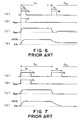
- FIG. 6 is an example of time chart for driving a thresholdless antiferroelectric liquid crystal device as described above according to a known active matrix scheme.
- a scanning signal voltage waveform applied to switching devices on an arbitrarily selected scanning signal line wherein T G represents a scanning selection period.
- a data signal voltage waveform applied to a pixel electrode via a switching device at a certain pixel on the selected scanning signal line.
- a voltage waveform applied to the liquid crystal layer at the pixel.
- a transmittance change at the pixel wherein the darkest state is represented as 0 % and the brightest state is represented as 100 %.
- FIG. 6 At (d) of Figure 6 is illustrated a pixel intended to display a 100 % display state in a frame period T F1 and a 0 % display state in a frame period T F2 .
- a selection period T G in the frame period T F2 at (d) if the switching to a 0 % state is not completed within the selection period T G , the voltage applied across the liquid crystal layer at the pixel is raised by an inversion current due to liquid crystal molecules switched in a subsequent non-selection period as shown at (c), whereby the intended 0 % display is failed as shown at (d).
- the selection period Tg is extended so as to ensure the liquid crystal switching to the 0 % state as shown in Figure 7, the frame frequency is lowered (i.e., the frame period T F1 , T F2 ... is increased).
- a principal object of the present invention is to provide a driving method for a liquid crystal device using a liquid crystal having a spontaneous polarization capable of a high-speed drive for desired gradational display.
- a driving method for a liquid crystal device of the active matrix-type comprising a pair of substrates, a layer of liquid crystal having a spontaneous polarization disposed between the substrates so as to form two-dimensionally arranged pixels disposed along a plurality of rows and a plurality of columns, and a switching device disposed at each pixel so as to control a voltage applied to the liquid crystal at the pixel;
- the driving method comprising a frame operation including: dividing a scanning selection period for each selected row into a first period and a second period in a current frame, in the first period, applying a reset pulse to the liquid crystal at each pixel on the selected row, the reset pulse having a polarity opposite to that of a writing pulse voltage applied to the liquid crystal at the pixel in a previous frame, thereby resetting the pixels on the selected row to a first transmittance, and in the second period, applying a writing pulse of a prescribed voltage to the liquid crystal at each pixel to establish a prescribed transmittance for
- the voltage value of the reset pulse may be selected for each pixel based on a display state at the pixel in a previous frame, whereby the performance of resetting to the first transmittance can be improved to allow rewriting into desired gradation levels in a shorter period.
- a non-selection period is interposed between the first period for applying the reset pulse and the second period for applying the writing pulse, whereby the period in which a pixel is completely transformed into a state of the first transmittance can be used for scanning selection of (an)other line(s), to realize a further shorter one-frame scanning period.
- the drive is performed by a frame-inversion mode in which the voltage value of the reset pulse is determined based on a display state in the previous frame and a prescribed display state in the current frame, respectively at a pixel concerned, whereby one-frame scanning period can be further shortened.
- the driving method according to the present invention is preferably applied to a thresholdless anti-ferroelectric liquid crystal device as described above, but is also preferably applicable to another type of liquid crystal device having a similar voltage-transmittance characteristic to realize a good gradational display at a high speed.
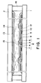
- Figure 1 is a schematic sectional view of an example of liquid crystal device to which the driving method according to the invention is applied.
- Figure 2 is a schematic plan view of a liquid crystal display apparatus including the liquid crystal device of Figure 1.
- Figure 3 illustrates a relationship between an average molecular axis direction of liquid crystal molecules and polarization axes of polarizers in a liquid crystal device using TLAFLC (threshold anti-ferroelectric liquid crystal) used in the invention.
- TLAFLC threshold anti-ferroelectric liquid crystal
- Figure 4 is a graph showing a voltage-transmittance curve of a liquid crystal device used in the invention.
- Figure 5 is a time chart according to a first embodiment of the invention.
- Figures 6 and 7 are respectively a time chart for a conventional driving method for a liquid crystal device using TLAFLC.
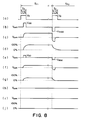
- Figure 8 is a time chart for illustrating a manner of setting a reset pulse in the first embodiment of the invention.
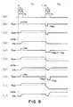
- Figure 9 is a time chart for illustrating a manner of rewriting a 50 %-display pixel into 0 - 100 % display states in the first embodiment of the invention.
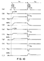
- Figure 10 is a time chart for illustrating a case of applying reset pulses of an identical voltage value to pixels having displayed different gradation levels.
- Figure 11 is a time chart according to a second embodiment of the invention.
- Figure 12 is a time chart according to a third embodiment of the invention.
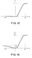
- Figures 13 and 14 are respectively a graph showing another voltage-transmittance characteristic of a liquid crystal device used in the invention.
- Figure 1 is a schematic sectional view of an active matrix-type liquid crystal device to be driven by a driving method according to the present invention
- Figure 2 is a schematic plan view of a liquid crystal display apparatus incorporating the liquid crystal deice of Figure 1.
- the liquid crystal device includes a pair of substrates 1 and 2 and a liquid crystal 15 disposed between the substrates in a space surrounded by a sealing member 16.
- the substrates 1 and 2 are ordinarily formed of an insulating transparent sheet, such as a glass sheet.
- pixel electrodes 9 and TFTs 8 as switching devices are disposed in a two-dimensional matrix.
- Each pixel electrode 9 is formed of a transparent electroconductive material, such as ITO (indium tin oxide) and has an area of, e.g., 200 - 100 ⁇ m x 200 - 100 ⁇ m.
- Each TFT 8 comprises a gate electrode 3 formed on the substrate 1, a gate insulating film 5 coating the gate electrode 3 and comprising silicon nitride (SiN), etc., a semiconductor layer 4 formed on the gate insulating film 5 so as to be opposite to the gate electrode 3, a source electrode 7 connected, to one side of the semiconductor layer 4, and a drain electrode 6 connected to the other side of the semiconductor layer 4.
- TFT 8 is turned on to have an ON-resistance R ON of ca. 100 k ⁇ , for example, when the gate electrode 3 is supplied with a gate pulse (scanning selection signal).
- the gate electrode 3 of TFT 8 at each pixel is connected to a scanning signal line 23 of a corresponding row, the drain electrode 6 is connected to a corresponding pixel electrode 9, and the source electrode 7 is connected to a data signal line of a corresponding column.
- each scanning signal line 32 is connected to a scanning signal application circuit 21, and each data signal line 24 and holding capacitor (supplementary capacitor) electrode 10 of ITO film are connected to a data signal application circuit 22.
- the scanning signal application circuit 21 sequentially supplies a scanning selection signal to the respective scanning signal lines 23 for turning on the gates of TFTs 8 on each line.
- the data signal application circuit 22 applies gradation pulses having absolute values corresponding to gradation levels to be displayed at the pixels to the corresponding data signal line 24.
- the pixel electrodes 9 and TFTs 8 are coated with an alignment film 12.
- a common electrode 13 is disposed opposite to the pixel electrodes 9 so as to be supplied with a reference voltage Vcom, and an alignment film 14 is formed thereon.
- the common electrode 13 is formed of a transparent conductive material such as ITO.
- the alignment films 12 and 14 may be formed of, e.g., a polyimide-based homogeneous alignment material, and the surface thereof may be subjected to an aligning treatment, such as rubbing in prescribed directions.
- silica beads of 2.0 ⁇ m in average diameter were dispersed on one substrate so as to provide a uniform cell gap between the substrates 1 and 2, and 200 scanning signals 23 and 960 data signal lines 24 were formed on the substrate 1 so as to provide a color liquid crystal device having a diagonal picture area size of 6 inches and 320x200 pixels each comprising sub-color pixels of R, G and B.
- the liquid crystal device constituted may be sandwiched between a pair of polarizers so as to provide a transmission-type display device.
- the above-described liquid crystal device structure is just an example, and the driving method of the present invention is applicable to any active matrix-type liquid crystal device capable of controlling a voltage applied to the liquid crystal at each pixel by means of a switching device and having a desired voltage-transmittance characteristic.
- the liquid crystal suitably used in the present invention is one having a spontaneous polarization.
- the liquid crystal material and device arrangement may suitably be designed to provide the liquid crystal 15 with a desired voltage-transmittance characteristic such that the liquid crystal 15 assumes a first alignment state exhibiting a first transmittance under no electric field, is realigned or tilted from the first alignment state to a second alignment state in one direction when supplied with a voltage of a first polarity to exhibit a second transmittance at a prescribed voltage V 0 , and is realigned or tilted from the first alignment state to a third alignment state in another directions when supplied with a voltage of a second polarity opposite to the second polarity to exhibit a second transmittance at a prescribed voltage -V 0 , and the liquid crystal 15 changes its transmittance continuously between the first transmittance and the second transmittance depending on a voltage applied thereto.
- TLAFLC thresholdless antiferroelectric liquid crystal
- Figure 3 illustrates a relationship between several average molecular axis directions of TLAFLC molecules and polarization axes of polarizers
- Figure 4 illustrates a voltage-transmittance characteristic, respectively, of a TLAFLC device used in the present invention.
- TLAFLC is sealed between the substrates with a gap smaller than the helical pitch thereof, so that its helical structure is lost.
- Vsat saturation voltage
- the molecular (longer) axes of substantially all the liquid crystal molecules are oriented to a third direction 32b, thus also providing a ferroelectric phase.
- the application voltage is zero, the liquid crystal molecules are disposed in smectic layers and alternately oriented in the second direction 32a or the third direction 32b layer by layer, so that the spontaneous polarizations of the respective layers are canceled with each other to provide an anti-ferroelectric phase.
- the average direction (director) of the liquid crystal molecular (longer) axes are aligned substantially in a direction of the smectic layer normal of the liquid crystal, i.e., a first direction 32c which is substantially intermediate the second direction 32a and the third direction 32b.
- a pair of polarizers are disposed so that a transmission axis 31a of one polarizer is disposed in substantially parallel to the smectic layer normal direction, and a transmission axis 31b of the other polarizer is disposed perpendicular to the transmission axis 31a.
- the liquid crystal device exhibits the highest transmittance (the brightest display state) in the second or third alignment state wherein the liquid crystal director is oriented in the second or third direction 32a or 32b, and the lowest transmittance (the darkest display state) in the first alignment state wherein the liquid crystal director is oriented in average in the intermediate direction 32c which is substantially parallel to the smectic layer normal.
- the director of the liquid crystal is continuously changed between the second direction 32a and the third direction 32b depending on the polarity and voltage value (absolute value) of the applied voltage. Accordingly, in the liquid crystal device, the transmittance of each pixel can be continuously changed by controlling the voltage applied to the liquid crystal thereat. Incidentally, if the set positions of the polarization axes of the polarizers are changed, it is possible to set a maximum transmittance at an applied voltage of zero and a minimum transmittance at a voltage exceeding the saturation voltage.
- Figure 5 is a time chart for practicing a first embodiment of the driving method according to the present invention. Incidentally, with respect to data signal voltage waveforms shown in Figures 5 - 12, only a data signal synchronized with a noted scanning signal line is shown and other data signals are omitted from showing for the convenience of illustration.
- FIG. 5 at (a) is shown a scanning selection signal voltage waveform applied to pixels on an arbitrary line, at (b) is shown a data signal voltage waveform applied to one of the pixels on the line, at (c) is shown a voltage waveform applied to the liquid crystal at the pixel, and at (d) is shown a corresponding transmittance change at the pixel wherein the brightest transmittance level is denoted as 100 % and the darkest transmittance level is denoted as 0 %.
- This embodiment adopts a frame inversion drive scheme wherein the polarity of a writing voltage applied to a pixel for display is inverted for each frame.
- a scanning selection period is divided into sub-periods t 1 and t 2 (which are equal to each other in this embodiment), and in the period t 1 , a reset pulse of a polarity opposite to that of a writing pulse voltage applied in a previous frame is applied to the liquid crystal to provide a 0 %-display state during the period t 1 . More specifically, in case where a writing voltage pulse of a positive polarity is applied in a previous frame T F1 for providing a 100 %-display state, a reset pulse of a negative polarity is applied.
- Liquid crystal molecules supplied with the reset pulse of an opposite polarity are switched toward the opposite direction (i.e., from 32a toward 32b, or from 32b toward 32a in Figure 3), so that the rewriting can be performed at a faster speed than when the voltage applied to the liquid crystal is simply made zero, thus within a period t 1 which is much shorter than the period T G shown in Figure 7.
- a writing pulse corresponding to a desired display state in a frame T F2 is applied so as to effect a rewriting from the dark state to a bright state, which is fast by nature. Accordingly, a sufficient rewriting is effected within a selection period T G which is much shorter than that required in the conventional scheme, so that a time for effectively displaying a desired gradation level within one frame is extended to effect an accurate gradational display.
- the liquid crystal device As described with reference to Figure 4, the liquid crystal device according to this embodiment exhibits a minimum transmittance when a voltage of zero is applied to the liquid crystal and also transmittances which increase depending on absolute values of voltages applied to the liquid crystal. Accordingly, if an excessively large value of reset voltage is applied, the liquid crystal can pass through a 0 %-display state to reach a bright display state within the period t 1 . This phenomenon is illustrated in Figure 10.
- At (a) is shown a scanning selection signal voltage waveforms applied to data signal lines each connected to one of the pixels on the line; at (b), (e) and (h) are shown data signal voltage waveforms applied to data signal lines each connected to one of the pixels on the line; at (c), (f) and (i) are shown voltage waveforms applied to the liquid crystal at the corresponding pixels; and at (d), (g) and (j) are shown resultant transmittance changes at the respective pixels.
- the waveforms at (b) - (d) represent a case of 100 %-display
- the waveforms at (e) - (g) represent a case of 50 %-display
- the waveforms at (h) - (j) represent a case of 0 %-display, respectively in a first frame T F1 .
- a 0 %-display is intended in a second frame T F2 .
- the pixel of 100 % display assumes a substantially 0 %-display state after the period t 1 as shown at (d), but the pixels of 50 %-display and 0 %-display cause overswitching by the reset pulses and pass through the intended 0 %-display state to reach bright display states showing a transmittance exceeding 0 %.
- some pixels can fail to display an intended 0 %-display state.
- the voltage value of a reset pulse is selected depending on a display state in a previous frame T F1 . More specifically, as shown in Figure 8, a pixel having exhibited a 100 %-display state in a previous frame T F1 is supplied with a reset pulse having a voltage value -V R100 which has an opposite polarity and an identical absolute value to a writing pulse voltage value of V 100 for the 100 %-display in the period t 1 of a subsequent frame T F2 as shown at (b).
- pixels having a 0 %-display state and an intermediate 50 %-display state are supplied with a reset pulse of voltage zero and a reset pulse of -V R50 which has an opposite polarity and an identical absolute value to the intermediate voltage V 50 for the intermediate 50 %-display state, respectively in the period t 2 of T F2 , thereby providing substantially 0 %-display state without overswitching to a bright display state.
- Figure 9 is a time chart for illustrating a case of rewriting pixels each having exhibited a 50 %-display state into 0 %-, 50 %- and 100 %-display states, respectively.
- a scanning selection signal voltage waveform applied to pixels on an arbitrary line
- at (b), (e) and (h) are shown data signal voltage waveforms applied to data signal lines each connected to one of the pixels on the line
- at (c), (f) and (i) are shown voltage waveforms applied to the liquid crystal at the corresponding pixels
- at (d), (g) and (j) are shown resultant transmittance changes at the respective pixels.
- the waveforms at (b) - (d) represent a case of 0 %-display
- the waveforms at (e) - (g) represent a case of 50 %-display
- the waveforms at (h) - (j) represent a case of 100 %-display, respectively in a second frame T F2 .
- This embodiments has been explained with reference to a frame-inversion drive scheme wherein the polarity of a writing voltage applied to a pixel for display is inverted for each frame, but this embodiment is also applicable to a scheme free from polarity inversion of writing pulses or a scheme wherein polarity inversion of writing pulses is effected in every plurality of frames.
- FIG. 11 is a time chart therefor.
- a scanning selection signal voltage waveform applied to pixels on an arbitrary line
- at (b), (e) and (h) are shown data signal voltage waveforms applied to data signal lines each connected to one of the pixels on the line
- at (c), (f) and (i) are shown voltage waveforms applied to the liquid crystal at the corresponding pixels
- at (d), (g) and (j) are shown resultant transmittance changes at the respective pixels.
- the waveforms at (b) - (d) represent a case of 100 %-display
- the waveforms at (e) - (g) represent a case of 50 %-display
- the waveforms at (h) - (j) represent a case of 0 %-display, respectively in a first frame T F1 .
- a 0 %-display state is intended to be formed.
- a non-selection period t 3 is interposed between divided scanning selection periods t 1 and t 2 .
- a reset pulse determined depending on a display state in a previous frame of a pixel is applied to the pixel to reset the pixel into a 0 %-display state.
- a TFT for a selected line is once turned off after the period t 1 to maintain the application of a reset pulse voltage to the pixels on the selected for a period t 3 necessary for completing the resetting of the periods into the 0 %-display state.
- the TFT is again turned on for a period t 2 to apply writing pulse voltages to the pixels on the selected line.
- the non-selection period t 3 between the scanning selection period t 1 and t 2 can be used for scanning selection of another line or other lines so that a selection period for one line can be substantially reduced to provide an increased frame frequency.
- this embodiments has been explained with reference to a frame-inversion drive scheme wherein the polarity of a writing voltage applied to a pixel for display is inverted for each frame, but this embodiment is also applicable to a scheme free from polarity inversion of writing pulses or a scheme wherein polarity inversion of writing pulses is effected in every plurality of frames.
- FIG. 12 is a time chart for this embodiment.
- a scanning selection signal voltage waveform applied to pixels on an arbitrary line
- at (b), (e) and (h) are shown data signal voltage waveforms applied to data signal lines each connected to one of the pixels on the line
- at (c), (f) and (i) are shown voltage waveforms applied to the liquid crystal at the corresponding pixels
- at (d), (g) and (j) are shown resultant transmittance changes at the respective pixels.
- the waveforms at (b) - (d) represent a case of 0 %-display
- the waveforms at (e) - (g) represent a case of 50 %-display
- the waveforms at (h) - (j) represent a case of 100 %-display, respectively in a second frame T F2 .
- the pixels having exhibited a 50 %-display state in T F1 are supplied with reset pulses which are determined based on a display state formed in a previous frame and a display state to be formed in a current frame of the respective pixels.
- reset pulses which are determined based on a display state formed in a previous frame and a display state to be formed in a current frame of the respective pixels.
- this characteristic is rather utilized to determine a reset pulse by adding a voltage value for providing a display state in a current frame to a voltage value set with reference a display state attained in the previous frame, thereby rewriting the pixel concerned into a display state closer to the one intended to be formed in the current frame.
- a reset pulse having a voltage value (-V R50 ) determined corresponding to a previous display state of 50 % is applied in the period t 1 similarly as in the first embodiment.
- the reset pulse therefor is determined by adding a writing pulse voltage value (-V 50 ) for a 50 %-display state to a reset voltage value (-V R50 ) so as to reset the pixel to a 0 %-display state in an early period within the period t 1 and further start the rewriting to a bright state within the period t 1 .
- a writing pulse having a voltage value (-V 50 ) for a prescribed 50 %-display state is applied to hold the pixel already having an increased transmittance at the 50 %-display level.
- the reset pulse voltage value is determined by adding a writing pulse voltage value (-V 100 ) for a 100 %-display to a reset voltage value (-V R50 ) so as to reset the pixel to a 0 %-display state in an earlier period within the period t 1 earlier than in the case of 50 %-display and further start the rewriting to a bright state within the period t 1 .
- the reset pulse voltage (-V R50-100 ) exceeds a saturation voltage necessary for a 100 %-display, so that a writing pulse voltage (-V 100 ) required for a prescribed 100 %-display is applied to the pixel to hold the pixel at the 100 %-display level.
- the rewriting into a display state of a current frame is started at a point of time at which the 0 %-display state is realized within the period t 1 , so that the rewriting period t 2 can be shortened than in the first embodiment and therefore the one-line scanning selection period can be effectively shortened to provide an increased frame frequency.
- a liquid crystal device having a voltage (V) - transmittance (T) characteristic as shown in Figure 13 can also be driven according to the first third embodiments of the driving method according to the present invention explained with reference to Figures 8 and 9, Figure 11, and Figure 12, respectively, to attain similar effects as obtained by using a liquid crystal device having a voltage (V) - transmittance (T) characteristic as shown in Figure 4.
- a liquid crystal device having a V-T characteristic shown in Figure 13 can be formed by using a liquid crystal material exhibiting a chiral smectic phase, of which the composition is adjusted to preferably contain at most 50 wt. % of compounds having an ester skeleton, and further by appropriate adjustment of the liquid crystal material treatment, the device structure including a material, and a treatment condition for alignment control films.
- the V-T characteristic of Figure 13 is realized by a liquid crystal device wherein the liquid crystal molecules are aligned to provide an average molecular axis substantially coinciding with an average uniaxial aligning treatment axis to be monostabilized in the absence of an electric field applied thereto and, under application of voltages of one polarity (a first polarity), are realigned to provide a tilt angle which varies continuously from the average molecular axis of the monostabilized position depending on the magnitude of the applied voltage, but under application of voltages of the other polarity (i.e., a second polarity opposite to the first polarity), the liquid crystal molecules are not substantially tilted but provide an average molecular axis substantially coinciding with the average molecular axis under no electric field regardless of the magnitude of the applied voltages.
- a first polarity a first polarity
- the liquid crystal material showing a chiral smectic phase may preferably exhibit a phase transition series on temperature decrease of I (isotropic) phase - Ch (cholesteric) phase - SmC* (chiral smectic) phase or I phase - SmC* phase and be placed in a non-memory state in the SmC* phase.
- a liquid crystal device having a voltage (V) - transmittance (T) characteristic as shown in Figure 14 can also be driven according to the first to third embodiments of the driving method according to the present invention explained with reference to Figures 8 and 9, Figure 11, and Figure 12, respectively, to attain similar effects as obtained by using a liquid crystal device having a voltage (V) - transmittance (T) characteristic as shown in Figure 4.
- a liquid crystal device having a V-T characteristic shown in Figure 14 can be formed by using a liquid crystal material exhibiting a chiral smectic phase, while adjusting the composition thereof, and further by appropriate adjustment of the liquid crystal material treatment, the device structure including a material, and a treatment condition for alignment control films.
- the V-T characteristic of Figure 14 is realized by a liquid crystal device wherein the liquid crystal molecules are aligned to provide an average molecular axis substantially coinciding with an average uniaxial aligning treatment axis to be monostabilized in the absence of an electric field applied thereto and, under application of voltages of one polarity (a first polarity), are realigned to provide a tilt angle which varies continuously from the average molecular axis of the monostabilized position depending on the magnitude of the applied voltage.
- the liquid crystal molecules are tilted from the average molecular axis under no electric field depending on the magnitude of the applied voltages, but the maximum tilt angle obtained under application of the second polarity voltages is substantially smaller than the maximum tilt angle formed under application of the first polarity voltages.
- the liquid crystal material showing a chiral smectic phase may preferably exhibit a phase transition series on temperature decrease of I (isotropic) phase - Ch (cholesteric) phase - SmC* (chiral smectic) phase or I phase - SmC* phase and be placed in a non-memory state in the SmC* phase.
- a liquid crystal device having an organization as shown in Figures 1 and 2 and including 200 scanning lines was prepared and driven by the driving method according to the present invention.
- the liquid crystal used was prepared by mixing 20 wt. % of a mesomorphic compound of formula (1) below and 80 wt. % of a mesomorphic compound of formula (2) below:
- the liquid crystal exhibited a spontaneous polarization at 72 °C of 56 nC/cm 2 as measured according to K. Miyasato, et al, "Direct Method with Triangular Waves for Measuring Spontaneous Polarization in Ferroelectric Liquid Crystal", Japan. J. Appl. Phys. 22 , No. 10, L661 (1983).
- Vg 6 volts
- V 100 6 volts
- V 50 3 volts
- V R100
- a good gradational display similarly as in the driving method of Figure 9 was effected at a higher frame frequency.
- a good gradational display similarly as in the driving method of Figure 9 was effected at a higher frame frequency.
- the rewriting of a pixel can be completed in a shorter scanning selection period, so that it becomes possible to effect a higher speed drive or a higher resolution display by increasing the number of pixels.
- it becomes possible to further shorten the effective scanning selection period by interposing a non-selection period between a reset pulse-application period and a writing pulse-application period, or by using a reset pulse having an amplitude increased by adding a writing pulse voltage for a current frame display, thereby realizing a higher frame frequency or a higher resolution display.
Landscapes
- Engineering & Computer Science (AREA)
- Chemical & Material Sciences (AREA)
- Crystallography & Structural Chemistry (AREA)
- Physics & Mathematics (AREA)
- Computer Hardware Design (AREA)
- General Physics & Mathematics (AREA)
- Theoretical Computer Science (AREA)
- Liquid Crystal (AREA)
- Control Of Indicators Other Than Cathode Ray Tubes (AREA)
- Liquid Crystal Display Device Control (AREA)
Applications Claiming Priority (2)
| Application Number | Priority Date | Filing Date | Title |
|---|---|---|---|
| JP12065698 | 1998-04-30 | ||
| JP12065698 | 1998-04-30 |
Publications (2)
| Publication Number | Publication Date |
|---|---|
| EP0953961A2 true EP0953961A2 (de) | 1999-11-03 |
| EP0953961A3 EP0953961A3 (de) | 2000-10-11 |
Family
ID=14791644
Family Applications (1)
| Application Number | Title | Priority Date | Filing Date |
|---|---|---|---|
| EP99303371A Withdrawn EP0953961A3 (de) | 1998-04-30 | 1999-04-29 | Verfahren und Einrichtung zum Steuern eines Flüssigkristallanzeigegeräts |
Country Status (2)
| Country | Link |
|---|---|
| US (1) | US6323850B1 (de) |
| EP (1) | EP0953961A3 (de) |
Cited By (1)
| Publication number | Priority date | Publication date | Assignee | Title |
|---|---|---|---|---|
| EP1180714A4 (de) * | 2000-03-27 | 2002-10-02 | Citizen Watch Co Ltd | Flüssigkristalverschluss |
Families Citing this family (12)
| Publication number | Priority date | Publication date | Assignee | Title |
|---|---|---|---|---|
| US6577289B1 (en) * | 1999-03-26 | 2003-06-10 | Canon Kabushiki Kaisha | Liquid crystal device and display apparatus including the device |
| US6545656B1 (en) * | 1999-05-14 | 2003-04-08 | Semiconductor Energy Laboratory Co., Ltd. | Liquid crystal display device in which a black display is performed by a reset signal during one sub-frame |
| JP2001033747A (ja) * | 1999-07-16 | 2001-02-09 | Nec Corp | 液晶表示素子 |
| US6473117B1 (en) | 1999-08-24 | 2002-10-29 | Canon Kabushiki Kaisha | Driving method for liquid crystal device |
| US6515648B1 (en) * | 1999-08-31 | 2003-02-04 | Semiconductor Energy Laboratory Co., Ltd. | Shift register circuit, driving circuit of display device, and display device using the driving circuit |
| US7348953B1 (en) | 1999-11-22 | 2008-03-25 | Semiconductor Energy Laboratory Co., Ltd. | Method of driving liquid crystal display device |
| JP2002116743A (ja) * | 2000-08-03 | 2002-04-19 | Sharp Corp | 液晶表示装置の駆動方法 |
| JP2002236472A (ja) * | 2001-02-08 | 2002-08-23 | Semiconductor Energy Lab Co Ltd | 液晶表示装置およびその駆動方法 |
| KR100396899B1 (ko) * | 2001-10-08 | 2003-09-02 | 삼성전자주식회사 | Lcd 드라이버 타이밍 제어방법 |
| JP2003241226A (ja) * | 2002-02-19 | 2003-08-27 | Fujitsu Ltd | 液晶表示素子 |
| TWI235989B (en) * | 2004-06-08 | 2005-07-11 | Fujitsu Ltd | Liquid crystal display apparatus |
| KR20060077870A (ko) * | 2004-12-31 | 2006-07-05 | 엘지.필립스 엘시디 주식회사 | 횡전계방식 액정표시소자 |
Family Cites Families (32)
| Publication number | Priority date | Publication date | Assignee | Title |
|---|---|---|---|---|
| US4367924A (en) | 1980-01-08 | 1983-01-11 | Clark Noel A | Chiral smectic C or H liquid crystal electro-optical device |
| US4941736A (en) * | 1985-04-23 | 1990-07-17 | Canon Kabushiki Kaisha | Ferroelectric liquid crystal device and driving method therefor |
| JP2826772B2 (ja) | 1991-01-07 | 1998-11-18 | キヤノン株式会社 | 液晶表示装置 |
| JP3227197B2 (ja) | 1991-06-18 | 2001-11-12 | キヤノン株式会社 | 表示装置 |
| JPH05127616A (ja) | 1991-10-31 | 1993-05-25 | Canon Inc | 電気光学表示装置および電気光学素子駆動装置 |
| JPH05158444A (ja) | 1991-12-04 | 1993-06-25 | Canon Inc | 液晶表示装置 |
| DE69321279T2 (de) | 1992-04-01 | 1999-04-01 | Canon K.K., Tokio/Tokyo | Anzeigegerät |
| US5469281A (en) | 1992-08-24 | 1995-11-21 | Canon Kabushiki Kaisha | Driving method for liquid crystal device which is not affected by a threshold characteristic change |
| US5673062A (en) | 1992-11-06 | 1997-09-30 | Canon Kabushiki Kaisha | Liquid crystal apparatus |
| US5815133A (en) | 1992-11-17 | 1998-09-29 | Canon Kabushiki Kaisha | Display apparatus |
| JP2794369B2 (ja) * | 1992-12-11 | 1998-09-03 | キヤノン株式会社 | 液晶素子 |
| US5657038A (en) | 1992-12-21 | 1997-08-12 | Canon Kabushiki Kaisha | Liquid crystal display apparatus having substantially the same average amount of transmitted light after white reset as after black reset |
| US5521727A (en) | 1992-12-24 | 1996-05-28 | Canon Kabushiki Kaisha | Method and apparatus for driving liquid crystal device whereby a single period of data signal is divided into plural pulses of varying pulse width and polarity |
| EP0607598B1 (de) | 1992-12-24 | 1998-03-04 | Canon Kabushiki Kaisha | Verfahren und Einrichtung für eine Flüssigkristallanzeige |
| JP3118682B2 (ja) | 1992-12-25 | 2000-12-18 | キヤノン株式会社 | 液晶表示装置 |
| EP0605865B1 (de) | 1992-12-28 | 1998-03-25 | Canon Kabushiki Kaisha | Verfahren und Einrichtung für eine Flüssigkristallanzeige |
| US5471229A (en) | 1993-02-10 | 1995-11-28 | Canon Kabushiki Kaisha | Driving method for liquid crystal device |
| US5583534A (en) | 1993-02-18 | 1996-12-10 | Canon Kabushiki Kaisha | Method and apparatus for driving liquid crystal display having memory effect |
| US5532713A (en) | 1993-04-20 | 1996-07-02 | Canon Kabushiki Kaisha | Driving method for liquid crystal device |
| US5592190A (en) | 1993-04-28 | 1997-01-07 | Canon Kabushiki Kaisha | Liquid crystal display apparatus and drive method |
| JPH0764056A (ja) | 1993-08-24 | 1995-03-10 | Casio Comput Co Ltd | 反強誘電性液晶表示素子及び反強誘電性液晶表示素子の駆動方法 |
| JP3054520B2 (ja) * | 1993-10-06 | 2000-06-19 | シャープ株式会社 | アクティブマトリックスセルの駆動方法 |
| US5638195A (en) | 1993-12-21 | 1997-06-10 | Canon Kabushiki Kaisha | Liquid crystal display device for improved halftone display |
| DE69526291D1 (de) * | 1994-08-04 | 2002-05-16 | Canon Kk | Flüssigkristallvorrichtung |
| DE69520660T2 (de) | 1994-08-23 | 2001-10-18 | Koninkl Philips Electronics Nv | Activematrix-flüssigkristallanzeige |
| DE69524013T2 (de) | 1994-09-12 | 2002-06-06 | Canon K.K., Tokio/Tokyo | Ansteuerung für eine Ferroelectrische Flüsigkristallvorichtung |
| US5808594A (en) | 1994-09-26 | 1998-09-15 | Canon Kabushiki Kaisha | Driving method for display device and display apparatus |
| US5734365A (en) | 1996-01-25 | 1998-03-31 | Canon Kabushiki Kaisha | Liquid crystal display apparatus |
| EP0823110A1 (de) | 1996-02-22 | 1998-02-11 | Koninklijke Philips Electronics N.V. | Flüssigkristallanzeigevorrichtung |
| DE69704607T2 (de) * | 1996-08-19 | 2001-09-13 | Seiko Epson Corp., Tokio/Tokyo | Verfahren zur ansteuerung einer flüssigkristall-anzeigevorrichtung |
| US6175401B1 (en) * | 1997-05-02 | 2001-01-16 | Casio Computer Co., Ltd. | Liquid crystal display device having a liquid crystal layer which contains liquid crystal molecules in a plurality of alignment state and method for driving the same |
| US6139927A (en) * | 1997-09-18 | 2000-10-31 | Canon Kabushiki Kaisha | Liquid crystal device |
-
1999
- 1999-04-28 US US09/300,473 patent/US6323850B1/en not_active Expired - Fee Related
- 1999-04-29 EP EP99303371A patent/EP0953961A3/de not_active Withdrawn
Cited By (1)
| Publication number | Priority date | Publication date | Assignee | Title |
|---|---|---|---|---|
| EP1180714A4 (de) * | 2000-03-27 | 2002-10-02 | Citizen Watch Co Ltd | Flüssigkristalverschluss |
Also Published As
| Publication number | Publication date |
|---|---|
| EP0953961A3 (de) | 2000-10-11 |
| US6323850B1 (en) | 2001-11-27 |
Similar Documents
| Publication | Publication Date | Title |
|---|---|---|
| US6496170B1 (en) | Liquid crystal apparatus | |
| CN1636236A (zh) | 液晶装置 | |
| EP0554109B1 (de) | Verfahren zur Ansteuerung einer Flüssigkristall- Anzeigevorrichtung | |
| US6323850B1 (en) | Driving method for liquid crystal device | |
| US6091478A (en) | Liquid Crystal Display device using liquid crystal having ferrielectric phase between substrates and method for driving the same | |
| KR100473874B1 (ko) | 액정소자 | |
| US6163360A (en) | Liquid crystal display apparatus | |
| US6473117B1 (en) | Driving method for liquid crystal device | |
| US6175401B1 (en) | Liquid crystal display device having a liquid crystal layer which contains liquid crystal molecules in a plurality of alignment state and method for driving the same | |
| JP3530767B2 (ja) | 液晶素子の駆動方法 | |
| JP2984789B2 (ja) | 表示素子装置及び表示素子の駆動方法 | |
| JPH0764055A (ja) | 強誘電性液晶表示装置及び強誘電性液晶表示素子の駆動方法 | |
| JPH05249502A (ja) | 反強誘電性液晶表示素子 | |
| US6670937B1 (en) | Liquid crystal display apparatus | |
| JPH0950049A (ja) | 反強誘電性液晶表示素子 | |
| JP3424149B2 (ja) | 表示素子及び表示素子装置 | |
| US20020050966A1 (en) | Process for producing liquid crystal device and driving method of the device | |
| JP2984788B2 (ja) | 表示素子装置及び表示素子の駆動方法 | |
| JP3259634B2 (ja) | 反強誘電性液晶表示素子 | |
| US6420000B1 (en) | Liquid crystal device and driving method for the device | |
| JPH08328046A (ja) | 反強誘電性液晶表示素子 | |
| US6046788A (en) | Liquid crystal display device and method for driving the same | |
| JPH06194625A (ja) | 強誘電性液晶表示素子の駆動方法 | |
| JPH06194623A (ja) | 反強誘電性液晶表示素子の駆動方法 | |
| JPH06194624A (ja) | 強誘電性液晶表示素子の駆動方法 |
Legal Events
| Date | Code | Title | Description |
|---|---|---|---|
| PUAI | Public reference made under article 153(3) epc to a published international application that has entered the european phase |
Free format text: ORIGINAL CODE: 0009012 |
|
| AK | Designated contracting states |
Kind code of ref document: A2 Designated state(s): DE FR GB |
|
| AX | Request for extension of the european patent |
Free format text: AL;LT;LV;MK;RO;SI |
|
| PUAL | Search report despatched |
Free format text: ORIGINAL CODE: 0009013 |
|
| AK | Designated contracting states |
Kind code of ref document: A3 Designated state(s): AT BE CH CY DE DK ES FI FR GB GR IE IT LI LU MC NL PT SE |
|
| AX | Request for extension of the european patent |
Free format text: AL;LT;LV;MK;RO;SI |
|
| 17P | Request for examination filed |
Effective date: 20010312 |
|
| AKX | Designation fees paid |
Free format text: DE FR GB |
|
| 17Q | First examination report despatched |
Effective date: 20040629 |
|
| STAA | Information on the status of an ep patent application or granted ep patent |
Free format text: STATUS: THE APPLICATION HAS BEEN WITHDRAWN |
|
| 18W | Application withdrawn |
Effective date: 20041029 |