EP0955593A2 - Method of estimating layout area of semiconductor integrated circuit, and CAD apparatus therefor - Google Patents
Method of estimating layout area of semiconductor integrated circuit, and CAD apparatus therefor Download PDFInfo
- Publication number
- EP0955593A2 EP0955593A2 EP99108571A EP99108571A EP0955593A2 EP 0955593 A2 EP0955593 A2 EP 0955593A2 EP 99108571 A EP99108571 A EP 99108571A EP 99108571 A EP99108571 A EP 99108571A EP 0955593 A2 EP0955593 A2 EP 0955593A2
- Authority
- EP
- European Patent Office
- Prior art keywords
- logic
- stage
- cell
- pins
- count
- Prior art date
- Legal status (The legal status is an assumption and is not a legal conclusion. Google has not performed a legal analysis and makes no representation as to the accuracy of the status listed.)
- Withdrawn
Links
Images


Classifications
-
- G—PHYSICS
- G06—COMPUTING OR CALCULATING; COUNTING
- G06F—ELECTRIC DIGITAL DATA PROCESSING
- G06F30/00—Computer-aided design [CAD]
- G06F30/30—Circuit design
- G06F30/39—Circuit design at the physical level
Definitions
- This invention relates to the layout of a semiconductor integrated circuit and, more particularly, to a method of estimating layout area based upon connection information relating to a logic circuit.
- layout area is estimated empirically, based upon past performance, using the sum of the areas of individual logic cells, the number of pairs (referred to as the "number of pin pairs" below) of output pins and input pins connected, the number of NETs, the number of logic cells used and the number of logic cells per type of logic cell used.
- a three-stage layout method such as set forth in the specification of JP-A-3-24295, is used widely as the automatic layout method in an automatic layout system.
- This method is divided into three stages in the signal connection relationship, namely a stage (pre-process) in which logic cells of strong connection strength are gathered together to produce a cluster, a stage (initial-layout process) in which the cluster is initially allocated on a chip, and a stage (layout improvement process) in which a substitution (or rearrangement) improvement is made.
- the process is implemented in this order. In a case where the process proceeds in accordance with this sequence, the more upstream a stage is, the more the quality of the process result affects the acceptability of the final layout result.
- a first problem is that whereas the conventional layout estimation method in which automatic layout and wiring is not performed makes it possible to estimate layout area at the circuit design stage, unwired portions and needless cell layout areas and wiring areas tend to occur after the implementation of layout and wiring. As a result, chip area is changed and layout and wiring is executed a number of times, thereby lengthening development time.
- a second problem is that the conventional layout estimation method in which automatic layout and wiring is performed is such that automatic layout and wiring must be executed a number of times in order to confirm that the minimum required cell layout area and wiring area are available.
- a third problem is that the conventional layout estimation method in which automatic layout and wiring is performed is such that estimation at the circuit design phase is very difficult.
- an object of the present invention is to take circuit arrangement of logic circuits into consideration and improve the precision with which layout area is estimated, thereby making it possible to implement layout and wiring with the minimum required development time and without unwired portions being left in the layout area.
- the foregoing object is attained by providing a method of estimating layout area of a semiconductor integrated circuit designed by storing logic cells of a logic circuit used in a mask layout pattern in a cell library as layout-pattern information, and having a host computer of a CAD apparatus execute layout and wiring and artwork-pattern generation of a group of the logic cells extracted from the cell library.
- the method comprises the steps of:
- the allocation of the logic stage counts includes the steps of:
- the step of calculating the variance includes the steps of:
- the step of calculating the parameter relating to the difference between logic stage counts includes the steps of:
- the step of calculating the parameter relating to the overall number of connected pins includes the steps of:
- a method of estimating layout area of a semiconductor integrated circuit designed by storing logic cells of a logic circuit used in a mask layout pattern in a cell library as layout-pattern information, and having a host computer of a CAD apparatus execute layout and wiring and artwork-pattern generation of a group of the logic cells extracted from the cell library.
- the method comprises the steps of:
- the method is applied to estimation of the layout area at any hierarchy and at all hierarchies of the logic circuit.
- a CAD apparatus for a semiconductor integrated circuit designed by storing logic cells of a logic circuit used in a mask layout pattern in a cell library as layout-pattern information, and having a host computer execute layout and wiring and artwork-pattern generation of a group of the logic cells extracted from the cell library.
- the apparatus comprises:
- the gist of the invention will beset forth. Specifically, because parameters representing circuit arrangement (structure) are extracted from the connection information of a logic circuit, it is possible to take into account the sum total of the areas of cells used, the number of pin pairs, the number of NETs, the number of logic cells and, moreover, the complexity of the signal connection relationship between logic cells at implementation of layout and wiring, the latter being a problem heretofore because complexity cannot be determined merely from the number of logic cells per type of logic cell used. This makes it possible to estimate the optimum layout area, thereby preventing the occurrence of unwired portions at the time of layout and wiring.
- a semiconductor integrated circuit is designed by storing logic cells of a logic circuit used in a mask layout pattern in a cell library of a CAD (Computer Aided Design) apparatus beforehand as layout-pattern information, and having a host computer execute layout and wiring and artwork-pattern generation of a group of the logic cells extracted from the cell library.
- layout area is estimated using the CAD apparatus.
- Fig. 1 shows the configuration of an embodiment of a CAD apparatus for implementing the layout area estimation method of the present invention
- the CAD apparatus includes a host computer 1, a cell-library storage unit 2, a connection-information storage unit 3, a key control unit 4 and a display unit 5.
- the host computer 1 has layout-area estimating means 11 according to the present invention, and an input/output controller 12 associated with the key control unit 4 and display unit 5.
- the layout-area estimating means 11 is a program comprising connection-information input means 111, allocation means 112 for allocating the number of logic stages of logic cells (the number of logic stages of a logic cell shall also be referred to simply as the "logic stage count” below), variance calculation means 113 for calculating variance in the overall number of input pins, parameter calculation means 114 for calculating a parameter relating to the difference between numbers of logic stages, parameter calculation means 115 for calculating a parameter relating to the overall number of connected pins, and calculation means 116 for estimating layout area.
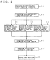
- Fig. 2 is a flowchart illustrating an embodiment of a method of estimating layout area using the layout-area estimating means 11 according to the present invention.
- the method includes processing S1 for inputting connection information relating to a logic circuit, processing S2 for allocating the logic stage count of each logic cell from the entered connection information; processing S3 for calculating, for each logic stage count, a variance in the overall number of input pins in the connection information; processing S4 for calculating a parameter relating to the difference between a number of logic stages (logic stage count) of an output pin and a number of logic stage (logic stage count) of an input pin, wherein these input and output pins are connected at the same node in the connection information, processing S5 for calculating a connected-pin parameter from the overall number of connected pins for each logic cell in the connection information, and processing S6 for obtaining layout area from the variance, the parameter relating to the difference between the logic stage count of an output pin and the logic stage count of an input pin, and the connected-pin parameter.
- the means 111, 112, 113, 114, 115 and 116 in Fig. 1 correspond to the processing steps S1, S2, S3, S4, S5, S5 and S7.
- Fig. 1 is a flowchart of the means for allocating the number of logic stages of logic cells
- Fig. 4 which is a flowchart of the means for calculating the variance in number of input pins by logic stage count
- Fig. 5 which is a flowchart of the means for calculating the difference between the logic stage count of an input pin and the logic stage count of an output pin
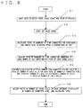
- Fig. 6 which is a flowchart of the calculation means for calculating the parameter relating to the overall number of connected pins.
- the allocation means (processing) (112 in Fig. 1 and S2 in Fig. 2) for allocating the logic stage counts of logic cells extracts (step A1 in Fig.3) a combination of data representing node name, pin attribute and logic cell name from connection information that has been entered by the logic circuit connection-information input means (processing) (111 in Fig.1 and S1 in Fig.2) and retrieves node names, which correspond to external input pins, in regard to input pins of each of the logic cell to which a retrieved input pin belongs and then retrieves the input pins of other logic cells connected to the node name of the output pin of this logic cell (step A3 in Fig. 3).
- the allocation means provisionally adopts, as a first stage of a logic stage count, a logic cell to which a retrieved input pin belongs and then retrieves the input pins of other logic cells connected to the node name of the output pin of this logic cell (step A3 in Fig. 3).
- the allocation means provisionally adopts a value, which is obtained by adding 1 to the logic stage count of an output pin, as the logic stage count of a logic cell to which a newly retrieved input pin belongs, and then retrieves, in regard to input pins of each of the logic cells, the node name of an output pin of the logic cell for which the logic stage count has been newly decided (step A4 in Fig. 3).
- the allocation means repeats the above-described operation until all node names of retrieved output pins of logic cells become external output pins, i.e., until these output pins are no longer connected to input pins of a logic cell (step A5 in Fig. 3). Multiple-input logic cells are retrieved redundantly (duplicatedly). Therefore, in a case where the same logic cell name spans each of (i.e., a plurality of) the logic stage counts, the maximum logic stage count is allocated as the final logic stage count of this logic cell.
- the allocation means creates, in regard to all pins, data obtained by combining node name, pin attribute (in, out), logic cell name and number of logic stages (step A6 in Fig. 3).
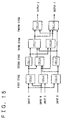
- Fig. 7 is a block diagram showing an example of a circuit having a complicated (irregular) signal connection relationship
- Fig. 8 is a diagram showing an example of data to which logic stage counts have been allocated.
- the allocation means 112 (processing) (112 in Fig. 1 and S2 in Fig.
- connection information concerning a logic circuit having a complicated signal connection relationship
- the logic stage count of this logic cell is finalized (i.e., is no longer provisional).
- the logic cell name of node name A whose pin attribute is "extin” is PIN A and the number of logic stages (the stage count) is 0.
- the logic cell name CELL 1 to which the pin attribute "in” of the pin connected to node A belongs is provisionally adopted as being the first stage of the number of logic stages, this cell has only one input. Accordingly, retrieval ends here and the fact that this is the first stage of the number of logic stages is finalized.
- CELL 2 is the first stage of the logic stage count.
- the remaining cells CELL 3, CELL 5, CELL 6, CELL 7 and CELL 8 have a plurality of inputs and, hence, retrieval is not yet finished.
- the logic stage counts therefore, are still provisional.
- logic cells directly connected to the logic cells CELL 1 and CELL 2, whose logic stage counts have been finalized, are retrieved.
- Input pins (pin attribute "in”) of other logic cells connected to the node name N1 of the pin attribute "out” of the output pin of CELL 1 are retrieved (step A3 in Fig. 3).
- CELL 4 also has two inputs and these are N1 and N2; hence, the fact that this is the second stage of the logic stage count is finalized.
- CELL 10 has three inputs, among which two have not yet been retrieved. Accordingly, it is provisionally decided that the logic stage count is two.
- CELL 5 has two inputs and these are N4 and input C; hence, retrieval ends here and the fact that this is the third stage of the logic stage count is finalized.
- CELL 6 has three inputs and these are N3, N4 and input C for which the logic stage counts have been finalized; hence, the fact that CELL 6 also is the third logic stage of the logic stage count is finalized.
- CELL 7 and CELL 8 also are the third stage of the logic stage count is finalized.
- CELL 9 has two inputs and these are N5 and N8; hence, retrieval ends here and the fact that this is the fourth stage of the logic stage count is finalized.
- CELL 10 has three inputs and these are N6, N7 and N2 for which the logic stage counts have been finalized; hence, the fact that CELL 10 also is the fourth logic stage of the logic stage count is finalized.
- the node names E and F of the output pins "out" of logic cells CELL 9 and CELL 10 for which the logic stage count has been decided anew are connected to external output pins, namely pins whose pin attributes are "extout", the logic cell names whereof are PIN E and PIN F.
- Fig. 8 illustrates that this logic stage count has been allocated to the data representing node name, pin attribute and logic cell name.
- the variance calculation means (processing) (113 in Fig. 1 and S3 in Fig. 2) for calculating a variance in overall number of input pins by logic stage count receives as an input (step B1 in Fig. 4) the data to which the logic stage counts shown in Fig. 8 have been allocated and sorts data, which has been collected into a single set, by each of the logic stage counts 0, 1, 2, 3 and 4 (step B2 in Fig. 4).
- data to which the logic stage counts shown in Fig. 8 have been allocated is accepted as an input, the data is sorted by the logic stage count, the number of input pins is totalized for each logic stage count, the ratios of the numbers of input pins are calculated, a variance in the ratios of the numbers of input pins with respect to the logic stage counts is calculated, and the calculated variance is adopted as a parameter representing the complexity of the signal connection relationship.
- the parameter calculation means (processing) (114 in Fig. 1 and step S4 in Fig. 2) for calculating the difference between logic stage count of output pins and the logic stage count of input pins accepts as an input the data to which the logic stage counts shown in Fig. 8 have been allocated and sorts the data by node name.
- the parameter calculation means 114 calculates the difference between the logic stage count of the logic cells to which the output pin belongs and the logic stage count of the logic cells to which the input pin belongs. This difference between the logic stage counts is referred to as the "stage-count difference”.
- At least one input pin of CELL 3 of the second stage is connected to the external input pin B by being passed through the first stage, and therefore the stage-count difference is two.
- the total of the number of input pins relating to this stage-count difference of two is one.
- At least one input pin of CELL 5, CELL 6, CELL 7, CELL 8 of the third stage is connected to the external input pins C, D or to the output pin of the stage before last, and therefore the stage-count difference is three.
- the total of the number of input pins relating to this stage-count difference of three is six.
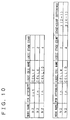
- Fig. 10 shows an example of the calculation of stage-count differences.
- node N2 Take node N2 as an example.
- Fig. 11 illustrates an example of calculation of the stage-count difference parameter between input and output pins.
- the parameter calculation means (115 in Fig. 1, step S5 in Fig. 2) for calculating the overall number of connected pins of each logic cell accepts as an input the data to which the logic stage counts have been allocated (step D1 in Fig. 6) and sorts the data by node name (step D2 in Fig. 6).
- the parameter calculation means 115 calculates the total of the number of connected pins on a per-node basis and creates data in which this total is diminished (subtracted) by one (its own pin) (step D3 in Fig. 6).
- the parameter calculation means 115 retrieves the above-described data in regard to the node names of all input/output pins of a logic cell and sums the data to calculate the total of the number of pins connected to one logic cell.
- the parameter calculation means 115 performs classification by the total of the number of connected pins per logic cell, divides this total of the number of connected pins into several intervals, totalizes the number of logic cells in each interval and calculates a value (referred to as the "ratio of the number of logic cells" below) obtained by dividing the number of logic cells of each interval by the overall number of logic cells (step D5 in Fig. 6).
- the ratio of the number of logic cells of each interval classified by number of connected pins is weighted in accordance with an increase in the number of connected pins, the resulting ratios are totaled and the total is adopted as a parameter representing the complexity of the signal connection relationship.
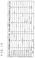
- FIG. 12 illustrates an example of calculation of number of connected pins.
- the data of Fig. 8 to which the logic stage counts have been allocated is accepted as an input and the data is sorted by node name.
- CELL 3 as shown in Fig. 12 (a), three pins, namely "out” of CELL 1, "in” of CELL 4 and its (CELL 3) own pin “in”, are connected to node N1, which is one input, while two pins, namely the B pin and its own pin "in”, are connected to node B, which is the other input of CELL 3.
- the above-mentioned data is retrieved in regard to the node names of all input/output pins of all logic cells and the data is summed to calculate the total of the number of pins connected to one logic cell.
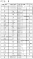
- Fig. 13 shows number of pins connected to one logic cell, as well as number of logic cells classified by the total of the number of connected pins.
- the total of the number of connected pins inclusive of external input/output pins connected for each logic cell is 68. If this is sorted by overall number of connected pins, the number of logic cells with regard to the overall numbers of connected pins 3 to 11 will be ten.
- classification is performed by the total of the number of connected pins per logic cell, the total of the number of connected pins is divided into several intervals (or sections) and the number of logic cells is totalized for each interval.
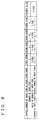
- Fig. 14 is a diagram showing an example of calculation of a parameter relating to the overall number of connected pins of each logic cell. After the number of logic cells is totalized for each interval, as described above, a value (referred to as the "ratio of the number of logic cells" below) obtained by dividing the number of logic cells for each interval by the overall number of logic cells is calculated.
- the ratios of the numbers of logic cells up to 11 as the overall number of connected pins are obtained in similar fashion.
- the ratio of the number of logic cells of each interval classified by number of connected pins is weighted in accordance with an increase in the number of connected pins (here the weighting is changed, e.g., in increments of 0.1 for each increase in the overall number of connected pins). For example, for three as the overall number of connected pins, the ratio 0.20 of the number of logic cells is weighted by 0.3 to give 0.06; for four as the overall number of connected pins, the ratio 0.00 of the number of logic cells is weighted by 0.3 to give 0.00. Values are obtained in similar fashion by weighting the ratios of the numbers of logic cells for overall numbers of connected pins up to 11. When this is done, the total of the values after weighting becomes 0.68.
- the total of the number of connected pins is calculated for each node and data in which this total is diminished by one (its own pin) is created.
- This data is retrieved in regard to the node names of all input/output pins of a logic cell and the data is summed to calculate the total of the number of pins connected to one logic cell, this total is classified by the total of the number of connected pins per logic cell, the number of logic cells is totalized for each number of connected pins and the ratio of the number of logic cells is calculated.
- This ratio of number of logic cells classified by number of connected pins is weighted in accordance with an increase in the number of connected pins, the resulting ratios are totaled and the total is adopted as a parameter representing the complexity of the signal connection relationship.
- the layout-area estimating means (processing) (11 in Fig. 1, steps S6, S7 in Fig. 2) calculates the layout area by substituting, into an already determined calculation equation for estimating layout area, the values calculated by the variance calculation means (processing) (113 in Fig. 1 and S3 in Fig. 2) for calculating a variance in the overall number of input pins by logic stage count, the parameter calculation means (processing) (114 in Fig. 1 and step S4 in Fig. 2) for calculating the difference between logic stage counts of output pins and input pins, and the parameter calculation means (processing) (115 in Fig. 1, step S5 in Fig. 2) for calculating the overall number of connected pins of each logic cell.
- a relation with respect to a layout area for which layout and wiring has been completed is calculated by means separate from the CAD apparatus using, as functions, the variance in overall number of input pins classified by number of logic stages, the parameter relating to the stage-count difference between output and input pins and the parameter relating to the overall number of connected pins of each logic cell.
- the layout area and the equation for calculation thereof change if the series or process differ. If the series and process can be specified, therefore, it will be possible to calculate layout area from parameters calculated on the basis of past performance. As a guide, more complicated circuits require more area than simple circuits. Though the evaluation method is the same as the conventional technique based upon cell-use rate and number of pin pairs, the complexity of the circuit is quantified, thereby making possible an estimation that is more precise than that of the prior art.
- the layout-area estimating means (processing) (11 in Fig. 1 and S7 in Fig. 2) estimates layout area by substituting, into a layout-area estimating calculation determined beforehand by the conventional technique, The values calculated using the variance calculation means 113 for calculating a variance in overall number of input pins by logic stage count, the parameter calculation means 114 for calculating the difference between the logic stage count of output pins and the logic stage count of input pins and the parameter calculation means 115 for calculating the parameter of the overall number of connected pins of each logic cell.
- the optimum chip size is selected based upon the estimated layout area, and layout and wiring are implemented using the automatic layout tool.
- Fig. 15 showing an example of a logic circuit for which the signal connection relationship is simple
- Fig. 16 showing an example of comparison between number of cells used and number of input pins
- Fig. 17 showing an example of a comparison between number of pin pairs and overall area of logic cells used in estimating layout area according to the prior art.
- the values are as illustrated. Since no difference can be recognized between the simple circuit and the complicated circuit in terms of the values shown according to the conventional layout estimation method, it can only be judged that the layout areas are the same.
- Fig. 18 shows an example, to which the present invention has been applied, of a comparison between layout estimation of a complicated circuit and that of a simple circuit
- the complicated circuit has a larger variance value, a larger stage-count difference and a larger number of connections.
- the complicated circuit requires that the layout area be estimated to be larger than that of the simple circuit.
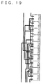
- Fig. 19 showing an example of the layout of a complicated (irregular) circuit, it will be understood that a maximum of seven wiring regions are necessary if the cells are arrayed in one row and wiring is led out from the cells.
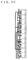
- Fig. 20 shows an example of the layout of a simple (regular) circuit. It will be appreciated that a maximum of five wiring regions suffice if the cells are similarly arrayed in one row and wiring is led out from the cells.
- allocation means allocate logic stage counts of respective ones of logic cells, the allocation means creating, from connection information relating to a logic circuit, data obtained by combining node name, pin attribute, logic cell name and logic stage count for each pin of the logic cell; first calculation means calculates a variance in ratios of numbers of input pins to overall number of input pins obtained by logic stage count; second calculation means calculates a parameter relating to a difference between logic stage count of the output pin and logic stage count of the input pin; and third calculation means calculates a parameter relating to overall number of connected pins for each logic cell; wherein layout area is estimated by the first, second and third calculation means.
- a first effect of the present invention is that since layout and wiring can be implemented with the optimum layout area, it is no longer necessary to implement layout and wiring a number of times leaving unwired portions and enlarging the layout area. This makes it possible to suppress an increase in development time.
- a second effect of the present invention is that since layout and wiring is implemented with the minimum necessary layout area, it is possible to hold down increases in development cost.
Landscapes
- Engineering & Computer Science (AREA)
- Computer Hardware Design (AREA)
- Physics & Mathematics (AREA)
- Theoretical Computer Science (AREA)
- Evolutionary Computation (AREA)
- Geometry (AREA)
- General Engineering & Computer Science (AREA)
- General Physics & Mathematics (AREA)
- Design And Manufacture Of Integrated Circuits (AREA)
Applications Claiming Priority (2)
| Application Number | Priority Date | Filing Date | Title |
|---|---|---|---|
| JP10123163A JP3076301B2 (ja) | 1998-05-06 | 1998-05-06 | 半導体集積回路のレイアウト面積見積り方法およびそのcad装置 |
| JP12316398 | 1998-05-06 |
Publications (1)
| Publication Number | Publication Date |
|---|---|
| EP0955593A2 true EP0955593A2 (en) | 1999-11-10 |
Family
ID=14853752
Family Applications (1)
| Application Number | Title | Priority Date | Filing Date |
|---|---|---|---|
| EP99108571A Withdrawn EP0955593A2 (en) | 1998-05-06 | 1999-05-06 | Method of estimating layout area of semiconductor integrated circuit, and CAD apparatus therefor |
Country Status (2)
| Country | Link |
|---|---|
| EP (1) | EP0955593A2 (ja) |
| JP (1) | JP3076301B2 (ja) |
Cited By (5)
| Publication number | Priority date | Publication date | Assignee | Title |
|---|---|---|---|---|
| RU2398270C1 (ru) * | 2009-02-11 | 2010-08-27 | Государственное образовательное учреждение высшего профессионального образования Курский государственный технический университет | Устройство поиска нижней оценки размещения в полносвязных матричных системах при однонаправленной передаче информации |
| RU2421804C2 (ru) * | 2009-02-17 | 2011-06-20 | Государстенное образовательное учреждение высшего профессионального образования "Юго-Западный государственный университет" | Устройство для формирования матрицы неполного параллелизма |
| RU2447485C2 (ru) * | 2009-09-11 | 2012-04-10 | Федеральное государственное бюджетное образовательное учреждение высшего профессионального образования "Юго-Западный государственный университет" (ЮЗГУ) | Устройство поиска нижней оценки размещения в матричных системах при двунаправленной передаче информации |
| RU2452005C2 (ru) * | 2009-08-05 | 2012-05-27 | Федеральное государственное бюджетное образовательное учреждение высшего профессионального образования "Юго-Западный государственный университет" (ЮЗГУ) | Устройство поиска нижней оценки размещения в матричных системах при направленной передаче информации |
| CN113962177A (zh) * | 2021-11-10 | 2022-01-21 | 上海安路信息科技股份有限公司 | 布线拥塞预估方法及布线拥塞预估系统 |
-
1998
- 1998-05-06 JP JP10123163A patent/JP3076301B2/ja not_active Expired - Lifetime
-
1999
- 1999-05-06 EP EP99108571A patent/EP0955593A2/en not_active Withdrawn
Cited By (5)
| Publication number | Priority date | Publication date | Assignee | Title |
|---|---|---|---|---|
| RU2398270C1 (ru) * | 2009-02-11 | 2010-08-27 | Государственное образовательное учреждение высшего профессионального образования Курский государственный технический университет | Устройство поиска нижней оценки размещения в полносвязных матричных системах при однонаправленной передаче информации |
| RU2421804C2 (ru) * | 2009-02-17 | 2011-06-20 | Государстенное образовательное учреждение высшего профессионального образования "Юго-Западный государственный университет" | Устройство для формирования матрицы неполного параллелизма |
| RU2452005C2 (ru) * | 2009-08-05 | 2012-05-27 | Федеральное государственное бюджетное образовательное учреждение высшего профессионального образования "Юго-Западный государственный университет" (ЮЗГУ) | Устройство поиска нижней оценки размещения в матричных системах при направленной передаче информации |
| RU2447485C2 (ru) * | 2009-09-11 | 2012-04-10 | Федеральное государственное бюджетное образовательное учреждение высшего профессионального образования "Юго-Западный государственный университет" (ЮЗГУ) | Устройство поиска нижней оценки размещения в матричных системах при двунаправленной передаче информации |
| CN113962177A (zh) * | 2021-11-10 | 2022-01-21 | 上海安路信息科技股份有限公司 | 布线拥塞预估方法及布线拥塞预估系统 |
Also Published As
| Publication number | Publication date |
|---|---|
| JP3076301B2 (ja) | 2000-08-14 |
| JPH11316773A (ja) | 1999-11-16 |
Similar Documents
| Publication | Publication Date | Title |
|---|---|---|
| JP3032224B2 (ja) | 半導体集積回路の論理セル配置方法 | |
| JP3548070B2 (ja) | 多端子ネットを自動的に発生する方法及び装置並びに多端子ネット自動発生方法を実行するためのプログラムを記憶したプログラム記憶媒体 | |
| EP1983551A1 (en) | Semiconductor production system | |
| US5550714A (en) | Schematic generator and schematic generating method | |
| EP0170501A2 (en) | Method for logic design of integrated circuit | |
| EP0955593A2 (en) | Method of estimating layout area of semiconductor integrated circuit, and CAD apparatus therefor | |
| US7380228B2 (en) | Method of associating timing violations with critical structures in an integrated circuit design | |
| US7131085B2 (en) | Distributed BDD reordering | |
| US20010049814A1 (en) | Automatic logic design supporting method and apparatus | |
| US6195787B1 (en) | Layout designing method for semiconductor integrated circuits | |
| Behjat et al. | Integer linear programming models for global routing | |
| US6000038A (en) | Parallel processing of Integrated circuit pin arrival times | |
| Kao et al. | Cross point assignment with global rerouting for general-architecture designs | |
| US20090019404A1 (en) | Method for calculating difficulty level of routing in netlist | |
| CN119294328A (zh) | 一种基于数据流规划的fpga布局方法、存储介质和电子设备 | |
| JP3193167B2 (ja) | 論理合成システム | |
| US20060190890A1 (en) | Cell instance generating method | |
| US6367054B1 (en) | Method of generating finite state data for designing a cascade decomposed logic circuit | |
| JPH09102547A (ja) | 回路分割方法 | |
| US6862716B2 (en) | Method for designing interconnects in an LSI | |
| CN117057304A (zh) | 对超导快速单磁通量子电路进行布线的方法和相关产品 | |
| JP2877086B2 (ja) | 回路図面生成装置及び回路図面生成方法 | |
| JPH06244280A (ja) | 自動フロアプランニング装置 | |
| US20010007145A1 (en) | Electronic parts placement method and a computer readable medium having an electronic parts placement program | |
| JP3251792B2 (ja) | 回路ネットワーク分割方法 |
Legal Events
| Date | Code | Title | Description |
|---|---|---|---|
| PUAI | Public reference made under article 153(3) epc to a published international application that has entered the european phase |
Free format text: ORIGINAL CODE: 0009012 |
|
| AK | Designated contracting states |
Kind code of ref document: A2 Designated state(s): AT BE CH CY DE DK ES FI FR GB GR IE IT LI LU MC NL PT SE |
|
| AX | Request for extension of the european patent |
Free format text: AL;LT;LV;MK;RO;SI |
|
| STAA | Information on the status of an ep patent application or granted ep patent |
Free format text: STATUS: THE APPLICATION HAS BEEN WITHDRAWN |
|
| 18W | Application withdrawn |
Effective date: 20030103 |