EP0955708A2 - Laser à émission de surface bleue à cavité verticale - Google Patents
Laser à émission de surface bleue à cavité verticale Download PDFInfo
- Publication number
- EP0955708A2 EP0955708A2 EP99303311A EP99303311A EP0955708A2 EP 0955708 A2 EP0955708 A2 EP 0955708A2 EP 99303311 A EP99303311 A EP 99303311A EP 99303311 A EP99303311 A EP 99303311A EP 0955708 A2 EP0955708 A2 EP 0955708A2
- Authority
- EP
- European Patent Office
- Prior art keywords
- layer
- gallium nitride
- gan
- surface emitting
- emitting laser
- Prior art date
- Legal status (The legal status is an assumption and is not a legal conclusion. Google has not performed a legal analysis and makes no representation as to the accuracy of the status listed.)
- Withdrawn
Links
Images


Classifications
-
- H—ELECTRICITY
- H01—ELECTRIC ELEMENTS
- H01S—DEVICES USING THE PROCESS OF LIGHT AMPLIFICATION BY STIMULATED EMISSION OF RADIATION [LASER] TO AMPLIFY OR GENERATE LIGHT; DEVICES USING STIMULATED EMISSION OF ELECTROMAGNETIC RADIATION IN WAVE RANGES OTHER THAN OPTICAL
- H01S5/00—Semiconductor lasers
- H01S5/30—Structure or shape of the active region; Materials used for the active region
- H01S5/34—Structure or shape of the active region; Materials used for the active region comprising quantum well or superlattice structures, e.g. single quantum well [SQW] lasers, multiple quantum well [MQW] lasers or graded index separate confinement heterostructure [GRINSCH] lasers
- H01S5/343—Structure or shape of the active region; Materials used for the active region comprising quantum well or superlattice structures, e.g. single quantum well [SQW] lasers, multiple quantum well [MQW] lasers or graded index separate confinement heterostructure [GRINSCH] lasers in AIIIBV compounds, e.g. AlGaAs-laser, InP-based laser
- H01S5/34333—Structure or shape of the active region; Materials used for the active region comprising quantum well or superlattice structures, e.g. single quantum well [SQW] lasers, multiple quantum well [MQW] lasers or graded index separate confinement heterostructure [GRINSCH] lasers in AIIIBV compounds, e.g. AlGaAs-laser, InP-based laser with a well layer based on Ga(In)N or Ga(In)P, e.g. blue laser
-
- B—PERFORMING OPERATIONS; TRANSPORTING
- B82—NANOTECHNOLOGY
- B82Y—SPECIFIC USES OR APPLICATIONS OF NANOSTRUCTURES; MEASUREMENT OR ANALYSIS OF NANOSTRUCTURES; MANUFACTURE OR TREATMENT OF NANOSTRUCTURES
- B82Y20/00—Nanooptics, e.g. quantum optics or photonic crystals
-
- H—ELECTRICITY
- H01—ELECTRIC ELEMENTS
- H01S—DEVICES USING THE PROCESS OF LIGHT AMPLIFICATION BY STIMULATED EMISSION OF RADIATION [LASER] TO AMPLIFY OR GENERATE LIGHT; DEVICES USING STIMULATED EMISSION OF ELECTROMAGNETIC RADIATION IN WAVE RANGES OTHER THAN OPTICAL
- H01S2304/00—Special growth methods for semiconductor lasers
-
- H—ELECTRICITY
- H01—ELECTRIC ELEMENTS
- H01S—DEVICES USING THE PROCESS OF LIGHT AMPLIFICATION BY STIMULATED EMISSION OF RADIATION [LASER] TO AMPLIFY OR GENERATE LIGHT; DEVICES USING STIMULATED EMISSION OF ELECTROMAGNETIC RADIATION IN WAVE RANGES OTHER THAN OPTICAL
- H01S2304/00—Special growth methods for semiconductor lasers
- H01S2304/04—MOCVD or MOVPE
-
- H—ELECTRICITY
- H01—ELECTRIC ELEMENTS
- H01S—DEVICES USING THE PROCESS OF LIGHT AMPLIFICATION BY STIMULATED EMISSION OF RADIATION [LASER] TO AMPLIFY OR GENERATE LIGHT; DEVICES USING STIMULATED EMISSION OF ELECTROMAGNETIC RADIATION IN WAVE RANGES OTHER THAN OPTICAL
- H01S5/00—Semiconductor lasers
- H01S5/02—Structural details or components not essential to laser action
- H01S5/0206—Substrates, e.g. growth, shape, material, removal or bonding
- H01S5/0207—Substrates having a special shape
-
- H—ELECTRICITY
- H01—ELECTRIC ELEMENTS
- H01S—DEVICES USING THE PROCESS OF LIGHT AMPLIFICATION BY STIMULATED EMISSION OF RADIATION [LASER] TO AMPLIFY OR GENERATE LIGHT; DEVICES USING STIMULATED EMISSION OF ELECTROMAGNETIC RADIATION IN WAVE RANGES OTHER THAN OPTICAL
- H01S5/00—Semiconductor lasers
- H01S5/02—Structural details or components not essential to laser action
- H01S5/0206—Substrates, e.g. growth, shape, material, removal or bonding
- H01S5/0213—Sapphire, quartz or diamond based substrates
-
- H—ELECTRICITY
- H01—ELECTRIC ELEMENTS
- H01S—DEVICES USING THE PROCESS OF LIGHT AMPLIFICATION BY STIMULATED EMISSION OF RADIATION [LASER] TO AMPLIFY OR GENERATE LIGHT; DEVICES USING STIMULATED EMISSION OF ELECTROMAGNETIC RADIATION IN WAVE RANGES OTHER THAN OPTICAL
- H01S5/00—Semiconductor lasers
- H01S5/04—Processes or apparatus for excitation, e.g. pumping, e.g. by electron beams
- H01S5/042—Electrical excitation ; Circuits therefor
- H01S5/0425—Electrodes, e.g. characterised by the structure
- H01S5/04256—Electrodes, e.g. characterised by the structure characterised by the configuration
-
- H—ELECTRICITY
- H01—ELECTRIC ELEMENTS
- H01S—DEVICES USING THE PROCESS OF LIGHT AMPLIFICATION BY STIMULATED EMISSION OF RADIATION [LASER] TO AMPLIFY OR GENERATE LIGHT; DEVICES USING STIMULATED EMISSION OF ELECTROMAGNETIC RADIATION IN WAVE RANGES OTHER THAN OPTICAL
- H01S5/00—Semiconductor lasers
- H01S5/04—Processes or apparatus for excitation, e.g. pumping, e.g. by electron beams
- H01S5/042—Electrical excitation ; Circuits therefor
- H01S5/0425—Electrodes, e.g. characterised by the structure
- H01S5/04256—Electrodes, e.g. characterised by the structure characterised by the configuration
- H01S5/04257—Electrodes, e.g. characterised by the structure characterised by the configuration having positive and negative electrodes on the same side of the substrate
-
- H—ELECTRICITY
- H01—ELECTRIC ELEMENTS
- H01S—DEVICES USING THE PROCESS OF LIGHT AMPLIFICATION BY STIMULATED EMISSION OF RADIATION [LASER] TO AMPLIFY OR GENERATE LIGHT; DEVICES USING STIMULATED EMISSION OF ELECTROMAGNETIC RADIATION IN WAVE RANGES OTHER THAN OPTICAL
- H01S5/00—Semiconductor lasers
- H01S5/10—Construction or shape of the optical resonator, e.g. extended or external cavity, coupled cavities, bent-guide, varying width, thickness or composition of the active region
- H01S5/18—Surface-emitting [SE] lasers, e.g. having both horizontal and vertical cavities
- H01S5/183—Surface-emitting [SE] lasers, e.g. having both horizontal and vertical cavities having only vertical cavities, e.g. vertical cavity surface-emitting lasers [VCSEL]
- H01S5/18341—Intra-cavity contacts
-
- H—ELECTRICITY
- H01—ELECTRIC ELEMENTS
- H01S—DEVICES USING THE PROCESS OF LIGHT AMPLIFICATION BY STIMULATED EMISSION OF RADIATION [LASER] TO AMPLIFY OR GENERATE LIGHT; DEVICES USING STIMULATED EMISSION OF ELECTROMAGNETIC RADIATION IN WAVE RANGES OTHER THAN OPTICAL
- H01S5/00—Semiconductor lasers
- H01S5/10—Construction or shape of the optical resonator, e.g. extended or external cavity, coupled cavities, bent-guide, varying width, thickness or composition of the active region
- H01S5/18—Surface-emitting [SE] lasers, e.g. having both horizontal and vertical cavities
- H01S5/183—Surface-emitting [SE] lasers, e.g. having both horizontal and vertical cavities having only vertical cavities, e.g. vertical cavity surface-emitting lasers [VCSEL]
- H01S5/18361—Structure of the reflectors, e.g. hybrid mirrors
- H01S5/18369—Structure of the reflectors, e.g. hybrid mirrors based on dielectric materials
Definitions
- This invention relates to a monolithic semiconductor laser structure and, more particularly, to an independently addressable, vertical cavity surface emitting laser (“VCSEL”) in the blue wavelength range.
- VCSEL vertical cavity surface emitting laser
- Monolithic solid state semiconductor lasers are very desirable light sources for high speed laser printing, optical fiber communications and other applications. Recently, there has been an increased interest in vertical cavity surface emitting lasers although edge emitting lasers are currently used in the vast majority of applications.
- a common laser structure is a so-called “edge emitting laser” where light is emitted from the edge of a monolithic structure of semiconductor layers.
- a laser structure is a "VCSEL" where the light is emitted from the surface of the monolithic structure of semiconductor layers.
- VCSEL edge emitting lasers produce a beam with a large angular divergence, making efficient collection of the emitted beam more difficult.
- a VCSEL emits light normal to the surface of the wafer.
- Prior art quantum well vertical cavity surface emitting lasers can emit light in the wavelength range of about 600 to 650 nanometers (the red range) or in the range above 650 nanometers (the infrared range). However, there are important applications for laser devices that emit light in the wavelength range significantly around 400 nanometers (the blue range).
- GaN gallium nitride and its alloys with indium and aluminum are used as the semiconductor layers in the blue laser structure.
- GaN itself cannot be used as a practical substrate.
- the problem is the lack of a suitable, lattice-matched substrate for the GaN semiconductor layers. Without a substrate with a lattice constant close to that of GaN, there will be a high density of extended defects in the nitride layers.
- An active layer of GaN and its alloys on a poorly lattice matched substrate will emit coherent blue light poorly and inefficiently, if at all.
- Sapphire Al 2 O 3
- GaN gallium-nitride
- An approximate epitaxial relationship between a sapphire substrate and a GaN alloy semiconductor laser structure can be obtained by matching specific crystallographic directions. However, a lattice mismatch of approximately 15 percent results from such a semiconductor structure.
- the present invention provides an independently addressable, vertical cavity surface emitting laser ("VCSEL") in the blue wavelength range of 390 to 430 nanometers.
- VCSEL vertical cavity surface emitting laser
- the gallium nitride-based laser structure is grown by selective area epitaxy and lateral mask overgrowth. By appropriate patterning of a dielectric mask on the gallium nitride layer on a sapphire substrate, areas in a second gallium nitride layer can have a low defect density upon which the remainder of the laser structure can be formed.
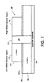
- Figure 1 illustrates a gallium nitride (GaN) crystal structure 100 for use in a vertical cavity surface emitting laser in accordance with the present invention.
- GaN gallium nitride
- the structure 100 comprises a sapphire (Al 2 O 3 ) substrate 102 upon which is first grown a n-gallium nitride (n-GaN) base layer 104 using an epitaxial deposition process known as metal-organic chemical vapor deposition (“MOCVD”) as is well known in the art.
- MOCVD metal-organic chemical vapor deposition
- a 200 nm thick dielectric film 106 of silicon dioxide (SiO 2 ) is then deposited on the GaN base layer 104 by plasma-enhanced chemical vapor deposition ("PECVD") or by electron beam evaporation.
- PECVD plasma-enhanced chemical vapor deposition
- the dielectric film 106 is then patterned by using standard photolithographic procedures and etching with hydrofluoric acid (HF).
- a thin linear stripe 108 is etched down in the dielectric film 106 to expose the surface of the GaN base layer 104.
- a second n-gallium nitride (n-GaN) layer 110 of 4 ⁇ m thickness with a lateral width of 16 ⁇ m is then grown laterally starting at the thin exposed stripe 108.
- the GaN layer 110 grows laterally above the dielectric film 106 under high temperature and high ammonia flow, as described in Kapolnek et al., "Anistropic epitaxial lateral growth in GaN selective area epitaxy", Applied Physics Letters, vol. 71(9), 1 September 1997, pp. 1204-1206.
- the layer 110 starts selectively only in the exposed GaN area 108, but not on the top surface of the SiO 2 layer 106. As the layer 110 gets thicker, the layer starts to laterally overgrow the SiO 2 layer 106. Since this laterally overgrown material is attached to the lower GaN layer 104 only on one side, it will grow without strain and, therefore, without dislocations. The second GaN layer 110 will be laterally overgrown over the GaN base layer 104 and above the dielectric film 106 on each side of the stripe 108.
- the GaN layer 110 consists of three sections: a first or end section 112 atop one portion of the dielectric film 106, a second or middle section 114 atop the exposed stripe 108 of the GaN base layer 104 and a third or end section 116 atop another portion of the dielectric film 106.
- the two end portions 112 and 116 since they are deposited on top of the dielectric film 106 are in the low defect density regions of the GaN layer 110.
- the middle section 114 since it is deposited on the other first GaN base layer 104 is in the high defect density regions of the second GaN layer 110.
- the laser heterostructures will be grown by epitaxy upon one section of the lateral overgrowth of the GaN layer 110 upon the dielectric film 106 and the linear stripe 108 of the GaN base layer 104.
- the subsequent growth of GaN based laser heterostructures over a patterned substrate 110 leads to low defect crystal areas 112 and 116 away from the high defect crystal area 114.
- the dielectric film 106 deposited on the GaN base layer 104 can, in the alternative, be silicon nitride (SiN x ) or silicon oxide nitride (SiON).
- the blue vertical cavity surface emitting laser "VCSEL" semiconductor structure 200 of Figure 2 is fabricated in accordance to the present invention.
- the blue VCSEL laser structure 200 comprises a sapphire (Al 2 O 3 ) substrate 202 upon which is first grown a n-gallium nitride (n-GaN) base layer 204 using an epitaxial deposition process known as metal-organic chemical vapor deposition (“MOCVD”) as is well known in the art.
- MOCVD metal-organic chemical vapor deposition
- a narrow bandwidth distributed Bragg reflector (“DBR") 206 of approximately 8 to 12 alternating layers of dielectric film materials such as n-SiO 2 and n-TiO 2 is then deposited on the GaN base layer 204 by plasma-enhanced chemical vapor deposition ("PECVD”) or by electron beam evaporation.
- PECVD plasma-enhanced chemical vapor deposition
- the lower n-DBR 206 may be a 10 quarter-wave stack at the light emission wavelength in the blue spectrum for the laser structure 200.
- the thicknesses of the n-SiO 2 and n-TiO 2 layers are a quarter of the wavelength which is nominally 69 nm in the SiO 2 and nominally 45 nm in the TiO 2 .
- the lower DBR 206 will be approximately 1.14 microns thick.
- the dielectric film DBR 206 is then patterned by using standard photolithographic procedures and etching with hydrofluoric acid (HF).
- HF hydrofluoric acid
- a thin linear stripe 208 is etched down in the dielectric film DBR 206 to expose the surface of the GaN base layer 204.
- a second n-gallium nitride (n-GaN) layer 210 of 4 ⁇ m thickness with a lateral width of 16 ⁇ m is then selectively deposited on the dielectric film DBR 206 and the thin exposed stripe 208 of the GaN base layer 204.
- the second GaN layer 210 will be laterally overgrown over the GaN base layer 204 and above the dielectric film 206 on each side of the stripe 208.
- the GaN layer 210 consists of three sections: a first or end section 212 atop one portion of the dielectric film DBR 206, a second or middle section 214 atop the exposed stripe 208 of the GaN base layer 204 and a third or end section 216 atop another portion of the dielectric film DBR 206.
- the two end portions 212 and 216 since they are deposited on top of the dielectric film 206 are in the low defect density regions of the GaN layer 210.
- the middle section 214 since it is deposited on the GaN base layer 204 is in the high defect density regions of the second GaN layer 210.
- the laser heterostructure is then deposited on the GaN layer 210.
- n-Al 0.08 Ga 0.92 N aluminum gallium nitride cladding layer 218 is deposited on the GaN layer 210.
- the n-Al 0.08 Ga 0.92 N aluminum gallium nitride cladding layer 218 has a thickness of 0.5 ⁇ m and is silicon doped to a concentration of 5 x 10 17 cm -3 .
- a first lower n-GaN confinement layer 220 is deposited upon the lower cladding layer 218.
- the n-GaN confinement layer 220 has a thickness of 100 nanometers and is silicon doped to a concentration of 10 18 cm -3 .
- An In 0.15 Ga 0.85 N/GaN multiple quantum well active layer 222 is deposited on the confinement layer 220.
- the In 0.15 Ga 0.85 N/GaN multiple quantum well active layer 222 is undoped and has a thickness of 120 nm.
- a second upper p-GaN confinement layer 224 is deposited upon the multiple quantum well active layer 222.
- the p-GaN confinement layer 224 has a thickness of 100 nanometers and is magnesium doped to a concentration of 10 18 cm -3 .
- An upper p-Al 0.08 Ga 0.92 N aluminum gallium nitride cladding layer 226 is deposited on the confinement layer 224.
- the p-Al 0.08 Ga 0.92 N aluminum gallium nitride cladding layer 226 has a thickness of 0.5 ⁇ m and is magnesium doped to a concentration of 5 x 10 17 cm -3 .
- a third p-GaN contact layer 228 is deposited on the upper cladding layer 226.
- the contract layer 228 has a thickness of 120 nanometers and is magnesium doped to a concentration of 5 x 10 17 cm -3 .
- the multiple quantum well layer 222 forms the active region for emission of light in the blue wavelengths of 390 to 430 nanometers.
- the laser heterostructure 200 is formed of gallium nitride semiconductor layers and its alloys with aluminum and/or indium.
- Dry etching of the laser structure 200 will remove portions of epitaxial layers above the first section 212 above the dielectric film 206 and the second section 214 above the GaN layer 210, leaving a mesa laser structure 230 above the third section 216 above the dielectric film 206.
- a small portion (not shown) of the second section 214 may remain attached to the side of the mesa to provide insulation and isolation. Additionally, this etching step can be used to remove any polycrystalline material that may collect on the dielectric mask during AlGaN growth.
- An annular p-contact 232 of Cr-Au or Ti-Pt-Au is formed by metal evaporation on the contact layer 228.
- an InGaN contact layer (not shown) can be deposited on the contact layer 228 first, followed by the formation of the p-contact 232.
- the upper p-DBR 234 is formed on the surface of the contact layer 228.
- the narrow bandwidth distributed Bragg reflector (“DBR”) 234 consists of approximately 8 to 12 alternating layers of dielectric film materials such as n-SiO 2 and n-TiO 2 which are deposited on the GaN contact layer 228 by plasma-enhanced chemical vapor deposition (“PECVD”) or by electron beam evaporation.
- PECVD plasma-enhanced chemical vapor deposition
- the upper p-DBR 234 may be a 10 quarter-wave stack at the light emission wavelength in the blue spectrum for the laser structure 230.
- the thicknesses of the n-SiO 2 and n-TiO 2 layers are a quarter of the wavelength which is nominally 69 nm in the SiO 2 and nominally 45 nm in the TiO 2 .
- the upper DBR 234 will be approximately 1.14 microns thick.
- An air-bridge 236 of Cr-Au or Ti-Pt-Au connects the annular p-contact 232 to a much larger contact pad 238 on the surface of the sapphire substrate 202.
- a n-contact 240 of Cr-Au or Ti-Pt-Au is formed by metal evaporation on the first or end section 212 of the GaN layer 210.
- the vertical nature of the laser structure 230 upon the third section 216 of the GaN layer 210 provides lateral optical and electrical confinement in the laser.
- the active region will emit light through the surface of the laser structure 230 through either the lower DBR 206 or through the upper DBR 236.
- the dielectric film materials used in the DBRs can be alternating layers of SiN and SiO 2 or other suitable dielectric materials.
Landscapes
- Physics & Mathematics (AREA)
- Nanotechnology (AREA)
- Engineering & Computer Science (AREA)
- Chemical & Material Sciences (AREA)
- Optics & Photonics (AREA)
- Biophysics (AREA)
- Life Sciences & Earth Sciences (AREA)
- Electromagnetism (AREA)
- General Physics & Mathematics (AREA)
- Crystallography & Structural Chemistry (AREA)
- Condensed Matter Physics & Semiconductors (AREA)
- Semiconductor Lasers (AREA)
- Led Devices (AREA)
Applications Claiming Priority (2)
| Application Number | Priority Date | Filing Date | Title |
|---|---|---|---|
| US09/073,707 US6160833A (en) | 1998-05-06 | 1998-05-06 | Blue vertical cavity surface emitting laser |
| US73707 | 1998-05-06 |
Publications (2)
| Publication Number | Publication Date |
|---|---|
| EP0955708A2 true EP0955708A2 (fr) | 1999-11-10 |
| EP0955708A3 EP0955708A3 (fr) | 2000-07-05 |
Family
ID=22115306
Family Applications (1)
| Application Number | Title | Priority Date | Filing Date |
|---|---|---|---|
| EP99303311A Withdrawn EP0955708A3 (fr) | 1998-05-06 | 1999-04-28 | Laser à émission de surface bleue à cavité verticale |
Country Status (3)
| Country | Link |
|---|---|
| US (1) | US6160833A (fr) |
| EP (1) | EP0955708A3 (fr) |
| JP (1) | JPH11340582A (fr) |
Cited By (3)
| Publication number | Priority date | Publication date | Assignee | Title |
|---|---|---|---|---|
| DE10012869A1 (de) * | 2000-03-16 | 2001-09-27 | Infineon Technologies Ag | Vertikalresonator-Laserdiode mit koplanaren elektrischen Anschlußkontakten |
| US6610144B2 (en) * | 2000-07-21 | 2003-08-26 | The Regents Of The University Of California | Method to reduce the dislocation density in group III-nitride films |
| CN113964252A (zh) * | 2020-07-21 | 2022-01-21 | 苏州晶湛半导体有限公司 | 半导体结构及其制备方法 |
Families Citing this family (195)
| Publication number | Priority date | Publication date | Assignee | Title |
|---|---|---|---|---|
| US6674562B1 (en) | 1994-05-05 | 2004-01-06 | Iridigm Display Corporation | Interferometric modulation of radiation |
| US7550794B2 (en) | 2002-09-20 | 2009-06-23 | Idc, Llc | Micromechanical systems device comprising a displaceable electrode and a charge-trapping layer |
| US7138984B1 (en) | 2001-06-05 | 2006-11-21 | Idc, Llc | Directly laminated touch sensitive screen |
| US7460291B2 (en) | 1994-05-05 | 2008-12-02 | Idc, Llc | Separable modulator |
| US6680792B2 (en) | 1994-05-05 | 2004-01-20 | Iridigm Display Corporation | Interferometric modulation of radiation |
| US7297471B1 (en) | 2003-04-15 | 2007-11-20 | Idc, Llc | Method for manufacturing an array of interferometric modulators |
| US8014059B2 (en) | 1994-05-05 | 2011-09-06 | Qualcomm Mems Technologies, Inc. | System and method for charge control in a MEMS device |
| US7123216B1 (en) | 1994-05-05 | 2006-10-17 | Idc, Llc | Photonic MEMS and structures |
| US7471444B2 (en) | 1996-12-19 | 2008-12-30 | Idc, Llc | Interferometric modulation of radiation |
| US8928967B2 (en) | 1998-04-08 | 2015-01-06 | Qualcomm Mems Technologies, Inc. | Method and device for modulating light |
| US7532377B2 (en) | 1998-04-08 | 2009-05-12 | Idc, Llc | Movable micro-electromechanical device |
| KR100703140B1 (ko) | 1998-04-08 | 2007-04-05 | 이리다임 디스플레이 코포레이션 | 간섭 변조기 및 그 제조 방법 |
| GB9807692D0 (en) | 1998-04-14 | 1998-06-10 | Univ Strathclyde | Optival devices |
| WO2003007049A1 (fr) | 1999-10-05 | 2003-01-23 | Iridigm Display Corporation | Mems et structures photoniques |
| US6611544B1 (en) | 2000-04-11 | 2003-08-26 | E20 Communications, Inc. | Method and apparatus for narrow bandwidth distributed bragg reflector semiconductor lasers |
| JP2001313440A (ja) * | 2000-04-27 | 2001-11-09 | Sony Corp | 窒化物半導体発光素子 |
| US6878958B2 (en) * | 2001-03-26 | 2005-04-12 | Gazillion Bits, Inc. | Vertical cavity surface emitting laser with buried dielectric distributed Bragg reflector |
| US20020163688A1 (en) * | 2001-03-26 | 2002-11-07 | Zuhua Zhu | Optical communications system and vertical cavity surface emitting laser therefor |
| US6784074B2 (en) | 2001-05-09 | 2004-08-31 | Nsc-Nanosemiconductor Gmbh | Defect-free semiconductor templates for epitaxial growth and method of making same |
| US6653166B2 (en) * | 2001-05-09 | 2003-11-25 | Nsc-Nanosemiconductor Gmbh | Semiconductor device and method of making same |
| JP2002334842A (ja) * | 2001-05-10 | 2002-11-22 | Sony Corp | 窒化物半導体装置の製造方法 |
| US7442629B2 (en) | 2004-09-24 | 2008-10-28 | President & Fellows Of Harvard College | Femtosecond laser-induced formation of submicrometer spikes on a semiconductor substrate |
| US7057256B2 (en) | 2001-05-25 | 2006-06-06 | President & Fellows Of Harvard College | Silicon-based visible and near-infrared optoelectric devices |
| JP3876649B2 (ja) * | 2001-06-05 | 2007-02-07 | ソニー株式会社 | 窒化物半導体レーザ及びその製造方法 |
| US6589625B1 (en) | 2001-08-01 | 2003-07-08 | Iridigm Display Corporation | Hermetic seal and method to create the same |
| TW561526B (en) * | 2001-12-21 | 2003-11-11 | Aixtron Ag | Method for depositing III-V semiconductor layers on a non-III-V substrate |
| US6794119B2 (en) | 2002-02-12 | 2004-09-21 | Iridigm Display Corporation | Method for fabricating a structure for a microelectromechanical systems (MEMS) device |
| US6574033B1 (en) | 2002-02-27 | 2003-06-03 | Iridigm Display Corporation | Microelectromechanical systems device and method for fabricating same |
| US7781850B2 (en) | 2002-09-20 | 2010-08-24 | Qualcomm Mems Technologies, Inc. | Controlling electromechanical behavior of structures within a microelectromechanical systems device |
| TW200413810A (en) | 2003-01-29 | 2004-08-01 | Prime View Int Co Ltd | Light interference display panel and its manufacturing method |
| US20060276043A1 (en) * | 2003-03-21 | 2006-12-07 | Johnson Mark A L | Method and systems for single- or multi-period edge definition lithography |
| TW594360B (en) | 2003-04-21 | 2004-06-21 | Prime View Int Corp Ltd | A method for fabricating an interference display cell |
| TW570896B (en) | 2003-05-26 | 2004-01-11 | Prime View Int Co Ltd | A method for fabricating an interference display cell |
| US7221495B2 (en) | 2003-06-24 | 2007-05-22 | Idc Llc | Thin film precursor stack for MEMS manufacturing |
| TWI231865B (en) | 2003-08-26 | 2005-05-01 | Prime View Int Co Ltd | An interference display cell and fabrication method thereof |
| TW593126B (en) | 2003-09-30 | 2004-06-21 | Prime View Int Co Ltd | A structure of a micro electro mechanical system and manufacturing the same |
| US7009215B2 (en) * | 2003-10-24 | 2006-03-07 | General Electric Company | Group III-nitride based resonant cavity light emitting devices fabricated on single crystal gallium nitride substrates |
| US7012726B1 (en) | 2003-11-03 | 2006-03-14 | Idc, Llc | MEMS devices with unreleased thin film components |
| US7161728B2 (en) | 2003-12-09 | 2007-01-09 | Idc, Llc | Area array modulation and lead reduction in interferometric modulators |
| US7142346B2 (en) | 2003-12-09 | 2006-11-28 | Idc, Llc | System and method for addressing a MEMS display |
| US7532194B2 (en) | 2004-02-03 | 2009-05-12 | Idc, Llc | Driver voltage adjuster |
| US7119945B2 (en) | 2004-03-03 | 2006-10-10 | Idc, Llc | Altering temporal response of microelectromechanical elements |
| US7706050B2 (en) | 2004-03-05 | 2010-04-27 | Qualcomm Mems Technologies, Inc. | Integrated modulator illumination |
| US7476327B2 (en) | 2004-05-04 | 2009-01-13 | Idc, Llc | Method of manufacture for microelectromechanical devices |
| US7060895B2 (en) | 2004-05-04 | 2006-06-13 | Idc, Llc | Modifying the electro-mechanical behavior of devices |
| US7164520B2 (en) | 2004-05-12 | 2007-01-16 | Idc, Llc | Packaging for an interferometric modulator |
| US7256922B2 (en) | 2004-07-02 | 2007-08-14 | Idc, Llc | Interferometric modulators with thin film transistors |
| EP1779173A1 (fr) | 2004-07-29 | 2007-05-02 | Idc, Llc | Systeme et procede pour le fonctionnement micro-electromecanique d'un modulateur interferometrique |
| US7560299B2 (en) | 2004-08-27 | 2009-07-14 | Idc, Llc | Systems and methods of actuating MEMS display elements |
| US7889163B2 (en) | 2004-08-27 | 2011-02-15 | Qualcomm Mems Technologies, Inc. | Drive method for MEMS devices |
| US7499208B2 (en) | 2004-08-27 | 2009-03-03 | Udc, Llc | Current mode display driver circuit realization feature |
| US7551159B2 (en) | 2004-08-27 | 2009-06-23 | Idc, Llc | System and method of sensing actuation and release voltages of an interferometric modulator |
| US7515147B2 (en) | 2004-08-27 | 2009-04-07 | Idc, Llc | Staggered column drive circuit systems and methods |
| US7602375B2 (en) | 2004-09-27 | 2009-10-13 | Idc, Llc | Method and system for writing data to MEMS display elements |
| US7701631B2 (en) | 2004-09-27 | 2010-04-20 | Qualcomm Mems Technologies, Inc. | Device having patterned spacers for backplates and method of making the same |
| US7944599B2 (en) | 2004-09-27 | 2011-05-17 | Qualcomm Mems Technologies, Inc. | Electromechanical device with optical function separated from mechanical and electrical function |
| US7684104B2 (en) | 2004-09-27 | 2010-03-23 | Idc, Llc | MEMS using filler material and method |
| US7545550B2 (en) | 2004-09-27 | 2009-06-09 | Idc, Llc | Systems and methods of actuating MEMS display elements |
| US7843410B2 (en) | 2004-09-27 | 2010-11-30 | Qualcomm Mems Technologies, Inc. | Method and device for electrically programmable display |
| US8878825B2 (en) | 2004-09-27 | 2014-11-04 | Qualcomm Mems Technologies, Inc. | System and method for providing a variable refresh rate of an interferometric modulator display |
| US7161730B2 (en) | 2004-09-27 | 2007-01-09 | Idc, Llc | System and method for providing thermal compensation for an interferometric modulator display |
| US7420725B2 (en) | 2004-09-27 | 2008-09-02 | Idc, Llc | Device having a conductive light absorbing mask and method for fabricating same |
| US7554714B2 (en) | 2004-09-27 | 2009-06-30 | Idc, Llc | Device and method for manipulation of thermal response in a modulator |
| US7302157B2 (en) | 2004-09-27 | 2007-11-27 | Idc, Llc | System and method for multi-level brightness in interferometric modulation |
| US7405924B2 (en) | 2004-09-27 | 2008-07-29 | Idc, Llc | System and method for protecting microelectromechanical systems array using structurally reinforced back-plate |
| US7136213B2 (en) | 2004-09-27 | 2006-11-14 | Idc, Llc | Interferometric modulators having charge persistence |
| US7710629B2 (en) | 2004-09-27 | 2010-05-04 | Qualcomm Mems Technologies, Inc. | System and method for display device with reinforcing substance |
| US7372613B2 (en) | 2004-09-27 | 2008-05-13 | Idc, Llc | Method and device for multistate interferometric light modulation |
| US7653371B2 (en) | 2004-09-27 | 2010-01-26 | Qualcomm Mems Technologies, Inc. | Selectable capacitance circuit |
| US7355780B2 (en) | 2004-09-27 | 2008-04-08 | Idc, Llc | System and method of illuminating interferometric modulators using backlighting |
| TW200628833A (en) | 2004-09-27 | 2006-08-16 | Idc Llc | Method and device for multistate interferometric light modulation |
| US7405861B2 (en) | 2004-09-27 | 2008-07-29 | Idc, Llc | Method and device for protecting interferometric modulators from electrostatic discharge |
| US8124434B2 (en) | 2004-09-27 | 2012-02-28 | Qualcomm Mems Technologies, Inc. | Method and system for packaging a display |
| US7583429B2 (en) | 2004-09-27 | 2009-09-01 | Idc, Llc | Ornamental display device |
| US7808703B2 (en) | 2004-09-27 | 2010-10-05 | Qualcomm Mems Technologies, Inc. | System and method for implementation of interferometric modulator displays |
| US7317568B2 (en) | 2004-09-27 | 2008-01-08 | Idc, Llc | System and method of implementation of interferometric modulators for display mirrors |
| US7916103B2 (en) | 2004-09-27 | 2011-03-29 | Qualcomm Mems Technologies, Inc. | System and method for display device with end-of-life phenomena |
| US7349136B2 (en) | 2004-09-27 | 2008-03-25 | Idc, Llc | Method and device for a display having transparent components integrated therein |
| US7368803B2 (en) | 2004-09-27 | 2008-05-06 | Idc, Llc | System and method for protecting microelectromechanical systems array using back-plate with non-flat portion |
| US7626581B2 (en) | 2004-09-27 | 2009-12-01 | Idc, Llc | Device and method for display memory using manipulation of mechanical response |
| US7453579B2 (en) | 2004-09-27 | 2008-11-18 | Idc, Llc | Measurement of the dynamic characteristics of interferometric modulators |
| US7373026B2 (en) | 2004-09-27 | 2008-05-13 | Idc, Llc | MEMS device fabricated on a pre-patterned substrate |
| US7532195B2 (en) | 2004-09-27 | 2009-05-12 | Idc, Llc | Method and system for reducing power consumption in a display |
| US7668415B2 (en) | 2004-09-27 | 2010-02-23 | Qualcomm Mems Technologies, Inc. | Method and device for providing electronic circuitry on a backplate |
| US7893919B2 (en) | 2004-09-27 | 2011-02-22 | Qualcomm Mems Technologies, Inc. | Display region architectures |
| US8008736B2 (en) | 2004-09-27 | 2011-08-30 | Qualcomm Mems Technologies, Inc. | Analog interferometric modulator device |
| US7289259B2 (en) | 2004-09-27 | 2007-10-30 | Idc, Llc | Conductive bus structure for interferometric modulator array |
| US7417735B2 (en) | 2004-09-27 | 2008-08-26 | Idc, Llc | Systems and methods for measuring color and contrast in specular reflective devices |
| US7327510B2 (en) | 2004-09-27 | 2008-02-05 | Idc, Llc | Process for modifying offset voltage characteristics of an interferometric modulator |
| US7813026B2 (en) | 2004-09-27 | 2010-10-12 | Qualcomm Mems Technologies, Inc. | System and method of reducing color shift in a display |
| US7920135B2 (en) | 2004-09-27 | 2011-04-05 | Qualcomm Mems Technologies, Inc. | Method and system for driving a bi-stable display |
| US7359066B2 (en) | 2004-09-27 | 2008-04-15 | Idc, Llc | Electro-optical measurement of hysteresis in interferometric modulators |
| US7369294B2 (en) | 2004-09-27 | 2008-05-06 | Idc, Llc | Ornamental display device |
| US20060076634A1 (en) | 2004-09-27 | 2006-04-13 | Lauren Palmateer | Method and system for packaging MEMS devices with incorporated getter |
| US7936497B2 (en) | 2004-09-27 | 2011-05-03 | Qualcomm Mems Technologies, Inc. | MEMS device having deformable membrane characterized by mechanical persistence |
| US7259449B2 (en) | 2004-09-27 | 2007-08-21 | Idc, Llc | Method and system for sealing a substrate |
| US20060176487A1 (en) | 2004-09-27 | 2006-08-10 | William Cummings | Process control monitors for interferometric modulators |
| US7321456B2 (en) | 2004-09-27 | 2008-01-22 | Idc, Llc | Method and device for corner interferometric modulation |
| US7535466B2 (en) | 2004-09-27 | 2009-05-19 | Idc, Llc | System with server based control of client device display features |
| US7415186B2 (en) | 2004-09-27 | 2008-08-19 | Idc, Llc | Methods for visually inspecting interferometric modulators for defects |
| US7553684B2 (en) | 2004-09-27 | 2009-06-30 | Idc, Llc | Method of fabricating interferometric devices using lift-off processing techniques |
| US7630119B2 (en) | 2004-09-27 | 2009-12-08 | Qualcomm Mems Technologies, Inc. | Apparatus and method for reducing slippage between structures in an interferometric modulator |
| US7492502B2 (en) | 2004-09-27 | 2009-02-17 | Idc, Llc | Method of fabricating a free-standing microstructure |
| US7429334B2 (en) | 2004-09-27 | 2008-09-30 | Idc, Llc | Methods of fabricating interferometric modulators by selectively removing a material |
| US7417783B2 (en) | 2004-09-27 | 2008-08-26 | Idc, Llc | Mirror and mirror layer for optical modulator and method |
| US7369296B2 (en) | 2004-09-27 | 2008-05-06 | Idc, Llc | Device and method for modifying actuation voltage thresholds of a deformable membrane in an interferometric modulator |
| US7424198B2 (en) | 2004-09-27 | 2008-09-09 | Idc, Llc | Method and device for packaging a substrate |
| US7692839B2 (en) | 2004-09-27 | 2010-04-06 | Qualcomm Mems Technologies, Inc. | System and method of providing MEMS device with anti-stiction coating |
| US7679627B2 (en) | 2004-09-27 | 2010-03-16 | Qualcomm Mems Technologies, Inc. | Controller and driver features for bi-stable display |
| US7719500B2 (en) | 2004-09-27 | 2010-05-18 | Qualcomm Mems Technologies, Inc. | Reflective display pixels arranged in non-rectangular arrays |
| US7130104B2 (en) | 2004-09-27 | 2006-10-31 | Idc, Llc | Methods and devices for inhibiting tilting of a mirror in an interferometric modulator |
| US7460246B2 (en) | 2004-09-27 | 2008-12-02 | Idc, Llc | Method and system for sensing light using interferometric elements |
| US7675669B2 (en) | 2004-09-27 | 2010-03-09 | Qualcomm Mems Technologies, Inc. | Method and system for driving interferometric modulators |
| US7586484B2 (en) | 2004-09-27 | 2009-09-08 | Idc, Llc | Controller and driver features for bi-stable display |
| US7299681B2 (en) | 2004-09-27 | 2007-11-27 | Idc, Llc | Method and system for detecting leak in electronic devices |
| US7345805B2 (en) | 2004-09-27 | 2008-03-18 | Idc, Llc | Interferometric modulator array with integrated MEMS electrical switches |
| US7289256B2 (en) | 2004-09-27 | 2007-10-30 | Idc, Llc | Electrical characterization of interferometric modulators |
| US7527995B2 (en) | 2004-09-27 | 2009-05-05 | Qualcomm Mems Technologies, Inc. | Method of making prestructure for MEMS systems |
| US7343080B2 (en) | 2004-09-27 | 2008-03-11 | Idc, Llc | System and method of testing humidity in a sealed MEMS device |
| US8310441B2 (en) | 2004-09-27 | 2012-11-13 | Qualcomm Mems Technologies, Inc. | Method and system for writing data to MEMS display elements |
| US7446927B2 (en) | 2004-09-27 | 2008-11-04 | Idc, Llc | MEMS switch with set and latch electrodes |
| US7724993B2 (en) | 2004-09-27 | 2010-05-25 | Qualcomm Mems Technologies, Inc. | MEMS switches with deforming membranes |
| US7310179B2 (en) | 2004-09-27 | 2007-12-18 | Idc, Llc | Method and device for selective adjustment of hysteresis window |
| US7304784B2 (en) | 2004-09-27 | 2007-12-04 | Idc, Llc | Reflective display device having viewable display on both sides |
| US7564612B2 (en) | 2004-09-27 | 2009-07-21 | Idc, Llc | Photonic MEMS and structures |
| US20100301349A1 (en) * | 2005-01-26 | 2010-12-02 | Harvatek Corporation | Wafer level led package structure for increasing light-emitting efficiency and heat-dissipating effect and method for manufacturing the same |
| TW200628877A (en) | 2005-02-04 | 2006-08-16 | Prime View Int Co Ltd | Method of manufacturing optical interference type color display |
| CA2607807A1 (fr) | 2005-05-05 | 2006-11-16 | Qualcomm Incorporated | Circuit integre pilote dynamique et configuration de panneau afficheur |
| US7920136B2 (en) | 2005-05-05 | 2011-04-05 | Qualcomm Mems Technologies, Inc. | System and method of driving a MEMS display device |
| US7948457B2 (en) | 2005-05-05 | 2011-05-24 | Qualcomm Mems Technologies, Inc. | Systems and methods of actuating MEMS display elements |
| EP2495212A3 (fr) | 2005-07-22 | 2012-10-31 | QUALCOMM MEMS Technologies, Inc. | Dispositifs MEMS comportant des structures de support et procédés de fabrication associés |
| JP2009503564A (ja) | 2005-07-22 | 2009-01-29 | クアルコム,インコーポレイテッド | Memsデバイスのための支持構造、およびその方法 |
| US7352788B2 (en) * | 2005-08-15 | 2008-04-01 | Avago Technologies Ecbu Ip (Singapore) Pte, Ltd. | Nitride semiconductor vertical cavity surface emitting laser |
| US7355779B2 (en) | 2005-09-02 | 2008-04-08 | Idc, Llc | Method and system for driving MEMS display elements |
| JP2009509786A (ja) | 2005-09-30 | 2009-03-12 | クォルコム・メムズ・テクノロジーズ・インコーポレーテッド | Mems装置及びmems装置における相互接続 |
| US7630114B2 (en) | 2005-10-28 | 2009-12-08 | Idc, Llc | Diffusion barrier layer for MEMS devices |
| US8391630B2 (en) | 2005-12-22 | 2013-03-05 | Qualcomm Mems Technologies, Inc. | System and method for power reduction when decompressing video streams for interferometric modulator displays |
| US7795061B2 (en) | 2005-12-29 | 2010-09-14 | Qualcomm Mems Technologies, Inc. | Method of creating MEMS device cavities by a non-etching process |
| US7636151B2 (en) | 2006-01-06 | 2009-12-22 | Qualcomm Mems Technologies, Inc. | System and method for providing residual stress test structures |
| US7916980B2 (en) | 2006-01-13 | 2011-03-29 | Qualcomm Mems Technologies, Inc. | Interconnect structure for MEMS device |
| US7382515B2 (en) | 2006-01-18 | 2008-06-03 | Qualcomm Mems Technologies, Inc. | Silicon-rich silicon nitrides as etch stops in MEMS manufacture |
| US7652814B2 (en) | 2006-01-27 | 2010-01-26 | Qualcomm Mems Technologies, Inc. | MEMS device with integrated optical element |
| US8194056B2 (en) | 2006-02-09 | 2012-06-05 | Qualcomm Mems Technologies Inc. | Method and system for writing data to MEMS display elements |
| US7582952B2 (en) | 2006-02-21 | 2009-09-01 | Qualcomm Mems Technologies, Inc. | Method for providing and removing discharging interconnect for chip-on-glass output leads and structures thereof |
| US7547568B2 (en) | 2006-02-22 | 2009-06-16 | Qualcomm Mems Technologies, Inc. | Electrical conditioning of MEMS device and insulating layer thereof |
| US7550810B2 (en) | 2006-02-23 | 2009-06-23 | Qualcomm Mems Technologies, Inc. | MEMS device having a layer movable at asymmetric rates |
| US7450295B2 (en) | 2006-03-02 | 2008-11-11 | Qualcomm Mems Technologies, Inc. | Methods for producing MEMS with protective coatings using multi-component sacrificial layers |
| US7643203B2 (en) | 2006-04-10 | 2010-01-05 | Qualcomm Mems Technologies, Inc. | Interferometric optical display system with broadband characteristics |
| US7903047B2 (en) | 2006-04-17 | 2011-03-08 | Qualcomm Mems Technologies, Inc. | Mode indicator for interferometric modulator displays |
| US7623287B2 (en) | 2006-04-19 | 2009-11-24 | Qualcomm Mems Technologies, Inc. | Non-planar surface structures and process for microelectromechanical systems |
| US7417784B2 (en) | 2006-04-19 | 2008-08-26 | Qualcomm Mems Technologies, Inc. | Microelectromechanical device and method utilizing a porous surface |
| US7711239B2 (en) | 2006-04-19 | 2010-05-04 | Qualcomm Mems Technologies, Inc. | Microelectromechanical device and method utilizing nanoparticles |
| US7527996B2 (en) | 2006-04-19 | 2009-05-05 | Qualcomm Mems Technologies, Inc. | Non-planar surface structures and process for microelectromechanical systems |
| US8049713B2 (en) | 2006-04-24 | 2011-11-01 | Qualcomm Mems Technologies, Inc. | Power consumption optimized display update |
| US7369292B2 (en) | 2006-05-03 | 2008-05-06 | Qualcomm Mems Technologies, Inc. | Electrode and interconnect materials for MEMS devices |
| US7573074B2 (en) * | 2006-05-19 | 2009-08-11 | Bridgelux, Inc. | LED electrode |
| US7321457B2 (en) | 2006-06-01 | 2008-01-22 | Qualcomm Incorporated | Process and structure for fabrication of MEMS device having isolated edge posts |
| US7405863B2 (en) | 2006-06-01 | 2008-07-29 | Qualcomm Mems Technologies, Inc. | Patterning of mechanical layer in MEMS to reduce stresses at supports |
| US7649671B2 (en) | 2006-06-01 | 2010-01-19 | Qualcomm Mems Technologies, Inc. | Analog interferometric modulator device with electrostatic actuation and release |
| US7471442B2 (en) | 2006-06-15 | 2008-12-30 | Qualcomm Mems Technologies, Inc. | Method and apparatus for low range bit depth enhancements for MEMS display architectures |
| US7702192B2 (en) | 2006-06-21 | 2010-04-20 | Qualcomm Mems Technologies, Inc. | Systems and methods for driving MEMS display |
| US7385744B2 (en) | 2006-06-28 | 2008-06-10 | Qualcomm Mems Technologies, Inc. | Support structure for free-standing MEMS device and methods for forming the same |
| US7835061B2 (en) | 2006-06-28 | 2010-11-16 | Qualcomm Mems Technologies, Inc. | Support structures for free-standing electromechanical devices |
| US7777715B2 (en) | 2006-06-29 | 2010-08-17 | Qualcomm Mems Technologies, Inc. | Passive circuits for de-multiplexing display inputs |
| US7388704B2 (en) | 2006-06-30 | 2008-06-17 | Qualcomm Mems Technologies, Inc. | Determination of interferometric modulator mirror curvature and airgap variation using digital photographs |
| US7527998B2 (en) | 2006-06-30 | 2009-05-05 | Qualcomm Mems Technologies, Inc. | Method of manufacturing MEMS devices providing air gap control |
| US7763546B2 (en) | 2006-08-02 | 2010-07-27 | Qualcomm Mems Technologies, Inc. | Methods for reducing surface charges during the manufacture of microelectromechanical systems devices |
| US7566664B2 (en) | 2006-08-02 | 2009-07-28 | Qualcomm Mems Technologies, Inc. | Selective etching of MEMS using gaseous halides and reactive co-etchants |
| US7535621B2 (en) | 2006-12-27 | 2009-05-19 | Qualcomm Mems Technologies, Inc. | Aluminum fluoride films for microelectromechanical system applications |
| US7733552B2 (en) | 2007-03-21 | 2010-06-08 | Qualcomm Mems Technologies, Inc | MEMS cavity-coating layers and methods |
| US7719752B2 (en) | 2007-05-11 | 2010-05-18 | Qualcomm Mems Technologies, Inc. | MEMS structures, methods of fabricating MEMS components on separate substrates and assembly of same |
| US7570415B2 (en) | 2007-08-07 | 2009-08-04 | Qualcomm Mems Technologies, Inc. | MEMS device and interconnects for same |
| JP5521478B2 (ja) * | 2008-10-22 | 2014-06-11 | 日亜化学工業株式会社 | 窒化物半導体発光素子の製造方法及び窒化物半導体発光素子 |
| US8736590B2 (en) | 2009-03-27 | 2014-05-27 | Qualcomm Mems Technologies, Inc. | Low voltage driver scheme for interferometric modulators |
| US9911781B2 (en) | 2009-09-17 | 2018-03-06 | Sionyx, Llc | Photosensitive imaging devices and associated methods |
| US9673243B2 (en) | 2009-09-17 | 2017-06-06 | Sionyx, Llc | Photosensitive imaging devices and associated methods |
| JP2013524287A (ja) | 2010-04-09 | 2013-06-17 | クォルコム・メムズ・テクノロジーズ・インコーポレーテッド | 電気機械デバイスの機械層及びその形成方法 |
| US8692198B2 (en) | 2010-04-21 | 2014-04-08 | Sionyx, Inc. | Photosensitive imaging devices and associated methods |
| US20120146172A1 (en) | 2010-06-18 | 2012-06-14 | Sionyx, Inc. | High Speed Photosensitive Devices and Associated Methods |
| US9134527B2 (en) | 2011-04-04 | 2015-09-15 | Qualcomm Mems Technologies, Inc. | Pixel via and methods of forming the same |
| US8963159B2 (en) | 2011-04-04 | 2015-02-24 | Qualcomm Mems Technologies, Inc. | Pixel via and methods of forming the same |
| CN102738332A (zh) * | 2011-04-13 | 2012-10-17 | 展晶科技(深圳)有限公司 | 发光二极管磊晶结构及制造方法 |
| US9496308B2 (en) | 2011-06-09 | 2016-11-15 | Sionyx, Llc | Process module for increasing the response of backside illuminated photosensitive imagers and associated methods |
| CN103946867A (zh) | 2011-07-13 | 2014-07-23 | 西奥尼克斯公司 | 生物计量成像装置和相关方法 |
| US20140048899A1 (en) * | 2012-02-10 | 2014-02-20 | Sionyx, Inc. | Low damage laser-textured devices and associated methods |
| JP2013187516A (ja) * | 2012-03-12 | 2013-09-19 | Ricoh Co Ltd | 製造方法、面発光レーザ素子、面発光レーザアレイ、光走査装置及び画像形成装置 |
| US9064764B2 (en) | 2012-03-22 | 2015-06-23 | Sionyx, Inc. | Pixel isolation elements, devices, and associated methods |
| KR20150130303A (ko) | 2013-02-15 | 2015-11-23 | 사이오닉스, 아이엔씨. | 안티 블루밍 특성 및 관련 방법을 가지는 높은 동적 범위의 cmos 이미지 센서 |
| WO2014151093A1 (fr) | 2013-03-15 | 2014-09-25 | Sionyx, Inc. | Imagerie tridimensionnelle utilisant des dispositifs imageurs empilés et procédés associés |
| US9209345B2 (en) | 2013-06-29 | 2015-12-08 | Sionyx, Inc. | Shallow trench textured regions and associated methods |
| JP6183045B2 (ja) * | 2013-08-09 | 2017-08-23 | ソニー株式会社 | 発光素子及びその製造方法 |
| US9627473B2 (en) * | 2015-09-08 | 2017-04-18 | Macom Technology Solutions Holdings, Inc. | Parasitic channel mitigation in III-nitride material semiconductor structures |
| US11054673B2 (en) | 2018-05-11 | 2021-07-06 | Raytheon Bbn Technologies Corp. | Photonic devices |
| US11262604B2 (en) | 2018-05-11 | 2022-03-01 | Raytheon Bbn Technologies Corp. | Photonic devices |
| EP3664126B1 (fr) * | 2018-12-03 | 2022-09-14 | Infineon Technologies AG | Dispositif à semi-conducteurs et procédé de fabrication d'un dispositif à semi-conducteurs |
Family Cites Families (17)
| Publication number | Priority date | Publication date | Assignee | Title |
|---|---|---|---|---|
| US5063569A (en) * | 1990-12-19 | 1991-11-05 | At&T Bell Laboratories | Vertical-cavity surface-emitting laser with non-epitaxial multilayered dielectric reflectors located on both surfaces |
| US5146465A (en) * | 1991-02-01 | 1992-09-08 | Apa Optics, Inc. | Aluminum gallium nitride laser |
| US5258990A (en) * | 1991-11-07 | 1993-11-02 | The United States Of America As Represented By The Secretary Of The United States Department Of Energy | Visible light surface emitting semiconductor laser |
| US5445107A (en) * | 1993-11-22 | 1995-08-29 | Motorola, Inc. | Semiconductor device and method of formation |
| US5909040A (en) * | 1994-03-09 | 1999-06-01 | Kabushiki Kaisha Toshiba | Semiconductor device including quaternary buffer layer with pinholes |
| US5656832A (en) * | 1994-03-09 | 1997-08-12 | Kabushiki Kaisha Toshiba | Semiconductor heterojunction device with ALN buffer layer of 3nm-10nm average film thickness |
| US5478774A (en) * | 1994-06-15 | 1995-12-26 | Motorola | Method of fabricating patterned-mirror VCSELs using selective growth |
| US5592501A (en) * | 1994-09-20 | 1997-01-07 | Cree Research, Inc. | Low-strain laser structures with group III nitride active layers |
| JPH08307001A (ja) * | 1995-04-28 | 1996-11-22 | Mitsubishi Electric Corp | 半導体レ−ザダイオ−ドおよびその製造方法 |
| US5625202A (en) * | 1995-06-08 | 1997-04-29 | University Of Central Florida | Modified wurtzite structure oxide compounds as substrates for III-V nitride compound semiconductor epitaxial thin film growth |
| US5798537A (en) * | 1995-08-31 | 1998-08-25 | Kabushiki Kaisha Toshiba | Blue light-emitting device |
| US5708280A (en) * | 1996-06-21 | 1998-01-13 | Motorola | Integrated electro-optical package and method of fabrication |
| US5834331A (en) * | 1996-10-17 | 1998-11-10 | Northwestern University | Method for making III-Nitride laser and detection device |
| US5977612A (en) * | 1996-12-20 | 1999-11-02 | Xerox Corporation | Semiconductor devices constructed from crystallites |
| US5838707A (en) * | 1996-12-27 | 1998-11-17 | Motorola, Inc. | Ultraviolet/visible light emitting vertical cavity surface emitting laser and method of fabrication |
| KR19980079320A (ko) * | 1997-03-24 | 1998-11-25 | 기다오까다까시 | 고품질 쥐에이엔계층의 선택성장방법, 고품질 쥐에이엔계층 성장기판 및 고품질 쥐에이엔계층 성장기판상에 제작하는 반도체디바이스 |
| US6046465A (en) * | 1998-04-17 | 2000-04-04 | Hewlett-Packard Company | Buried reflectors for light emitters in epitaxial material and method for producing same |
-
1998
- 1998-05-06 US US09/073,707 patent/US6160833A/en not_active Expired - Lifetime
-
1999
- 1999-04-28 EP EP99303311A patent/EP0955708A3/fr not_active Withdrawn
- 1999-04-30 JP JP12519899A patent/JPH11340582A/ja active Pending
Cited By (8)
| Publication number | Priority date | Publication date | Assignee | Title |
|---|---|---|---|---|
| DE10012869A1 (de) * | 2000-03-16 | 2001-09-27 | Infineon Technologies Ag | Vertikalresonator-Laserdiode mit koplanaren elektrischen Anschlußkontakten |
| DE10012869C2 (de) * | 2000-03-16 | 2002-05-29 | Infineon Technologies Ag | Vertikalresonator-Laserdiode mit koplanaren elektrischen Anschlußkontakten und Verfahren zu ihrer Herstellung |
| US6829282B2 (en) | 2000-03-16 | 2004-12-07 | Infineon Technologies Ag | Vertical resonator laser diode containing coplanar electrical connecting contacts |
| US6610144B2 (en) * | 2000-07-21 | 2003-08-26 | The Regents Of The University Of California | Method to reduce the dislocation density in group III-nitride films |
| CN113964252A (zh) * | 2020-07-21 | 2022-01-21 | 苏州晶湛半导体有限公司 | 半导体结构及其制备方法 |
| WO2022016648A1 (fr) * | 2020-07-21 | 2022-01-27 | 苏州晶湛半导体有限公司 | Structure semi-conductrice et son procédé de fabrication |
| TWI797674B (zh) * | 2020-07-21 | 2023-04-01 | 大陸商蘇州晶湛半導體有限公司 | 半導體結構及其製備方法 |
| CN113964252B (zh) * | 2020-07-21 | 2024-09-24 | 苏州晶湛半导体有限公司 | 半导体结构及其制备方法 |
Also Published As
| Publication number | Publication date |
|---|---|
| US6160833A (en) | 2000-12-12 |
| EP0955708A3 (fr) | 2000-07-05 |
| JPH11340582A (ja) | 1999-12-10 |
Similar Documents
| Publication | Publication Date | Title |
|---|---|---|
| US6160833A (en) | Blue vertical cavity surface emitting laser | |
| JP4352473B2 (ja) | 半導体装置の製造方法 | |
| US6797991B2 (en) | Nitride semiconductor device | |
| US6233267B1 (en) | Blue/ultraviolet/green vertical cavity surface emitting laser employing lateral edge overgrowth (LEO) technique | |
| US7935956B2 (en) | Optoelectronic device based on compound semiconductor quantum dots in SiGe cladding layers | |
| US7585688B2 (en) | Method for manufacturing semiconductor optical device | |
| US8012780B2 (en) | Method of fabricating semiconductor laser | |
| US9787060B1 (en) | Magnesium based gettering regions for gallium and nitrogen containing laser diode devices | |
| US7456039B1 (en) | Method for manufacturing semiconductor optical device | |
| US7781796B2 (en) | Nitride semiconductor laser element | |
| US20090052489A1 (en) | Nitride-based semiconductor laser device and method of manufacturing the same | |
| JPH08307001A (ja) | 半導体レ−ザダイオ−ドおよびその製造方法 | |
| US5970080A (en) | Gallium nitride compound semiconductor light emitting element and method for fabricating the same | |
| JPH08316573A (ja) | 短波長縦型空洞表面放射レーザおよび製造方法 | |
| JP2000164987A (ja) | 半導体発光素子およびその製造方法 | |
| US7751456B2 (en) | Method for manufacturing semiconductor optical device | |
| US8183649B2 (en) | Buried aperture nitride light-emitting device | |
| US7459719B2 (en) | Superlattice optical semiconductor device where each barrier layer has high content of group III elements in center portion and low content near well layer | |
| JP4035689B2 (ja) | 面発光型半導体レーザの製造方法および面発光型半導体レーザ | |
| EP0955709A2 (fr) | Laser bleu à émission le long d'un bord | |
| JP3656454B2 (ja) | 窒化物半導体レーザ素子 | |
| JP3469847B2 (ja) | 窒化物系半導体素子およびその製造方法 | |
| JP3969989B2 (ja) | 窒化物系半導体素子およびその製造方法 | |
| JP2005347609A (ja) | 半導体層の製造方法および半導体発光素子の製造方法 | |
| JPH11274641A (ja) | 半導体素子およびその製造方法 |
Legal Events
| Date | Code | Title | Description |
|---|---|---|---|
| PUAI | Public reference made under article 153(3) epc to a published international application that has entered the european phase |
Free format text: ORIGINAL CODE: 0009012 |
|
| AK | Designated contracting states |
Kind code of ref document: A2 Designated state(s): DE FR GB |
|
| AX | Request for extension of the european patent |
Free format text: AL;LT;LV;MK;RO;SI |
|
| PUAL | Search report despatched |
Free format text: ORIGINAL CODE: 0009013 |
|
| AK | Designated contracting states |
Kind code of ref document: A3 Designated state(s): AT BE CH CY DE DK ES FI FR GB GR IE IT LI LU MC NL PT SE |
|
| AX | Request for extension of the european patent |
Free format text: AL;LT;LV;MK;RO;SI |
|
| 17P | Request for examination filed |
Effective date: 20010105 |
|
| AKX | Designation fees paid |
Free format text: DE FR GB |
|
| 17Q | First examination report despatched |
Effective date: 20030703 |
|
| STAA | Information on the status of an ep patent application or granted ep patent |
Free format text: STATUS: THE APPLICATION IS DEEMED TO BE WITHDRAWN |
|
| 18D | Application deemed to be withdrawn |
Effective date: 20040114 |