EP0956601B1 - Optoelektronisches halbleiterbauelement - Google Patents
Optoelektronisches halbleiterbauelement Download PDFInfo
- Publication number
- EP0956601B1 EP0956601B1 EP98907874A EP98907874A EP0956601B1 EP 0956601 B1 EP0956601 B1 EP 0956601B1 EP 98907874 A EP98907874 A EP 98907874A EP 98907874 A EP98907874 A EP 98907874A EP 0956601 B1 EP0956601 B1 EP 0956601B1
- Authority
- EP
- European Patent Office
- Prior art keywords
- layer
- semiconductor
- outer cladding
- optoelctronic
- layers
- Prior art date
- Legal status (The legal status is an assumption and is not a legal conclusion. Google has not performed a legal analysis and makes no representation as to the accuracy of the status listed.)
- Expired - Lifetime
Links
- 239000004065 semiconductor Substances 0.000 title claims abstract description 101
- 230000005693 optoelectronics Effects 0.000 title claims abstract description 14
- 238000005253 cladding Methods 0.000 claims description 65
- 239000000463 material Substances 0.000 claims description 23
- 239000000758 substrate Substances 0.000 claims description 22
- SBIBMFFZSBJNJF-UHFFFAOYSA-N selenium;zinc Chemical compound [Se]=[Zn] SBIBMFFZSBJNJF-UHFFFAOYSA-N 0.000 claims description 19
- 229910015894 BeTe Inorganic materials 0.000 claims description 14
- 229910052790 beryllium Inorganic materials 0.000 claims description 14
- 239000002800 charge carrier Substances 0.000 claims description 13
- ATBAMAFKBVZNFJ-UHFFFAOYSA-N beryllium atom Chemical compound [Be] ATBAMAFKBVZNFJ-UHFFFAOYSA-N 0.000 claims description 6
- 150000004770 chalcogenides Chemical class 0.000 claims description 5
- 239000002019 doping agent Substances 0.000 claims description 5
- 230000005670 electromagnetic radiation Effects 0.000 claims description 4
- 229910052732 germanium Inorganic materials 0.000 claims description 3
- 229910052710 silicon Inorganic materials 0.000 claims description 3
- 229910052787 antimony Inorganic materials 0.000 claims description 2
- 229910052799 carbon Inorganic materials 0.000 claims description 2
- 229910052698 phosphorus Inorganic materials 0.000 claims description 2
- 229910052785 arsenic Inorganic materials 0.000 claims 1
- 230000007704 transition Effects 0.000 abstract description 58
- 239000011777 magnesium Substances 0.000 description 39
- 229910001218 Gallium arsenide Inorganic materials 0.000 description 14
- 230000006978 adaptation Effects 0.000 description 12
- 230000004888 barrier function Effects 0.000 description 10
- 229910052749 magnesium Inorganic materials 0.000 description 8
- 229910052717 sulfur Inorganic materials 0.000 description 7
- 238000011161 development Methods 0.000 description 5
- 230000018109 developmental process Effects 0.000 description 5
- 230000003287 optical effect Effects 0.000 description 4
- 229910052782 aluminium Inorganic materials 0.000 description 3
- XAGFODPZIPBFFR-UHFFFAOYSA-N aluminium Chemical compound [Al] XAGFODPZIPBFFR-UHFFFAOYSA-N 0.000 description 3
- 229910052714 tellurium Inorganic materials 0.000 description 3
- IJGRMHOSHXDMSA-UHFFFAOYSA-N Atomic nitrogen Chemical compound N#N IJGRMHOSHXDMSA-UHFFFAOYSA-N 0.000 description 2
- 229910004613 CdTe Inorganic materials 0.000 description 2
- FYYHWMGAXLPEAU-UHFFFAOYSA-N Magnesium Chemical compound [Mg] FYYHWMGAXLPEAU-UHFFFAOYSA-N 0.000 description 2
- 229910007709 ZnTe Inorganic materials 0.000 description 2
- 239000000969 carrier Substances 0.000 description 2
- 230000000295 complement effect Effects 0.000 description 2
- 239000013078 crystal Substances 0.000 description 2
- 238000010586 diagram Methods 0.000 description 2
- 238000002347 injection Methods 0.000 description 2
- 239000007924 injection Substances 0.000 description 2
- 239000000203 mixture Substances 0.000 description 2
- 150000002829 nitrogen Chemical class 0.000 description 2
- 229910018072 Al 2 O 3 Inorganic materials 0.000 description 1
- -1 BeSe Inorganic materials 0.000 description 1
- 229910000530 Gallium indium arsenide Inorganic materials 0.000 description 1
- 229910004262 HgTe Inorganic materials 0.000 description 1
- NINIDFKCEFEMDL-UHFFFAOYSA-N Sulfur Chemical compound [S] NINIDFKCEFEMDL-UHFFFAOYSA-N 0.000 description 1
- 239000000370 acceptor Substances 0.000 description 1
- 230000009286 beneficial effect Effects 0.000 description 1
- 230000015572 biosynthetic process Effects 0.000 description 1
- UHYPYGJEEGLRJD-UHFFFAOYSA-N cadmium(2+);selenium(2-) Chemical compound [Se-2].[Cd+2] UHYPYGJEEGLRJD-UHFFFAOYSA-N 0.000 description 1
- 239000000470 constituent Substances 0.000 description 1
- 238000010276 construction Methods 0.000 description 1
- 230000007423 decrease Effects 0.000 description 1
- 230000001419 dependent effect Effects 0.000 description 1
- 238000009792 diffusion process Methods 0.000 description 1
- 230000005684 electric field Effects 0.000 description 1
- 238000005516 engineering process Methods 0.000 description 1
- 229910021480 group 4 element Inorganic materials 0.000 description 1
- 238000001465 metallisation Methods 0.000 description 1
- 229910003465 moissanite Inorganic materials 0.000 description 1
- 229910052757 nitrogen Inorganic materials 0.000 description 1
- 229910010271 silicon carbide Inorganic materials 0.000 description 1
- 239000000243 solution Substances 0.000 description 1
- 230000003595 spectral effect Effects 0.000 description 1
- 239000011593 sulfur Substances 0.000 description 1
- 229910052718 tin Inorganic materials 0.000 description 1
- XLOMVQKBTHCTTD-UHFFFAOYSA-N zinc oxide Inorganic materials [Zn]=O XLOMVQKBTHCTTD-UHFFFAOYSA-N 0.000 description 1
Images

Classifications
-
- H—ELECTRICITY
- H01—ELECTRIC ELEMENTS
- H01S—DEVICES USING THE PROCESS OF LIGHT AMPLIFICATION BY STIMULATED EMISSION OF RADIATION [LASER] TO AMPLIFY OR GENERATE LIGHT; DEVICES USING STIMULATED EMISSION OF ELECTROMAGNETIC RADIATION IN WAVE RANGES OTHER THAN OPTICAL
- H01S5/00—Semiconductor lasers
- H01S5/30—Structure or shape of the active region; Materials used for the active region
- H01S5/34—Structure or shape of the active region; Materials used for the active region comprising quantum well or superlattice structures, e.g. single quantum well [SQW] lasers, multiple quantum well [MQW] lasers or graded index separate confinement heterostructure [GRINSCH] lasers
- H01S5/347—Structure or shape of the active region; Materials used for the active region comprising quantum well or superlattice structures, e.g. single quantum well [SQW] lasers, multiple quantum well [MQW] lasers or graded index separate confinement heterostructure [GRINSCH] lasers in AIIBVI compounds, e.g. ZnCdSe- laser
-
- B—PERFORMING OPERATIONS; TRANSPORTING
- B82—NANOTECHNOLOGY
- B82Y—SPECIFIC USES OR APPLICATIONS OF NANOSTRUCTURES; MEASUREMENT OR ANALYSIS OF NANOSTRUCTURES; MANUFACTURE OR TREATMENT OF NANOSTRUCTURES
- B82Y20/00—Nanooptics, e.g. quantum optics or photonic crystals
-
- H—ELECTRICITY
- H01—ELECTRIC ELEMENTS
- H01S—DEVICES USING THE PROCESS OF LIGHT AMPLIFICATION BY STIMULATED EMISSION OF RADIATION [LASER] TO AMPLIFY OR GENERATE LIGHT; DEVICES USING STIMULATED EMISSION OF ELECTROMAGNETIC RADIATION IN WAVE RANGES OTHER THAN OPTICAL
- H01S5/00—Semiconductor lasers
- H01S5/30—Structure or shape of the active region; Materials used for the active region
- H01S5/305—Structure or shape of the active region; Materials used for the active region characterised by the doping materials used in the laser structure
-
- H—ELECTRICITY
- H01—ELECTRIC ELEMENTS
- H01S—DEVICES USING THE PROCESS OF LIGHT AMPLIFICATION BY STIMULATED EMISSION OF RADIATION [LASER] TO AMPLIFY OR GENERATE LIGHT; DEVICES USING STIMULATED EMISSION OF ELECTROMAGNETIC RADIATION IN WAVE RANGES OTHER THAN OPTICAL
- H01S5/00—Semiconductor lasers
- H01S5/04—Processes or apparatus for excitation, e.g. pumping, e.g. by electron beams
- H01S5/042—Electrical excitation ; Circuits therefor
- H01S5/0421—Electrical excitation ; Circuits therefor characterised by the semiconducting contacting layers
-
- H—ELECTRICITY
- H01—ELECTRIC ELEMENTS
- H01S—DEVICES USING THE PROCESS OF LIGHT AMPLIFICATION BY STIMULATED EMISSION OF RADIATION [LASER] TO AMPLIFY OR GENERATE LIGHT; DEVICES USING STIMULATED EMISSION OF ELECTROMAGNETIC RADIATION IN WAVE RANGES OTHER THAN OPTICAL
- H01S5/00—Semiconductor lasers
- H01S5/30—Structure or shape of the active region; Materials used for the active region
- H01S5/305—Structure or shape of the active region; Materials used for the active region characterised by the doping materials used in the laser structure
- H01S5/3054—Structure or shape of the active region; Materials used for the active region characterised by the doping materials used in the laser structure p-doping
- H01S5/3059—Structure or shape of the active region; Materials used for the active region characterised by the doping materials used in the laser structure p-doping in II-VI materials
-
- H—ELECTRICITY
- H01—ELECTRIC ELEMENTS
- H01S—DEVICES USING THE PROCESS OF LIGHT AMPLIFICATION BY STIMULATED EMISSION OF RADIATION [LASER] TO AMPLIFY OR GENERATE LIGHT; DEVICES USING STIMULATED EMISSION OF ELECTROMAGNETIC RADIATION IN WAVE RANGES OTHER THAN OPTICAL
- H01S5/00—Semiconductor lasers
- H01S5/30—Structure or shape of the active region; Materials used for the active region
- H01S5/34—Structure or shape of the active region; Materials used for the active region comprising quantum well or superlattice structures, e.g. single quantum well [SQW] lasers, multiple quantum well [MQW] lasers or graded index separate confinement heterostructure [GRINSCH] lasers
- H01S5/3409—Structure or shape of the active region; Materials used for the active region comprising quantum well or superlattice structures, e.g. single quantum well [SQW] lasers, multiple quantum well [MQW] lasers or graded index separate confinement heterostructure [GRINSCH] lasers special GRINSCH structures
Definitions
- the invention relates to an optoelectronic semiconductor component with one to generate an electromagnetic Radiation suitable semiconductor body, in which over a semiconductor substrate, which is in particular n-type, a active layer sequence is arranged within the Current flow through the semiconductor body the electromagnetic Radiation is generated and the at least one poorly doped Semiconductor layer of a first conductivity type, in particular a p-doped ZnSe II-VI semiconductor layer, a p-doped GaN III-V semiconductor layer or an n-doped CdTe-II-VI semiconductor layer, assigned.
- a semiconductor substrate which is in particular n-type
- a active layer sequence is arranged within the Current flow through the semiconductor body the electromagnetic Radiation is generated and the at least one poorly doped Semiconductor layer of a first conductivity type, in particular a p-doped ZnSe II-VI semiconductor layer, a p-doped GaN III-V semiconductor layer or an n-doped CdTe-II-VI
- Such an optoelectronic semiconductor device is emitted known for example from US Pat. No. 5,268,918.
- a semiconductor body of a semiconductor laser device described, in which on a semiconductor substrate made of n- or p-type GaAs or GaP, an n- or. P-type first cladding layer consisting of ZnMgSSe or BeZnSTe, is applied, in turn, an active Layer consisting of ZnSSe or ZnCdSe is arranged.
- an active Layer consisting of ZnSSe or ZnCdSe is arranged on the active layer.
- a p- or n-type second cladding layer consisting of ZnMgSSe or BeZnSTe.
- This optoelectronic component according to US 5,268,918 is based on the principle of the so-called "Separate Confinement Heterostructure” (SCH).
- SCH Separatate Confinement Heterostructure
- Electrons and holes are in the light emitting active zone is injected as a single or Multiple quantum well structure (Single Quantum Well, SQW or multiple quantum well, MQW) is formed and thus has a smaller band gap than that adjacent to the active zone Barrier layers.
- the barrier layers (Waveguide layers) have a smaller refractive index than the active zone and at the same time a larger refractive index than those adjacent to the barrier layers Cladding layers. Due to this difference in refractive index, the generated light wave on the narrow area around the active Zone restricted.
- opposite doping of the two Coat layers create a pn junction in which through Applying a suitable voltage injected charge carriers become.
- SQW and MQW semiconductor lasers and the SCH structure are for example in W. Buldau, Semiconductor optoelectronics, Hanser Verlag, Kunststoff, Vienna, 1995, pp. 182-187, and are therefore described on this No longer explained in more detail.
- Mg and S or the loading and Mg concentration can vary the band gap and also the refractive index of the above materials.
- Mg concentrations With increasing proportions of magnesium and sulfur or beryllium and magnesium decreases the efficiency of the above mentioned compositions used as acceptors for p-line plasma activated nitrogen. So there are layers with higher Mg and S concentrations or higher findings Mg concentrations always have a large electrical resistance. It also increases the electrical resistance Contacts to these layers, reducing the properties of the laser component can be further deteriorated. This Problems in conventional II-VI semiconductor lasers cause that only cover layers with a maximum band gap of approx. 2.95 eV (300 K) can be used.
- the height of the energy barrier between the semiconductor material of the quantum well structure (SQW or MQW) and the cladding layers clearly limited, whereby electrical charge carriers insufficient in the quantum well be included.
- Another problem with known II-VI semiconductor lasers is the formation of an ohmic contact to p-type: Layers.
- the p-conducting side of the semiconductor laser has so far been used in the Usually a superlattice made of ZnSe and ZnTe is used, in which the structural quality due to the high lattice mismatch between ZnSe and ZnTe is very bad. Beside that also BeZnTeSe grading or BeTe / ZnSe pseudograding as p-contact proposed. It is technological with these contact layers difficult to oxidize the hygroscopic material To prevent BeTe on the semiconductor surface.
- p-type GaAs is only commercially available is available in lower quality than n-type GaAs, whereby the structural properties of the applied Epitaxial layers become significantly worse.
- the object of the present invention is an optoelectronic Component of the type mentioned at the beginning develop that compared to that described above known optoelectronic semiconductor device an improved Has functionality.
- it is said an improved semiconductor laser device for the spectral range between 680 nm and 300 nm become.
- a first highly doped degenerate transition layer of the first conductivity type (p + - or n + ) is provided between the poorly doped semiconductor layer of the first conductivity type (p- or n-doped) and an associated contact layer (e.g. contact metallization) of the semiconductor body -doped) and a second highly doped degenerate transition layer of a second conductivity type opposite to the first conductivity type (n + - or p + -doped) are arranged such that the first highly doped degenerate transition layer is located between the poorly doped semiconductor layer and the second highly doped degenerate transition layer located.
- the solution according to the invention is preferably used in ZnSe-based semiconductor laser components with a quantum well structure (SQW or MQW), in particular with a SCH structure.
- the active zone is arranged between a first waveguide layer and a second waveguide layer, which in turn is enclosed between a first and a second outer cladding layer in accordance with the SCH structure.
- the first outer cladding layer is preferably n-doped
- the second outer cladding layer has the poorly doped semiconductor layer, a p-doped ZnSe II-VI semiconductor layer, and is the first highly doped degenerate transition layer, a p + -conducting transition layer, and the second highly doped degenerate transition layer, an n + -conducting transition layer, is arranged between the second outer cladding layer and the contact layer of the semiconductor body assigned to it.
- This p + n + layer sequence serves, for example, as an electrical contact between a p-type cladding layer and an n-type semiconductor substrate or between a p-type cladding layer and a contact layer of the semiconductor body.
- the p + n + layer sequence which is polarized backwards relative to the component, accelerates charge carriers within an electrical field in the p + n + layer sequence and injects them rapidly into the active zone.
- the first outer cladding layer and the second outer cladding layer are n-doped and are between one of the two waveguide layers and the cladding layer seen from the active zone, the poorly doped semiconductor layer, e.g. B. a p-doped ZnSe II-VI semiconductor layer, the first highly doped degenerate transition layer, for. B. a p + -type transition layer, and the second highly doped degenerate transition layer, e.g. B. an n + -type transition layer arranged.
- the p + n + layer sequence acts as a "hole converter" or "injector" near the active layer sequence.
- electrons are used for charge transport and are only converted into holes shortly before the active zone.
- This area can be produced well with BeTe, in particular with BeMgZnTe or BeZnCdTe, since BeTe can be doped with high p-conductivity in a simple manner and is well matched to the lattice.
- a particularly preferred development of the optoelectronic component according to the invention is a SCH quantum well laser, in which the active zone, the cover layers (waveguide layers and outer cladding layers) and the transition layers have semiconductor materials from the group of the chalcogenides containing beryllium.
- Particularly preferred materials are, for example, Be x Zn y Cd 1-xy Se (0 x x 1 1, x + y 1 1) for the active zone, and Be x Mg y Zn 1-xy Se (0 x x 1 1) for the cover layers , 0 ⁇ y ⁇ 1, x + y ⁇ 1) or Zn 1- x Mg x S y Se 1-y (0 ⁇ x ⁇ 1, 0 ⁇ y ⁇ 1), for the p + -type transition layer highly doped, p -conducting Be x Mg y Zn 1-xy Te (0 ⁇ x ⁇ 1, x + y ⁇ 1) and for the n + -conducting transition layer highly doped, n-conductive In x Ga 1-x As or highly doped, n-conductive Be x Mg y Zn 1-xy Se (0 ⁇ x ⁇ 1, 0 ⁇ y ⁇ 1, x + y ⁇ 1).
- an adaptation layer is preferably arranged, which has a BeZnTeSe grading or a BeTe / ZnSe pseudograding.
- an n-type GaAs semiconductor substrate which is known to be available in good quality in a simple manner and a conventional n-type front contact which is particularly simple to produce are preferably used.
- a grading is a layer structure in which the proportions the constituents, in this example the concentration of Be and Te, can be varied in a spatial direction to a gradual Adjustment, for example the conduction band energy too. receive.
- this variation is due to a changing layer thickness ratio of alternating successive, thin layers of different composition reached.
- the layer thicknesses must be like this be chosen thin that an efficient charge carrier transport is guaranteed.
- the optoelectronic component according to the invention is also a SCH quantum well laser, in which the active zone, the cover layers (waveguide layers and outer cladding layers) and the transition layers have semiconductor materials from the group of the chalcogenides containing beryllium.
- Particularly preferred materials for the individual layers are the SCH quantum well lasers according to the invention described last.
- the p + -type transition layer and the n + -type transition layer are arranged between a waveguide layer and a cladding layer and the first and the second cladding layer have the same conductivity type.
- an adaptation layer for example in the form of a BeZnTeSe grading or a BeTe / ZnSe pseudo grading, can advantageously be located between the p + -type transition layer and the above-mentioned waveguide layer.
- This additional adaptation layer enables the transport of charge carriers into the quantum well. It forms a barrier for load carriers of a first type and at the same time enables passage for the complementary load carrier type.
- an n-type GaAs semiconductor substrate which is known to be available in good quality in a simple manner and a conventional n-type front contact which is particularly simple to produce can preferably be used.
- Be x Mg y Zn 1-xy Te in components that emit short-wave light with wavelengths less than 460 nm.
- this wavelength has Be x Mg y Zn 1-xy Te a smaller refractive index than, for example, Be x Zn y Cd 1-xy Se, whereby the optical wave using Be x Mg y Zn 1-xy Te in the p + - conductive transition layer and is performed even better in the adaptation layer.
- BeZnCdTe can advantageously As used. As points towards nitrogen a significantly lower diffusion, resulting in an increased Stability of the doping leads.
- group Sb, P, group I elements such as K, Rb and Cs and Group IV elements such as C, Si, Ge and Sn be used as a dopant.
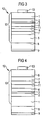
- the layer structure shown in FIG. 1 is the semiconductor body 12 of a SCH quantum well semiconductor laser.
- a semiconductor substrate 8 of a first conductivity type eg consisting of n-type GaAs
- a sequence of two oppositely conductive, highly doped, degenerate transition layers 6, 7 is applied, e.g. B. on the n-type semiconductor substrate 8, an n + -type transition layer 7 and thereon a p + -type transition layer 6.
- This sequence of transition layers 6, 7 serves as a buffer between a SCH quantum well structure arranged above the transition layers 6, 7 13. This is formed, for example, from cover layers, such as a first outer cladding layer 5 and a second outer cladding layer 1 and a first waveguide layer 4 and a second waveguide layer 2, and an active zone 3.
- the semiconductor substrate 8 and the transition layer 7 of a first line type e.g. hole or Electron line
- the transition layer 6 and the first Cladding layer 5 of an opposite to the first conductivity type second line type are the semiconductor substrate 8 and the transition layer 7 of a first line type (e.g. hole or Electron line) and the transition layer 6 and the first Cladding layer 5 of an opposite to the first conductivity type second line type.
- the conduction type of the second cladding layer 1 is also opposite to that of the first Sheath layer 5.
- the adaptation layer 11 can, however, also be omitted, so that the first outer cladding layer 5 is applied directly to the second transition layer 6.
- an ohmic rear contact 9 and an ohmic front contact 10 Form the electrical connection of the semiconductor body 12 an ohmic rear contact 9 and an ohmic front contact 10, wherein the ohmic back contact 9 on the Bottom side of the semiconductor substrate 8 and the ohmic front side contact 10 arranged on the second outer cladding layer 1 is.
- an n-type GaAs substrate 8 can Conventional n top contacts that can be produced in a simple manner be used.
- the second ohmic contact 10 can, for example, from a sequence of Ti / Pt / Au or from aluminum consist.
- the use of this highly doped n-type transition layer 7 advantageously prevents direct contact of BeTe with air, as a result of which technologically significant advantages are obtained and low-resistance contacts can be produced.
- the front side contact 10 can consist, for example, of a sequence of Ti / Pt / Au or aluminum.
- the refractive indices of the first degenerate transition layer 7, the second degenerate transition layer 6 and the adaptation layer 11 are advantageously the function as a waveguide customized. It is particularly important to ensure that the refractive indices of the outer cladding layers 1 and 5 smaller than in the other layers (second waveguide layer 2, active zone 3, first waveguide layer 4, second degenerate transition layer 6, first degenerate transition layer 7, adaptation layer 11).
- layers 1, 2, 5, 7, 8 are again the same Conduction type. In layers 4, 6, 11 this dominates opposite line type.
- the active zone 3 has a quantum well of z. B.
- the sum of the layer thicknesses of the layers 2, 3, 4, 6, 7, 11, that is to say the layers which act as waveguides, should advantageously not fall below 100 nm and not exceed 400 nm, whereas the cladding layers 1 and 5 are at least 200 nm thick should.
- high concentrations of Be and Mg in BeMgZnSe or Mg and S in ZnMgSSe can be achieved in the top layers 1 and 5, since experience has shown that the n-doping of these materials is more efficient than the p-doping. In this way, band gaps in the cover layers of more than 3.1 eV (300K) can be achieved. With these high concentrations, it is possible to improve the electrical charge carrier inclusion and to guide the optical wave better.
- Be x Mg y Zn 1-xy Te in components that emit short-wave light with wavelengths less than 460 nm. For this wavelength, Be x Mg y Zn 1-xy Te has a smaller refractive index than, for example, Be x Zn y Cd 1-x- y Se, whereby the optical wave using Be x Mg y Zn 1-xy Te in layer 6 and 11 is managed even better.
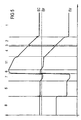
- the band diagram of the embodiment of the invention The component according to FIG. 3 is shown schematically in FIG. 5.
- the individual areas are analogous to the layer sequence designated by Figure 3.
- the charge carrier injection in this layered structure happens as follows: By applying an electrical voltage that is the pn junction whose p side from layers 6, 11 and 4 and its n-side layers 2 and 1, biased in the forward direction, electrons from contact 10 (not in Figure 5 drawn) over the cladding layer 1 and the waveguide layer 2 brought into active zone 3.
- the adjustment layer 11 prevented by an energy barrier, that negative charge carriers into the highly p-doped transition layer 6 can migrate (this function can alternatively layer 4).
- the SCH quantum well structure 13 are used in this example via the highly n-doped transition layer 7, the n-type outer cladding layer 5 and the n-GaAs substrate 8 electrons pulled out by applying the external voltage.
- the highly n-doped transition layer 7 and the highly p-doped transition layer 6 can electrons the valence band from the material of the p-doped transition layer 6 penetrate the barrier to the conduction band of transition layer 7, creating an effective hole current across the layers 6, 11 and 4 in the active zone 3 arises.
- the waveguide layer 2 and / or the outer cladding layer 1 an energy barrier for holes.
- n-doped (or n + -doped) and highly p-doped (or p + -doped), that is to say degenerate doping is advantageously to be understood as meaning a dopant concentration of von 10 17 cm -3 .
- Light-emitting diodes and laser diodes according to the invention can also be formed on the basis of other semiconductor materials, such as, for example, GaN or related mixed crystal systems, or II-IV semiconductors, such as CdTe, BeTe, BeSe, ZnS, MgS, CdSe, HgTe or related mixed crystal systems, such as Zn x Cd 1-x S y Se 1-y , Be x Zn y Cd 1-xy Te, Be x Mg y Zn 1-xy Te, Be x Mg y Zn 1-xy S or Be x Zn y Cd 1-xy S.
- GaP, ZnSe, Si, Ge, InP, InGaAs, ZnO, Al 2 O 3 , SiC or the like can be used.
Landscapes
- Physics & Mathematics (AREA)
- Optics & Photonics (AREA)
- Engineering & Computer Science (AREA)
- Condensed Matter Physics & Semiconductors (AREA)
- General Physics & Mathematics (AREA)
- Electromagnetism (AREA)
- Nanotechnology (AREA)
- Chemical & Material Sciences (AREA)
- Biophysics (AREA)
- Crystallography & Structural Chemistry (AREA)
- Life Sciences & Earth Sciences (AREA)
- Semiconductor Lasers (AREA)
- Led Devices (AREA)
Abstract
Description
Eine besonders bevorzugte Weiterbildung des erfindungsgemäßen optoelektronischen Bauelements ist ein SCH-Quantentopf-Laser, bei dem die aktive Zone, die Deckschichten (Wellenleiterschichten und äußere Mantelschichten) und die Übergangsschichten Halbleitermaterialien aus der Gruppe der berylliumhaltigen Chalkogenide aufweisen. Besonders bevorzugte Materialien sind beispielsweise für die aktive Zone BexZnyCd1-x-ySe (0 ≤ x ≤ 1, x+y ≤ 1), für die Deckschichten BexMgyZn1-x-ySe (0 ≤ x ≤ 1, 0 ≤ y ≤ 1, x+y ≤ 1) oder Zn1- xMgxSySe1-y (0 ≤ x ≤ 1, 0 ≤ y ≤ 1), für die p+-leitende Übergangsschicht hochdotiertes, p-leitendes BexMgyZn1-x-yTe (0 ≤ x ≤ 1, x+y ≤ 1) und für die n+-leitende Übergangsschicht hochdotiertes, n-leitendes InxGa1-xAs oder hochdotiertes, n-leitendes BexMgyZn1-x-ySe (0 ≤ x ≤ 1,
0 ≤ y ≤ 1, x+y ≤ 1). Zwischen der p+-leitenden Übergangsschicht und der dieser am nächsten liegenden Wellenleiterschicht ist vorzugsweise eine Anpassungsschicht angeordnet, die ein BeZnTeSe-Grading oder ein BeTe/ZnSe-Pseudograding aufweist. Bevorzugt ist bei dieser Weiterbildung ein bekanntermaßen auf einfache Weise in guter Qualität verfügbares n-leitendes GaAs-Halbleitersubstrat und ein besonders einfach herstellbarer herkömmlicher n-Vorderseitenkontakt verwendet.
BexZnyCd1-x-yTe, BexMgyZn1-x-yTe, BexMgyZn1-x-yS oder BexZnyCd1-x-yS. Als Subtrat können neben GaAs z. B. GaP, ZnSe, Si, Ge, InP, InGaAs, ZnO, Al2O3 ,SiC oder ähnliches verwendet sein.
Claims (13)
- Optoelektronisches Halbleiterbauelement mit einem zur Erzeugung einer elektromagnetischen Strahlung geeigneten Halbleiterkörper (12), bei dem über einem Halbleitersubstrat (8) eine aktive Zone (3) angeordnet ist, innerhalb der bei Stromfluss durch den Halbleiterkörper (12) die elektromagnetische Strahlung erzeugt wird und der mindestens eine p-dotierte ZnSe aufweisende II-VI-Halbleiterschicht zugeordnet ist, wobei als elektrische Ladungsträgerquelle zwischen der schlecht dotierbaren ZnSe aufweisenden. Halbleiterschnicht und einer dieser zugeordneten Kontaktschicht (9) des Halbleiterkörpers eine rückwärtsgepolte Schichtenfolge mit einer ersten hochdotierten entarteten Übergangsschicht (6) des ersten Leitungstyps und einer zweiten hochdotierten entarteten Übergangsschicht (7) eines dem ersten Leitungstyps entgegengesetzten zweiten Leitungstyps angeordnet ist, wobei sich die erste hochdotierte entartete Übergangsschicht (6) zwischen der schlecht dotierbaren Halbleiterschicht und der zweiten hochdotierten entarteten Übergangsschicht (7) befindet und die erste hochdotierte entartete Übergangsschicht (6) eine p+-leitende Übergangsschicht ist, dadurch gekennzeichnet, dass die erste hoch dotierte entartete Übergangsschicht (6) BeTe enthält.
- Optoelektronisches Halbleiterbauelement nach Anspruch 1,
dadurch gekennzeichnet, dass
die p-dotierte ZnSe aufweisende Schicht eine ZnMgSSe oder eine BeMgZnSe aufweisende II-VI-Halbleiterschicht enthält. - Optoelektronisches Halbleiterbauelement nach Anspruch 1 oder 2,
dadurch gekennzeichnet, dass
die p+-leitende Übergangsschicht BeMgZnTe oder BeZnCdTe aufweist. - Optoelektronisches Halbleiterbauelement nach einem der Ansprüche 1 bis 3,
dadurch gekennzeichnet, dass
die aktive Zone (3) eine zwischen einer ersten Wellenleiterschicht (4) und einer zweiten Wellenleiterschicht (2) angeordnete Quantentopfstruktur aufweist. - Optoelektronisches Halbleiterbauelement nach Anspruch 4,
dadurch gekennzeichnet, dass
die aktive Zone (3) und die erste und die zweite Wellenleiterschicht (2,4) zwischen einer ersten äußeren Mantelschicht (5) und einer zweiten äußeren Mantelschicht (1) angeordnet sind. - Optoelektronisches Halbleiterbauelement nach Anspruch 5,
dadurch gekennzeichnet, dass
die zweite äußere Mantelschicht (1) vom zweiten Leitungstyp ist und die erste äußere Mantelschicht (5) die schlecht dotierbare Halbleiterschicht aufweist und dass die erste hochdotierte entartete Übergangsschicht (6) und die zweite hochdotierte entartete Übergangsschicht (7) zwischen der zweiten äußeren Mantelschicht (5) und der dieser zugeordneten Kontaktschicht (9) des Halbleiterkörpers (12) angeordnet sind. - Optoelektronisches Halbleiterbauelement nach Anspruch 5,
dadurch gekennzeichnet, dass
die erste äußere Mantelschicht (5) und die zweite äußere Mantelschicht (1) vom zweiten Leitungstyp sind, und dass zwischen einer der beiden Wellenleiterschichten (2,4) und der dieser von der aktiven Zone (3) gesehen nachgeordneten äußeren Mantelschicht (1,5) die schlecht dotierbare Halbleiterschicht (11), die erste hochdotierte entartete Übergangsschicht (6) und die zweite hochdotierte entartete Übergargsschicht (7) angeordnet sind. - Optoelektronisches Halbleiterbauelement nach Anspruch 5,
dadurch gekennzeichnet, dass
die erste äußere Mantelschicht (5) und die zweite äußere Mantelschicht (1) vom zweiten Leitungstyp sind, dass auf einer der beiden Wellenleiterschichten (2,4) die erste hochdotierte entartete Übergangsschicht (6) und auf dieser die zweite hochdotierte entartete Übergangsschicht (7) aufgebracht ist und dass dieser eine der äußeren Mantelschichten (1,5) von der aktiven Zone (3) aus gesehen nachgeordnet ist. - Optoelektronisches Halbleiterbauelement nach einem der Ansprüche 1 bis 8,
dadurch gekennzeichnet, dass
die aktive Zone (3) Halbleitermaterial aus der Gruppe der berylliumhaltigen Chalkogenide oder Zn1-xCdxSySe1-y aufweist. - Optoelektronisches Halbleiterbauelement nach einem der Ansprüche 4 bis 8 oder nach einem der Ansprüche 4 bis 8 und Anspruch 9,
dadurch gekennzeichnet, dass
die erste Wellenleiterschicht (4) und die zweite Wellenleiterschicht (2) Halbleitermaterial aus der Gruppe der berylliumhaltigen Chalkogenide aufweisen. - Optoelektronisches Halbleiterbauelement nach einem der Ansprüche 5 bis 8 oder nach einem der Ansprüche 5 bis 8 und Anspruch 9 oder 10,
dadurch gekennzeichnet, dass
die erste äußere Mantelschicht (5) und die zweite äußere Mantelschicht (1) Halbleitermaterial aus der Gruppe der berylliumhaltigen Chalkogenide aufweisen. - Optoelektronisches Halbleiterbauelement nach einem der Ansprüche 1 bis 11,
dadurch gekennzeichnet, dass
die p+-leitende Übergangsschicht (6) mit einem Dotierstoff aus der Gruppe As, Sb, P, K, Rb, Cs, C, Si, Ge und Sn dotiert ist. - Optoelektronisches Halbleiterbauelement nach einem der Ansprüche 5 bis 8 oder nach einem der Ansprüche 5 bis 8 und einem der Ansprüche 9 bis 12,
dadurch gekennzeichnet, dass
der Abstand zwischen den beiden Mantelschichten (1,4) zwischen etwa 100 nm und etwa 400 nm beträgt und dass die erste Mantelschicht (5) und die zweite Mantelschicht (1) jeweils eine Dicke von mindestens 200 nm aufweisen.
Applications Claiming Priority (3)
| Application Number | Priority Date | Filing Date | Title |
|---|---|---|---|
| DE19703615A DE19703615A1 (de) | 1997-01-31 | 1997-01-31 | Optoelektronisches Halbleiterbauelement |
| DE19703615 | 1997-01-31 | ||
| PCT/DE1998/000263 WO1998034284A1 (de) | 1997-01-31 | 1998-01-29 | Optoelektronisches halbleiterbauelement |
Publications (2)
| Publication Number | Publication Date |
|---|---|
| EP0956601A1 EP0956601A1 (de) | 1999-11-17 |
| EP0956601B1 true EP0956601B1 (de) | 2003-03-19 |
Family
ID=7818930
Family Applications (1)
| Application Number | Title | Priority Date | Filing Date |
|---|---|---|---|
| EP98907874A Expired - Lifetime EP0956601B1 (de) | 1997-01-31 | 1998-01-29 | Optoelektronisches halbleiterbauelement |
Country Status (7)
| Country | Link |
|---|---|
| US (1) | US6147365A (de) |
| EP (1) | EP0956601B1 (de) |
| JP (1) | JP3486193B2 (de) |
| KR (1) | KR20000070646A (de) |
| CN (1) | CN1252169A (de) |
| DE (2) | DE19703615A1 (de) |
| WO (1) | WO1998034284A1 (de) |
Families Citing this family (10)
| Publication number | Priority date | Publication date | Assignee | Title |
|---|---|---|---|---|
| JP3404064B2 (ja) * | 1993-03-09 | 2003-05-06 | 株式会社日立製作所 | 半導体装置及びその製造方法 |
| JP3464629B2 (ja) * | 1999-06-25 | 2003-11-10 | 日本碍子株式会社 | p型コンタクト電極装置および発光装置 |
| US6797412B1 (en) * | 2000-04-11 | 2004-09-28 | University Of Connecticut | Full color display structures using pseudomorphic cladded quantum dot nanophosphor thin films |
| NO20041523L (no) * | 2003-09-19 | 2005-03-21 | Sumitomo Electric Industries | Lysemitterende halvlederelement |
| US7745814B2 (en) * | 2004-12-09 | 2010-06-29 | 3M Innovative Properties Company | Polychromatic LED's and related semiconductor devices |
| US7719015B2 (en) * | 2004-12-09 | 2010-05-18 | 3M Innovative Properties Company | Type II broadband or polychromatic LED's |
| US7402831B2 (en) * | 2004-12-09 | 2008-07-22 | 3M Innovative Properties Company | Adapting short-wavelength LED's for polychromatic, broadband, or “white” emission |
| JP4920344B2 (ja) * | 2006-08-25 | 2012-04-18 | 株式会社日立製作所 | 半導体レーザ |
| EP2171760A1 (de) * | 2007-06-28 | 2010-04-07 | Solar Systems & Equipments S.R.L. | Verfahren zur bildung eines nichtgleichrichtenden rückkontakts in einer cdte/cds-dünnfilm-solarzelle |
| US10454250B2 (en) * | 2017-05-22 | 2019-10-22 | Lasertel Inc. | Thermal contact for semiconductors and related methods |
Family Cites Families (9)
| Publication number | Priority date | Publication date | Assignee | Title |
|---|---|---|---|---|
| US5010374A (en) * | 1990-06-05 | 1991-04-23 | At&T Bell Laboratories | Quantum well laser utilizing an inversion layer |
| US5248631A (en) * | 1990-08-24 | 1993-09-28 | Minnesota Mining And Manufacturing Company | Doping of iib-via semiconductors during molecular beam epitaxy using neutral free radicals |
| US5268918A (en) * | 1991-02-21 | 1993-12-07 | Sony Corporation | Semiconductor laser |
| KR950007490B1 (ko) * | 1991-12-28 | 1995-07-11 | 엘지전자주식회사 | 반도체 레이저 |
| US5363395A (en) * | 1992-12-28 | 1994-11-08 | North American Philips Corporation | Blue-green injection laser structure utilizing II-VI compounds |
| JPH077218A (ja) * | 1993-06-15 | 1995-01-10 | Sony Corp | 半導体レーザ |
| JP3239550B2 (ja) * | 1993-08-30 | 2001-12-17 | ソニー株式会社 | 半導体レーザ |
| US5338944A (en) | 1993-09-22 | 1994-08-16 | Cree Research, Inc. | Blue light-emitting diode with degenerate junction structure |
| US5892784A (en) * | 1994-10-27 | 1999-04-06 | Hewlett-Packard Company | N-drive p-common surface emitting laser fabricated on n+ substrate |
-
1997
- 1997-01-31 DE DE19703615A patent/DE19703615A1/de active Pending
-
1998
- 1998-01-29 EP EP98907874A patent/EP0956601B1/de not_active Expired - Lifetime
- 1998-01-29 JP JP53244798A patent/JP3486193B2/ja not_active Expired - Fee Related
- 1998-01-29 DE DE59807557T patent/DE59807557D1/de not_active Expired - Lifetime
- 1998-01-29 KR KR1019997006895A patent/KR20000070646A/ko not_active Abandoned
- 1998-01-29 CN CN98803918A patent/CN1252169A/zh active Pending
- 1998-01-29 WO PCT/DE1998/000263 patent/WO1998034284A1/de not_active Ceased
-
1999
- 1999-08-02 US US09/364,898 patent/US6147365A/en not_active Expired - Lifetime
Also Published As
| Publication number | Publication date |
|---|---|
| JP2001511310A (ja) | 2001-08-07 |
| US6147365A (en) | 2000-11-14 |
| JP3486193B2 (ja) | 2004-01-13 |
| CN1252169A (zh) | 2000-05-03 |
| KR20000070646A (ko) | 2000-11-25 |
| EP0956601A1 (de) | 1999-11-17 |
| WO1998034284A1 (de) | 1998-08-06 |
| DE59807557D1 (de) | 2003-04-24 |
| DE19703615A1 (de) | 1998-08-06 |
Similar Documents
| Publication | Publication Date | Title |
|---|---|---|
| EP0986846B1 (de) | Optoelektronisches halbleiterbauelement | |
| EP0996985B1 (de) | II-VI-HALBLEITERBAUELEMENT MIT MINDESTENS EINEM ÜBERGANG VON EINER Se-ENTHALTENDEN SCHICHT AUF EINE BeTe-ENTHALTENDE SCHICHT UND VERFAHREN ZUM HERSTELLEN DES ÜBERGANGES | |
| DE69510129T2 (de) | Oberflächenemittierende lumineszente Halbleitervorrichtung | |
| DE102007057674A1 (de) | LED mit Stromaufweitungsschicht | |
| US5373521A (en) | Blue light emitting semiconductor device and method of fabricating the same | |
| DE19957312A1 (de) | Licht emittierende Diode | |
| WO2009039830A1 (de) | Optoelektronischer halbleiterchip mit einer mehrfachquantentopfstruktur | |
| DE19542241C2 (de) | Optoelektronisches Bauelement in II-VI-Halbleitermaterial | |
| WO2008014772A1 (de) | Led-halbleiterkörper | |
| DE19935998B4 (de) | Mehrfach-Halbleiterlaserstruktur mit schmaler Wellenlängenverteilung | |
| DE102006051745A1 (de) | LED-Halbleiterkörper und Verwendung eines LED-Halbleiterkörpers | |
| EP0956601B1 (de) | Optoelektronisches halbleiterbauelement | |
| WO2009036730A2 (de) | Optoelektronischer halbleiterchip mit quantentopfstruktur | |
| WO2018138081A1 (de) | Optoelektronischer halbleiterchip | |
| KR100292308B1 (ko) | 반도체장치 | |
| DE69405486T2 (de) | Halbleitervorrichtung mit Gradienten-Bandabstand BeTe-ZnSe ohmschem Kontakt für einen II-VI Halbleiter | |
| DE102017122032A1 (de) | Laserdiode | |
| US7065124B2 (en) | Electron affinity engineered VCSELs | |
| WO2023213480A1 (de) | Optoelektronisches halbleiterbauelement und verfahren zur herstellung eines optoelektronischen halbleiterbauelements | |
| EP0956626B1 (de) | Kantenemittierendes halbleiterlaser-bauelement | |
| DE69505341T2 (de) | HALBLEITER-HETEROSTRUKTUR, DIE EINE II-VI-VERBINDUNG ENTHÄLT, IN OHMSCHEM KONTAKT MIT EINEM p-GaAs SUBSTRAT | |
| DE3202832A1 (de) | Hochempfindlicher fotodetektor | |
| WO2023104668A1 (de) | Vcsel, sender zum senden optischer signalpulse mit einem vcsel, verfahren zum betreiben eines vcsel sowie verfahren zum herstellen eines vcsel | |
| WO2016174240A1 (de) | Kantenemittierender halbleiterlaser mit tunnelkontakt | |
| DE102007035896A1 (de) | Optoelektronischer Halbleiterkörper und optoelektronisches Bauelement |
Legal Events
| Date | Code | Title | Description |
|---|---|---|---|
| PUAI | Public reference made under article 153(3) epc to a published international application that has entered the european phase |
Free format text: ORIGINAL CODE: 0009012 |
|
| 17P | Request for examination filed |
Effective date: 19990720 |
|
| AK | Designated contracting states |
Kind code of ref document: A1 Designated state(s): DE FR GB IT |
|
| RAP1 | Party data changed (applicant data changed or rights of an application transferred) |
Owner name: INFINEON TECHNOLOGIES AG |
|
| GRAG | Despatch of communication of intention to grant |
Free format text: ORIGINAL CODE: EPIDOS AGRA |
|
| RIC1 | Information provided on ipc code assigned before grant |
Free format text: 7H 01L 33/00 A, 7H 01S 5/32 B |
|
| 17Q | First examination report despatched |
Effective date: 20020405 |
|
| GRAG | Despatch of communication of intention to grant |
Free format text: ORIGINAL CODE: EPIDOS AGRA |
|
| GRAH | Despatch of communication of intention to grant a patent |
Free format text: ORIGINAL CODE: EPIDOS IGRA |
|
| GRAH | Despatch of communication of intention to grant a patent |
Free format text: ORIGINAL CODE: EPIDOS IGRA |
|
| GRAA | (expected) grant |
Free format text: ORIGINAL CODE: 0009210 |
|
| AK | Designated contracting states |
Designated state(s): DE FR GB IT |
|
| PG25 | Lapsed in a contracting state [announced via postgrant information from national office to epo] |
Ref country code: IT Free format text: LAPSE BECAUSE OF FAILURE TO SUBMIT A TRANSLATION OF THE DESCRIPTION OR TO PAY THE FEE WITHIN THE PRESCRIBED TIME-LIMIT;WARNING: LAPSES OF ITALIAN PATENTS WITH EFFECTIVE DATE BEFORE 2007 MAY HAVE OCCURRED AT ANY TIME BEFORE 2007. THE CORRECT EFFECTIVE DATE MAY BE DIFFERENT FROM THE ONE RECORDED. Effective date: 20030319 |
|
| REG | Reference to a national code |
Ref country code: GB Ref legal event code: FG4D Free format text: NOT ENGLISH |
|
| REF | Corresponds to: |
Ref document number: 59807557 Country of ref document: DE Date of ref document: 20030424 Kind code of ref document: P |
|
| GBT | Gb: translation of ep patent filed (gb section 77(6)(a)/1977) |
Effective date: 20030723 |
|
| ET | Fr: translation filed | ||
| PLBE | No opposition filed within time limit |
Free format text: ORIGINAL CODE: 0009261 |
|
| STAA | Information on the status of an ep patent application or granted ep patent |
Free format text: STATUS: NO OPPOSITION FILED WITHIN TIME LIMIT |
|
| 26N | No opposition filed |
Effective date: 20031222 |
|
| REG | Reference to a national code |
Ref country code: DE Ref legal event code: R082 Ref document number: 59807557 Country of ref document: DE Representative=s name: EPPING HERMANN FISCHER, PATENTANWALTSGESELLSCH, DE |
|
| REG | Reference to a national code |
Ref country code: DE Ref legal event code: R082 Ref document number: 59807557 Country of ref document: DE Representative=s name: EPPING HERMANN FISCHER, PATENTANWALTSGESELLSCH, DE Effective date: 20120730 Ref country code: DE Ref legal event code: R081 Ref document number: 59807557 Country of ref document: DE Owner name: OSRAM OPTO SEMICONDUCTORS GMBH, DE Free format text: FORMER OWNER: INFINEON TECHNOLOGIES AG, 81669 MUENCHEN, DE Effective date: 20120730 |
|
| REG | Reference to a national code |
Ref country code: FR Ref legal event code: TP Owner name: OSRAM OPTO SEMICONDUCTORS GMBH, DE Effective date: 20120820 |
|
| REG | Reference to a national code |
Ref country code: GB Ref legal event code: 732E Free format text: REGISTERED BETWEEN 20120920 AND 20120926 |
|
| REG | Reference to a national code |
Ref country code: FR Ref legal event code: PLFP Year of fee payment: 18 |
|
| PGFP | Annual fee paid to national office [announced via postgrant information from national office to epo] |
Ref country code: DE Payment date: 20150121 Year of fee payment: 18 |
|
| PGFP | Annual fee paid to national office [announced via postgrant information from national office to epo] |
Ref country code: GB Payment date: 20150121 Year of fee payment: 18 Ref country code: FR Payment date: 20150122 Year of fee payment: 18 |
|
| REG | Reference to a national code |
Ref country code: DE Ref legal event code: R119 Ref document number: 59807557 Country of ref document: DE |
|
| GBPC | Gb: european patent ceased through non-payment of renewal fee |
Effective date: 20160129 |
|
| REG | Reference to a national code |
Ref country code: FR Ref legal event code: ST Effective date: 20160930 |
|
| PG25 | Lapsed in a contracting state [announced via postgrant information from national office to epo] |
Ref country code: DE Free format text: LAPSE BECAUSE OF NON-PAYMENT OF DUE FEES Effective date: 20160802 Ref country code: GB Free format text: LAPSE BECAUSE OF NON-PAYMENT OF DUE FEES Effective date: 20160129 |
|
| PG25 | Lapsed in a contracting state [announced via postgrant information from national office to epo] |
Ref country code: FR Free format text: LAPSE BECAUSE OF NON-PAYMENT OF DUE FEES Effective date: 20160201 |