EP0957502B1 - Herstellungsverfahren einer Plasmaentladungs-Anzeigeplatte - Google Patents
Herstellungsverfahren einer Plasmaentladungs-Anzeigeplatte Download PDFInfo
- Publication number
- EP0957502B1 EP0957502B1 EP99303665A EP99303665A EP0957502B1 EP 0957502 B1 EP0957502 B1 EP 0957502B1 EP 99303665 A EP99303665 A EP 99303665A EP 99303665 A EP99303665 A EP 99303665A EP 0957502 B1 EP0957502 B1 EP 0957502B1
- Authority
- EP
- European Patent Office
- Prior art keywords
- glass
- particle diameter
- dielectric
- average particle
- layer
- Prior art date
- Legal status (The legal status is an assumption and is not a legal conclusion. Google has not performed a legal analysis and makes no representation as to the accuracy of the status listed.)
- Expired - Lifetime
Links
Images



Classifications
-
- H—ELECTRICITY
- H01—ELECTRIC ELEMENTS
- H01J—ELECTRIC DISCHARGE TUBES OR DISCHARGE LAMPS
- H01J9/00—Apparatus or processes specially adapted for the manufacture, installation, removal, maintenance of electric discharge tubes, discharge lamps, or parts thereof; Recovery of material from discharge tubes or lamps
- H01J9/24—Manufacture or joining of vessels, leading-in conductors or bases
-
- H—ELECTRICITY
- H01—ELECTRIC ELEMENTS
- H01J—ELECTRIC DISCHARGE TUBES OR DISCHARGE LAMPS
- H01J11/00—Gas-filled discharge tubes with alternating current induction of the discharge, e.g. alternating current plasma display panels [AC-PDP]; Gas-filled discharge tubes without any main electrode inside the vessel; Gas-filled discharge tubes with at least one main electrode outside the vessel
- H01J11/10—AC-PDPs with at least one main electrode being out of contact with the plasma
- H01J11/12—AC-PDPs with at least one main electrode being out of contact with the plasma with main electrodes provided on both sides of the discharge space
-
- H—ELECTRICITY
- H01—ELECTRIC ELEMENTS
- H01J—ELECTRIC DISCHARGE TUBES OR DISCHARGE LAMPS
- H01J11/00—Gas-filled discharge tubes with alternating current induction of the discharge, e.g. alternating current plasma display panels [AC-PDP]; Gas-filled discharge tubes without any main electrode inside the vessel; Gas-filled discharge tubes with at least one main electrode outside the vessel
- H01J11/20—Constructional details
- H01J11/34—Vessels, containers or parts thereof, e.g. substrates
- H01J11/38—Dielectric or insulating layers
-
- H—ELECTRICITY
- H01—ELECTRIC ELEMENTS
- H01J—ELECTRIC DISCHARGE TUBES OR DISCHARGE LAMPS
- H01J9/00—Apparatus or processes specially adapted for the manufacture, installation, removal, maintenance of electric discharge tubes, discharge lamps, or parts thereof; Recovery of material from discharge tubes or lamps
- H01J9/02—Manufacture of electrodes or electrode systems
Definitions
- the present invention relates to a plasma display panel used for a display device, and especially relates to a plasma display panel including an improved dielectric glass layer.
- a CRT display is superior to a plasma display panel and a liquid crystal display in resolution and image quality.
- a CRT display is not suitable for a large screen that measures more than 1.016 m (40 inches) because the depth dimension and the weight are too large.
- a liquid crystal display is superior in consuming a relatively low power and requiring a relatively low voltage.
- a liquid crystal display has disadvantages of a limited screen size and viewing angle.
- a plasma display panel realizes a large screen. Screens that measure in the 1.016 m (40 inches) have been developed using plasma display panels (described in " Kino Zairyo (Functional Materials)" (Vol. 16, No. 2, February issue, 1996, p7), for instance).
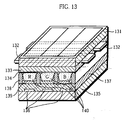
- Fig. 13 is a perspective view of the essential part of a conventional ac plasma display panel.
- a reference number 131 refers to a front glass substrate made of borosilicate sodium glass.
- display electrodes 132 are formed on the surface of the front glass substrate.
- the display electrodes 132 are covered by a dielectric glass layer 133.
- the surface of the dielectric glass layer 133 is covered by a magnesium oxide (MgO) dielectric protective layer 134.
- the dielectric glass layer is formed using a glass powder the particle diameter of which ranges from 2 to 15 ⁇ m on average.
- a reference number 135 refers to a back glass substrate. On the surface of the back glass substrate 135, address electrodes 136 are formed. The address electrodes 135 are covered by a dielectric glass layer 137. On the surface of the dielectric glass layer 137, walls 138 and phosphor layers 139 are formed. Between the walls 138, discharge spaces 140 are formed. The discharge spaces 140 are filled with discharge gas.
- a full-specification, high-definition TV is expected to realize the pixel level given below.
- the number of pixels is 1920 X 1125.
- the dot pitch is 0.15mm X 0.48mm for a screen that measures around 1.0668 m (42 inches).
- the area of one cell is as small as 0.072mm 2 .
- the area is 1/7 to 1/8 compared with a 1.0668 m (42-inch), high-definition TV according to a conventional NTSC (National Television System Committee) (the number of pixels is 640 X 480, the dot pitch is 0.43mm X 1.29mm, and the area of one cell is 0.55mm 2 ).
- NTSC National Television System Committee
- the discharge space is smaller for the full-specification, high-definition TV.
- the plasma display panel gains the same capacity as a capacitor, it is necessary to set the thickness of the dielectric glass layers 133 and 137 to be smaller than in a conventional one.
- a glass paste is made of a glass powder the particle diameter and the softening point of which ranges from 2 to 15 ⁇ m on average and from 550 to 600°C, and a solvent such as terpineol including ethyl cellulose and butyl carbitol acetate using a trifurcated roll.
- the glass paste is printed on the front glass substrate according to a screen printing method (the glass paste is adjusted so that the viscosity is 50 to 100 Pa.s (50,000 to 100,000cp), which is suitable for the screen printing method).
- the printed glass paste is dried, and undergoes sintering at a temperature around the softening point of the glass powder (550 to 600°C), forming a dielectric glass layer.
- the melted glass rarely reacts to the electrode made of Ag, ITO, Cr-Cu-Cr, or the like since the glass paste undergoes sintering at a temperature around the glass powder softening point and the glass is inert, i.e., the glass does not flow well.
- the resistance of the electrode does not increase, the electrode ingredients do not dispersed in or not color the glass, and a dielectric glass layer is formed with one firing.
- the glass paste does not flow well since the particle diameter of the glass powder ranges from 2 to 15 ⁇ m on average and the glass paste is fired at a temperature around the softening point of the glass powder, and the mesh pattern of the screen remains in this method.
- the surface of the formed dielectric glass layer is rough (the surface roughness is 4 to 6 ⁇ m), and visible light is scattered on the coarse surface.
- the dielectric glass layer is a ground glass and the transmittance is relatively low.
- bubbles and pinholes appear in the formed dielectric glass layer, so that the voltage endurance of the dielectric glass layer is decreased.
- the voltage endurance means the limitation of the insulation effect of a dielectric glass layer when a voltage is applied to the dielectric glass layer.
- a glass paste (the viscosity is 35 to 50 Pa.s (35,000 to 50,000cp (centipoise))) is made using a low-melting lead glass powder (the proportion of PbO is about 75%) the particle diameter and the softening point of which ranges from 2 to 15 ⁇ m on average and from 450 to 500°C.
- the glass paste is printed on the front glass substrate according to a screen printing method and dried.
- the dried glass paste undergoes sintering at a temperature about 100°C higher than the softening point of the glass powder, i.e., at 550 to 600°C, forming a dielectric glass layer.
- the surface of the formed dielectric glass layer is smooth (surface roughness is about 2 ⁇ m) since the sintering temperature is considerably higher than the softening point and the glass paste flows well.
- a dielectric glass layer is formed with one sintering.
- the melted glass reacts to the electrode made of Ag, ITO, Cr-Cu-Cr, or the like since the glass paste is activated and flows well. As a result, the resistance of the electrode increases and the dielectric glass layer is colored. In addition, large bubbles are likely to appear in the dielectric glass layer as a result of the reaction to the electrode.
- the third method is the combination of the first and second methods (refers to Japanese Laid-Open Patent Application Nos. 7-105855 and 9-50769).
- a glass paste is made of a glass powder the particle diameter and the softening point of which ranges from 2 to 15 ⁇ m on average and from 550 to 600°C.
- the glass paste is printed on the front glass substrate according to the screen printing method.
- the printed glass paste is dried, and undergoes sintering at a temperature around the softening point, forming a dielectric glass layer. On the formed dielectric glass layer, another dielectric glass layer is further formed.
- a glass paste is made of a glass powder the particle diameter and the softening point of which ranges from 2 to 15 ⁇ m on average and from 450 to 50.0°C.
- the second glass paste is printed on the previously formed dielectric glass layer according to the screen printing method.
- the printed second glass paste is dried, and undergoes sintering at a temperature about 100°C higher than softening point, i.e., at 550 to 600°C, forming the second dielectric glass layer.
- the melted glass rarely reacts to the electrode and the surface of the dielectric glass layer is smooth, resulting in an improved transmittance of visible light and endurance to voltage.
- the method of forming the dielectric galls layer is complicated and thinner dielectric glass layer, which is necessary to improve the intensity, is difficult to form.
- the visible light transmittance is not improved so much since bubbles appear in the first formed dielectric glass layer.
- JP 11060274A relates to obtaining a dielectric layer by specifying a particle diameter of glass powder contained in a dielectric-forming material of a PDP.
- the glass powder has a 50% particle diameter of between 0.5 micron and 2 micron, and a preferable maximum particle diameter of between 5 micron and 15 micron.
- the above-mentioned object may be achieved by the manusfacturing method of plasma display given below.
- the present invention provides a manufacturing method of a plasma display panel, the plasma display panel comprising a front panel, including a front glass substrate on which a first electrode and a first dielectric glass layer have been formed, and a back panel, including a back glass substrate on which a second electrode and a phosphor layer have been formed, the front and back panels being positioned so that the first and second electrodes face each other at a predetermined distance, walls being formed between the front and back panels, and spaces surrounded by the front panels, the back panel, and the walls being filled with a dischargeable gas, wherein the first dielectric glass layer is formed by applying a first glass paste on the front glass substrate, the first glass paste being a mixture of the first glass powder, at least one of the plasticizer and a surface active agent, a binder, and a binder dissolution solvent, characterised in that the first glass powder has an average particle diameter of 0.1 to 1.5 ⁇ m and a maximum particle diameter that is no greater than three times the average particle diameter.
- the object of the present invention may be realised since a dielectric glass layer having a relatively smooth surface and including a minimum amount of bubbles is formed using the glass powder that has been described.
- the back panel further includes a second dielectric glass layer
- the plasma display panel manufacturing method forms the second dielectric glass layer by applying a second glass paste on the back glass substrate, the second glass paste being a mixture of the second glass powder, at least one of a plasticizer and a surface active agent, a binder, and a binder dissolution solvent, the second glass powder with an average particle diameter of 0.1 to 1.5 ⁇ m and a maximum particle diameter that is no greater than three times the average particle diameter.
- the first glass plate may include a titanium oxide with an average particle diameter of 0.1 to 0.5 ⁇ m.
- the second glass paste may include a titanium oxide powder with an average particle diameter of 0.1 to 0.5 ⁇ m.
- Fig. 1 is a perspective view of the essential part of an ac discharge PDP according to the present embodiment.
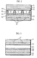
- Fig. 2 is a vertical sectional view taken on line X-X of Fig. 1.
- Fig. 3 is a vertical sectional view taken on line Y-Y of Fig. 1.
- the number of cells is three in Figs. 1 to 3 for convenience in explanation, a large number of cells each of which emits light of red (R), green (G), or blue (B) are arranged on the PDP.
- FIGs. 1 to 3 shows the structure of the PDP.
- a front panel 10 is stuck to a back panel 20.
- the front panel 10 is formed by placing discharge electrodes (display electrodes) 12, a dielectric glass layer 13, and a protective layer 14 on a front glass substrate 11.
- the back panel 20 is formed by placing address electrodes 22, a dielectric glass layer 23, walls 24, and phosphor layers 25, each of which has a different color "R (red)", “C (green)", and “B (blue)", on a back glass substrate 21.
- discharge gas is filled in discharge spaces 30 between the front panel 10 and the back panel 20, discharge gas is filled.
- a metal electrode made of Ag, or Cr-Cu-Cr is placed as a bus line on a transparent electrode made of ITO or SnO 2 (not illustrated).
- V dQ / ⁇ ⁇ S
- the discharge spaces are in plasma condition at the time of discharge, so that the discharge spaces are conductive elements.
- the capacitance "C” as a capacitor is increased and the discharge voltage at the time of addressing and display is decreased.
- the approach to the improvement of the voltage endurance and the visible light transmittance is the determination of the average and maximum particle diameter of the glass powder in the dielectric glass layers 13 and 23.
- the discharge electrodes are formed in parallel according to the photolithographic method, which is well known in the art. Then, the dielectric glass layer is formed using a glass material to cover the discharge electrodes 12, which will be explained later in detail.
- the protective layer 14 made of magnesium oxide (MgO) is formed on the surface of the dielectric glass layer 13.
- Figs. 4A to 4E show the process of forming the discharge electrode 12 according to the photolithographic method.
- a predetermined thickness (for instance, 0.12 ⁇ m) of ITO layer 41 is formed by sputtering on the front glass substrate 11 as shown in Fig. 4A.
- a photoregister layer 42 is formed as shown in Fig. 4B.
- light beams 44 are applied using masks 43, and a predetermined width (for instance, 150 ⁇ m) of ITO electrodes 45 are formed in parallel after development (the interval between the ITO electrodes 45 is, for instance, 50 ⁇ m) as shown in Fig. 4D.
- a light-sensitive silver paste is applied across the surface as shown in Fig.
- the metal electrodes are formed in the manner given below. Each of the metal layers is vaporized in the sputtering on the transparent electrodes that have been formed by patterning as has been described. Resists are applied on the surface of the vaporized layers, and metal electrodes are formed by patterning according to the photolithographic method.
- Fig. 5 is a schematic diagram of a CVD device 50 used in forming a protective layer 14.
- the CVD device 50 performs a heat CVD and a plasma CVD.
- a heater 56 for heating a glass substrate 57 (the front glass substrate 11 on which the discharge electrode and the dielectric glass layer 13 are formed in Fig. 1) is included.
- the pressure in the CVD device body 55 is reduced by an exhaust device 59.
- a high-frequency power supply 58 for generating plasma in the CVD device body 55 is included in the CVD device 50.
- Ar gas cylinders. 51a and 51b provide the CVD device body 55 with argon [Ar] gas that is a carrier via vaporizers (bubblers) 52 and 53.
- a magnesium compound is stored for forming the protective layer 14. More specifically, a metal chelate such as acetylacetone magnesium [Mg(C 5 H 7 O 2 ) 2 ], a cyclopentadienyl compound such as cyclopentadienyl magnesium [Mg(C 5 H 5 ) 2 ], and an alkoxide compound is stored in the vaporizers 52 and 53.
- a metal chelate such as acetylacetone magnesium [Mg(C 5 H 7 O 2 ) 2 ]
- a cyclopentadienyl compound such as cyclopentadienyl magnesium [Mg(C 5 H 5 ) 2 ]
- an alkoxide compound is stored in the vaporizers 52 and 53.
- An oxygen cylinder 54 provides the CVD device body 55 with oxygen [O 2 ] that is a reactant gas.
- the glass substrate 57 is placed on the heater 56 with the side on which the electrodes have been formed up, and is heated at a predetermined temperature (about 30 0°C). Meanwhile, the pressure in the CVD device body 55 is reduced (to about a several tens of Torr) by the exhaust device 59.
- Ar gas is put from the Ar gas cylinder 51a and 51b while a source is heated to a predetermined vaporization temperature. Meanwhile, oxygen is provided by the oxygen cylinder 54 into the CVD device body 55.
- the metal chelate, the cyclopentadienyl compound, or the alkoxide compound put into the CVD device body 55 is reacted to the oxygen that is also put into the CVD device body 55.
- the protective layer 14 is formed on the surface of the glass substrate 57, on which electrodes have been formed.
- the protective layer 14 is formed in almost the same procedure using the CVD device.
- the plasma CVD differs from the heat CVD 58 in the points that the high-frequency power is driven and a high-frequency electric field (13.56MHz) is applied.
- the protective layer 14 is formed while plasma is caused in the CVD device body 55.
- the back panel 20 is formed in the manner given below.
- the address electrodes 22 are formed on the surface of the back glass substrate 21 according to the photolithographic method. Note that the address electrodes 22 are made of metal electrodes.
- the dielectric glass layer 23 is formed in the same manner as the front panel 10 so that the dielectric glass layer 23 covers the address electrodes 22.
- the forming of the dielectric glass layer 23 will be explained later in detail.
- walls 24 made of glass are placed at a predetermine interval.
- phosphors of a red (“R”) phosphor, a green (“G”) phosphor, and a blue (“B”) phosphor are arranged to form phosphor layers 25.
- R red
- G green
- B blue
- the phosphor that is generally used for a PDP may be used, another kind of phosphor is used for the "R”, "G", and "B” phosphors.
- Fig. 6 is a schematic diagram of an ink coating device 60 used in forming a phosphor layer.
- a phosphor mixture of a red phosphor Y 2 O 3 :Eu 3+ powder, ethyl cellulose, and a solvent ( ⁇ -terpineol) (the mixture ratio is 50wt%:1.0wt%:49wt%) having a predetermined particle diameter (for instance, the average particle diameter is 2.0 ⁇ m) is stirred using a sand mill in the server 61.
- red-phosphor-forming liquid 64 is injected from the nozzle unit 63 (the diameter is 60 ⁇ m) of an injector at the pressure of a pump 62 into an interval between walls 24, which has forms of stripes.
- the substrate is moved straightly to form a red phosphor line 25.
- a blue phosphor line (BaMgAl 10 O 17 :Eu 2+ ) and a green phosphor line (Zn 2 SiO 4 :Mn) are formed.
- the red, blue, and green phosphor lines are fired at a predetermined temperature (for instance, at 500 °C) for a predetermined period of time (for instance, for 10 minutes) to form the phosphor layers 25.
- the front panel 10 is stuck to the back panel 20 using an attaching glass, the inside of the discharge spaces 30 divided by the walls 24 are exhausted to a high degree of vacuum 1.067 x 10 -4 Pa (8 x 10 -7 Torr)). After that a predetermined composition of discharge gas is filled at a predetermined pressure to form a PDP.
- the cell size of the PDP in the present embodiment is set so that the cell size is suitable for a high-definition TV whose screen measures in the 1.016 m (40 inches). More specifically, the interval of the walls 24 is set to be equal to or smaller than 0.2mm and the distance between the discharge electrodes 12 is set to be equal to or smaller than 0.1mm.
- the discharge gas filled into the discharge spaces 30 is a He-Xe or a Ne-Xe gas that has been used.
- the composition is set so that the content of Xe is equal to or more than 5vol% and the infusion pressure is 6.666 x 10 4 to 9.999 x 10 4 (500 to 760Torr).
- the dielectric glass layer 13 is formed on the surface of the front glass substrate 11 on which the discharge electrodes 12 have been formed according to the screen printing method, the die coating method, the spin coating method, the spray coating method, or the blade coating method using a glass powder the average particle diameter of which is 0.1 to 1.5 ⁇ m and the maximum particle diameter of which is equal to or smaller than three times the average particle diameter.
- a dielectric glass layer that is a solid sintered metal oxide that include a relatively small number of bubbles and has a relatively smooth surface may be obtained.
- the particle diameters are measured using a Coulter counter grading analyzer (a particle size measuring instrument of Coulter K.K.), by which the number of particles are counted for each particle diameter (the Coulter Counter is also used in the examples given below).
- the particle diameters are adjusted by crushing the glass raw material so that a predetermined particle diameter would be obtained using a crusher such as a ball mill and a jet mill (for instance, HJP300-02 of Sugino Machine Limited).
- a crusher such as a ball mill and a jet mill (for instance, HJP300-02 of Sugino Machine Limited).
- the components G1, G2, G3, ..., GN are weighed according to the component ratio, melted in a furnace at 1300°C, and put into water.
- the glass material is a PbO-B 2 O 3 -SiO 2 -CaO glass, a PbO-B 2 O 3 -SiO 2 -MgO glass, a PbO-B 2 O 3 -SiO 2 -BaO glass, a PbO-B 2 O 3 -SiO 2 -MgO-Al 2 O 3 glass, a PbO-B 2 O-SiO 2 -BaO-Al 2 O 3 glass, a PbO-B 2 O 3 -SiO 2 -CaO-Al 2 O 3 glass, a Bi 2 O 3 -ZnO-B 2 O 3 -SiO 2 -CaO glass, a ZnO-B 2 O 3 -SiO 2 -Al 2 O 3 -CaO glass, a P 2 O 5 -ZnO-Al 2 O 3 -CaO glass, an Nb 2 O 5 -ZnO-B
- the glass paste includes a titanium oxide powder with an average particle diameter of 0.1 to 0.5 ⁇ m.
- a predetermined particle diameter of glass powder is mixed well with a binder and a binder dissolution solvent in a ball mill, a dispersion mill, or a jet mill to form a mixed glass paste.
- the binder is an acrylic resin, ethyl cellulose, ethylene oxide, or the mixture of any of them.
- the binder dissolution solvent is terpineol, butyl carbitol acetate, pentanediol, or the mixture of any of them.
- the viscosity of the mixed paste is set to be suitable for an adopted coating method by adjusting the amount of the binder dissolution solvent in the mixed paste.
- a plasticizer or a surface active agent is favorably added as necessary.
- a plasticizer makes the dried glass coating, i.e., the dried printed glass paste pliant, reducing the frequency of the occurrence of cracks in the glass coating at the time of sintering.
- a surface active agent sticks around the particles and improves the degree of dispersion of the glass powder, resulting a smooth surface of a glass coating.
- adding of a surface active agent is effective especially to the die coating method, the spray coating method, the spin coating method, and the blade coating method, in which a glass paste with a relatively low viscosity is used.
- the favorable composition of the mixed glass paste is a 35 to 70wt% of glass powder and a 30 to 65wt% of binder ingredient including a 5 to 15wt% of binder.
- the amount of plasticizer and the surface active agent (dispersant) is favorably 0.1 to 3.0wt% of the binder ingredient.
- the surface active agent is an anion surface active agent such as polycarboxylic acid, alkyl diphenyl ether sulfonic acid sodium salt, alkyl phosphate, phosphate salt of a high-grade alcohol, carboxylic acid of polyoxyethylene ethlene diglycerolboric acid ester, polyoxyethylene alkylsulfuric acid ester salt, naphthalenesulfonic acid formalin condensate, glycerol monooleate, sorbitan sesquioleate, and homogenol.
- the plasticizer is dibutyl phthalate, dioctyl phthalate, glycerol, or the mixture of any of them.
- the mixed glass paste is printed according to the screen printing method, the die coating method, the spin coating method, the spray coating method, or the blade coating method on the front glass substrate 11 on the surface of which the discharge electrodes have been formed.
- the printed mixed glass paste is dried and the glass powder in the mixed glass paste undergoes sintering at a predetermined temperature (550 to 590°C).
- the temperature of the sintering is as close as possible to the softening point of the glass.
- the mixed glass paste undergoes sintering at a temperature too much higher than the softening point of the glass, the melted glass flows so well that the glass reacts to the discharge electrodes, resulting the frequent occurrence of bubbles in the dielectric glass layer.
- the thickness of the dielectric glass layer 13 is set at a predetermined value smaller than 20 ⁇ m that is the thickness of a conventional dielectric glass layer.
- the screen printing method will be explained.
- the mixed glass paste that has been described (the viscosity of which is about 50 Pa.s (50,000cp)) is placed on a stainless mesh of a predetermined mesh size (for instance, 325 mesh), and is printed using a squeegee so that the thickness of the printed mixed glass paste is a desired thickness.
- Fig. 7 is a schematic diagram of a die coater used in forming a dielectric glass layer.
- a front glass substrate 71 on which discharge electrodes have been formed is placed on a table 72.
- a glass paste 73 the viscosity of which has been adjusted to be equal to or smaller than 50 Pa.s (50,000cp) is put in a tank 74.
- the glass paste 73 is guided by a pump 75 to a slot die 76 and is delivered from a head nozzle 77, coating the substrate.
- the distance between the head nozzle 77, the viscosity of the glass paste 73, the number of coating (the thickness of a glass paste layer formed by one coating is 5 to 100 ⁇ m), and the like are adjusted so that a desired thickness of glass paste layer is obtained.
- Fig. 8 is a schematic diagram of a spray coater used in forming a dielectric glass layer.
- a front glass substrate 81 on which discharge electrodes have been formed is placed on a table 82.
- a glass paste 83 the viscosity of which has been adjusted to be equal to or lower than 10 Pa.s (10,000cp) is put in a tank 84.
- the glass paste 83 is guided by a pump 85 to a spray gun 86 and is spouted from a nozzle 87 (the insider diameter of which is 100 ⁇ m), coating the front panel 81 so that the thickness of a glass paste layer is a desired thickness.
- the thickness of the glass paste layer is controlled by adjusting the viscosity of the glass paste 83, the spray pressure, the number of coating (the thickness of the glass paste layer formed by one coating is 0.1 to 5 ⁇ m), and the like.
- a glass paste changes into a slurry as the viscosity is decreased, a glass paste is referred to as a paste even when the viscosity is decreased in this specification.
- FIG. 9 is a schematic diagram of a spin coater used in forming a dielectric glass layer.
- a front glass substrate 91 on which discharge electrodes have been formed is placed on a table 92, which rotates about a vertical axis.
- a glass paste 93 the viscosity of which has been adjusted to be equal to or lower than 10 Pa.s (10,000cp) is put in a tank 94.
- the glass paste 93 is guided by a pump 95 to a spin coat gun 96 and is delivered from a nozzle 97, coating the front panel 91 so that the thickness of a glass paste layer is a desired thickness.
- the thickness of the glass paste layer is controlled by adjusting the viscosity of the glass paste 93, the rotation speed of the table 92, the number of coating (the thickness of the glass paste layer formed by one coating is 0.1 to 5 ⁇ m), and the like.
- Fig. 10 is a schematic diagram of a blade coater used in forming a dielectric glass layer.
- a front glass substrate 101 on which discharge electrodes have been formed is placed on a table 102.
- a glass paste 103 the viscosity of which has been adjusted to be equal to or lower than 15 Pa.s (15,000cp) is put in a tank 105, which is equipped with a blade 104.
- the tank 105 is drawn in the direction of an arrow 106 and a certain amount of the glass paste 103 is delivered from the blade 104 on the glass substrate so that a predetermined thickness of glass paste layer is applied on the glass substrate.
- the thickness of the glass paste layer is controlled by adjusting the viscosity of the glass paste 103, the distance between the blade and the glass substrate, the number of glass paste layer application, and the like.
- the screen printing method, the die coating method, the spin coating method, the spray coating method, and the blade coating method are compared with each other.
- a paste (ink) the viscosity of which is relatively high is used, i.e., an ink that is easy to flow is used.
- the mesh pattern is left on the surface of a printed dielectric element at the time of drying after the printing, generating an uneven dielectric glass layer surface (refer to " Saishin Purazuma Disupurei Seizo-Gijutsu, Gekkan FPD Interijensu (Latest Plasma Display Manufacturing Method, Monthly FPD Intelligence)" December issue, 1997, p105).
- the glass material in which the average particle diameter of the glass powder is 0.1 to 1.5 ⁇ m and the maximum particle diameter is equal to or smaller than three times the average particle diameter is used in the screen printing method.
- the unevenness on the surface of the dielectric glass layer appears less frequently and the visible light transmittance is improved compared with when using a conventional glass material in which the average particle diameter is equal to or larger than 2 ⁇ m. Even so, however, the mesh pattern is still left, so that the screen printing method is susceptible to improvement.
- the glass paste has a relatively low viscosity, i.e., the glass paste is easy to flow, and no mesh is used in the die coating method, the spin coating method, the spray coating method, and the blade coating method.
- no mesh is used in the die coating method, the spin coating method, the spray coating method, and the blade coating method.
- the die coating method, the spin coating method, the spray coating method, and the blade coating method is more suitable as a method of forming a dielectric glass layer.
- the dielectric glass layer 23 in the same manner as the dielectric glass layer 13 using a glass powder in which 5 to 30wt% of TiO 2 is added to the glass powder that has been used in forming the dielectric glass layer 13.
- TiO 2 the dielectric glass layer 23 on the back glass substrate 21 reflects the light emitted from a phosphor toward the front panel 10.
- the glass paste used on the back glass substrate 21 includes titanium oxide powder with an average particle diameter of 0.1 to 0.5 ⁇ m.
- the maximum amount of the TiO 2 is 30wt% of the dielectric glass material.
- a greater amount of TiO 2 effects the appearance of bubbles in the dielectric glass layer, so that it is favorable to use a glass powder in which the average particle diameter is 0.1 to 1.5 ⁇ m and the maximum particle diameter is equal to or smaller than three times the average particle diameter. It is more favorable to use a glass powder in which the average particle diameter is 0.1 to 0.5 ⁇ m.
- glass particles with relatively small diameters melt earlier than those with relatively large diameters.
- an applied glass layer includes glass particles with different diameters
- glass particles with relatively small diameters melt and flocculate due to the fluidity, having no gap which gas passes through.
- gas is left in the interstices among these larger diameter particles.
- the interstices among relatively large diameter particles are left as bubbles after sintering.
- bubble appearance depends on the particle diameter of a glass powder, i.e., there is a high correlation between the particle diameters of a glass powder and the diameters of the bubbles appearing in a glass layer.
- the frequency of the bubble appearance in the glass layer is decreased by setting the glass powder average particle diameter at 0.1 to 1.5 ⁇ m and the maximum particle diameter to be equal to or smaller than three times the average particle diameter as in the present embodiment. Note that even when the particle diameter is set as has been described, glass particles with relatively small diameters melt earlier than those with relatively large diameters, so that the glass particles that melt earlier flocculate earlier due to the fluidity by the end of the sintering. In this case, however, the melting speed difference is small. As a result, the frequency of bubble appearance is decreased. The phenomena is confirmed by the experiences given later.
- the surface of the front and back glass substrates 11 and 21 after the forming of the discharge electrodes 12 and the address electrodes 22 is uneven anyway.
- the discharge electrodes 12 and the address electrodes 22 are formed according to the photolithographic method, large projections are formed on the surface. Since dielectric glass layers are formed on the surface, on which the projections of the discharge electrodes 12 and the address electrodes 22 have been formed, bubbles remain in depressions. This is also a cause of bubble appearance in a dielectric glass layer.
- the average particle diameter of the glass material is 0.1 to 1.5 ⁇ m. The average diameter is smaller than that of a conventional glass material, i.e., 2 to 15 ⁇ m. In other words, the glass material in the present embodiment includes a greater amount of small diameter glass particles. As a result, the probability is higher that small diameter particles fill the depressions to decrease the frequency of bubble appearance in the depressions.
- Fig. 11 is a table showing the relations between the melting speeds and the average particle diameters of glass materials.
- Glass materials with the average diameter of 0.85 ⁇ m and 3.17 ⁇ m are formed into a predetermined size of circular cylinders by the application of pressure. These circular cylinders are heated at a rate of heating 10°C/min and the photographs of the circular cylinders are taken every time the temperature increases 20°C from 400 to 800°C using a heating microscope. The black pictures represent the circular cylinders.
- the melting speed of the circular cylinder of the glass material of smaller diameter particles is larger than that of the larger diameter particles at the same temperature.
- the experiment is described in detail in " Denki Kagaku (Electrochemical) " (Vol. 56, No.1, 1998, pp23-24).
- the frequency of bubble appearance is decreased, a certain level of voltage endurance is secured even when the dielectric glass layers 13 and 23 are set thinner in the present embodiment. More specifically, even when the thickness of the dielectric glass layers 13 and 23 are set to be equal to or smaller than 20 ⁇ m to increase the intensity, the decrease of the voltage endurance due to a thinner thickness is prevented. As a result, the effects of improving the panel intensity and decreasing the discharge electrode are obtained at the same time.
- the dielectric glass layers 13 and 23 are set thinner, the voltage endurance is sufficiently secured. As a result, an outstanding initial performance such as higher panel intensity and a lower discharge voltage may be maintained for a relatively long period of time even when the PDP is used frequently, making the PDP a reliable, superior one.
- the dielectric glass layers 13 and 23 have highly smooth surfaces. As a result, the dielectric glass layers 13 and 23 have a relatively high visible light transmittance.
- the relatively fine glass powder may be used only for one of the front and back panels 10 and 20.
- the relatively fine glass powder may be used only for the front panel 10.
- Tables 1 and 2 show the conditions concerning the forming of the dielectric glass layer 13 on the side of the front panel 10 (glass composition, average particle diameter, glass paste composition, firing temperature, and the like).
- Tables 3 and 4 show the conditions concerning the forming of the dielectric glass layer 23 on the side of the back panel 20 (glass composition, average particle diameter, glass paste composition, firing temperature, and the like).
- dielectric glass layers are formed using the test samples Nos. 1 to 14 on Tables 1 to 4 according to the screen printing method.
- the surfaces of the discharge electrodes 12 and the address electrodes 22 are covered by the dielectric glass layers 13 and 23 formed using the glass powder in which the average particle diameter is 0.1 to 1.5 ⁇ m and the maximum particle diameter is equal to or smaller than three times the average particle diameter according to the foregoing embodiment.
- the thickness of the dielectric glass layers 13 and 23 is 10 to 15 ⁇ m (on average).
- the cell size of the PDP will be given below.
- the height of the walls 24 is set to be 0.15mm
- the interval between the walls 24, i.e., the cell pitch is set to be 0.15mm
- the interval between the discharge electrodes 12 is set to be 0.05mm.
- An Ne-Xe mixed gas including 5vol% of Xe is filled into the discharge spaces 30 at the infusion pressure of 79993 Pa (600Torr).
- the protective layer 14 is formed according to the plasma CVD method.
- acetylacetone magnesium [Mg(C 5 H 7 O 2 ) 2 ] or magnesium dipivaloylmethane [Mg(C 11 H 19 O 2 ) 2 ] is used as the source.
- the conditions in the plasma CVD method are given below.
- the temperature of the vaporizers is set to be 125°C and the temperature to heat the glass substrate is set to be 250°C.
- One liter of Ar gas and two liters of oxygen are applied on a glass substrate per minute.
- the pressure is decreased to 1333 Pa (10 Torr), and 13.56MHz high-frequency electric field at 300W is applied from a high-frequency power for 20 seconds.
- the MgO protective 14 is formed so that the thickness is to be 1.0/ ⁇ m.
- the speed in forming the protective layer 14 is 1.0 ⁇ m/minute.
- a glass material in which titanium oxide is added to a PbO-B 2 O 3 -SiO 2 -CaO dielectric glass as the filler is added to a PbO-B 2 O 3 -SiO 2 -CaO dielectric glass as the filler.
- the PDPs corresponding to the test samples Nos. 7, 8, 13, 14 are comparative examples.
- the dielectric glass powders used for forming the dielectric glass layers 13 and 23 have the characteristics given below.
- the average particle diameter is 3.0 ⁇ m and the maximum particle diameter is 6.0 ⁇ m in the test sample No. 7
- the average particle diameter is 1.5 ⁇ m and the maximum particle diameter is 6.0 ⁇ m (four times the average particle diameter) in the test sample No. 8
- the average particle diameter is 3.0 ⁇ m and the maximum particle diameter is 9.0 ⁇ m in the test sample No. 13
- the average particle diameter is 1.5 ⁇ m and the maximum particle diameter is 6.0 ⁇ m (four times the average particle diameter) in the test sample No. 14.
- the average particle diameter is 3.0 ⁇ m and the maximum particle diameter is 9.0 ⁇ m in the test sample No. 7
- the average particle diameter is 1.5 ⁇ m and the maximum particle diameter is 6.0 ⁇ m (four times the average particle diameter) in the test sample No. 8
- the average particle diameter is 3.0 ⁇ m and the maximum particle diameter is 9.0 ⁇ m in the test sample No. 13
- the average particle diameter is 1.5 ⁇ m and the maximum particle diameter is 6.0 ⁇ m (four times the average particle diameter) in the test sample No. 14.
- the sizes of the bubbles in the dielectric layers on the discharge electrodes and the address electrodes are examined by an electron microscope (the magnification is 1000 times), and the average bubble diameter is obtained from the measurement of the diameters of a predetermined number of bubbles.
- the diameter of one bubble is the average of the measurements of two axes.
- a withstand voltage test is performed for each of the PDPs corresponding to the test samples Nos. 1 to 14 in the manner given below.
- the front panel 10 (the back panel 20) is removed, and the discharge electrodes 12 (the address electrodes 22) is set to be the anode.
- a silver paste is printed on the dielectric glass layer 13 (the dielectric glass layer 23), and the printed silver paste is set to be the cathode after being dried.
- a voltage is placed between the anode and the cathode, and the voltage when the electrical breakdown occurs is determined as the withstand voltage.
- the panel intensity (cd/cm 2 ) is obtained for each of the PDPs from the measurement when the PDP is discharged with a discharge maintaining voltage of about 150V and at a frequency of 30kHz.
- PDPs are manufactured for each of the PDPs corresponding to the test samples Nos. 1 to 14, and a acceleration life test is performed for each of the manufactured PDPs.
- the acceleration life test is performed under a significantly severe condition, i.e., the PDPs are discharged with a discharge maintaining voltage 200V at a frequency of 50kHz for four consecutive hours. After the discharge, the breaking conditions of the dielectric glass layers and the like in the PDPs (voltage endurance defects of the PDPs) are checked.
- the dielectric glass layers have different thickness equal to or smaller than 30 ⁇ m and have been formed using the glass materials in which the average particle diameters of the glass powders are 3.5 ⁇ m, 1.1 ⁇ m, and 0.8 ⁇ m.
- the relation between the thickness of dielectric glass layer and the voltage endurance is shown in Fig. 12 according to the experimental results.
- coating of the discharge electrodes and the address electrodes by the dielectric glass layer that has been formed using a glass powder in which the average particle diameter is 0.1 to 1.5 ⁇ m and the maximum particle diameter is smaller than three times the average particle diameter may improve the voltage endurance even when the thickness of the dielectric glass layer is set to be smaller than 20 ⁇ m, i.e., even if the dielectric glass layer is thinner than a conventional one so that an improved intensity is obtained.
- the dielectric glass layers formed using the glass powder the average particle diameter of which is set to be equal to or larger than 3 ⁇ m for the PDPs corresponding to the test samples Nos. 7 and 13, and the dielectric glass layers formed using the glass powder the average particle diameter of which is set to be 1.5 ⁇ m and the maximum particle diameter of which is set to be larger than three times the average particle diameter are easy to have electrical breakdown even though these dielectric layers on the discharge electrodes and the address electrodes are thicker than those in the PDPs corresponding to the test samples Nos. 1 to 6, and 9 to 12.
- Fig. 12 shows that the voltage endurance increases as the size of the average particle diameter of the glass material decreases when the thickness of dielectric glass layer is the same.
- the thickness of dielectric layer decreases as the size of the average particle diameter decreases.
- a smaller glass material average diameter realizes a higher intensity with the same voltage endurance.
- the discharge electrodes and the address electrodes are covered by dielectric glass layers.
- the dielectric glass layers are formed by applying a glass paste on the glass substrates according to the die coating method, the spray coating method, the spin coating method, or the blade coating method and by firing the applied glass paste.
- the glass paste includes a binder component including a plasticizer and a surface active agent, and the glass powder the average particle diameter of which is 0.1 to 1.5 ⁇ m and the maximum particle diameter of which is equal to or smaller than three times the average particle diameter.
- the thickness of the dielectric glass layers is set to be 10 to 15 ⁇ m (on average).
- the cell size of the PDPs is set for the high-definition TV display that measures 42 inches.
- the height of the walls 24 is set to be 0.15mm
- the interval between the walls 24, i.e., the cell pitch is set to be 0.15mm
- the interval between the discharge electrodes 12 is set to be 0.05mm.
- An Ne-Xe mixed gas including 5vol% of Xe is filled into the discharge spaces 30 at the infusion pressure of 600Torr.
- the protective layer 14 is formed using acetylacetone magnesium [Mg(C 5 H 7 O 2 ) 2 ] or magnesium dipivaloylmethane [Mg(C 11 H 19 O 2 ) 2 ] as the source according to the plasma CVD method that has been descirbed.
- the dielectric glass layer on the side of the front panel is formed using a PbO-B 2 O 3 -SiO 2 -CaO-Al 2 O 3 dielectric glass.
- the dielectric glass layer is formed using a Bi 2 O 3 -ZnO-B 2 O 3 -SiO 2 -CaO dielectric glass.
- a ZnO-B 2 O 3 -SiO 2 -Al 2 O;-CaO dielectric glass is used.
- a P 2 O 5 -ZnO-Al 2 O 3 -CaO dielectric glass is used.
- an Nb 2 O 5 -ZnO-B 2 O 3 -SiO 2 -CaO dielectric glass is used.
- the dielectric glass layer on the side of the back panel is formed using the mixture of titanium oxide and the dielectric glass that is almost the same as used for the dielectric glass layer on the side of the front panel.
- the dielectric glass layer is formed according to the die coating method, and the glass paste is adjusted so that the viscosity is 20 to 50 Pa.s (20,000 to 50,000cp).
- the dielectric glass layer is formed according to the spray coating method, and the glass paste is adjusted so that the viscosity is 0.5 to 20 Pa.s (500 to 20,000cp).
- the spin coating method is used, and the glass paste is adjusted so that the viscosity is 0.1 to 3 Pa.s (100 to 3,000cp).
- the blade coating method is used, and the glass paste is adjusted so that the viscosity is 2 to 10 Pa.s (2,000 to 10,000cp).
- the dielectric glass layers on the address electrodes are all formed according to the die coating method.
- the PDPs corresponding to the test samples Nos. 7, 8, 13, 14, 21, 22, 29, 30, 35, and 36 are comparative examples.
- the dielectric glass layers are formed according to the screen printing method, and the particle diameters of the dielectric glass powders used for the dielectric layers are set to be as given below.
- the average particle diameter is 3.0 ⁇ m and the maximum particle diameter is 6.0 ⁇ m in the PDP corresponding to the test sample No. 7, the average particle diameter is 1.5 ⁇ m and the maximum particle diameter is 6.0 ⁇ m (four times the average particle diameter) in the No.8 PDP, the average particle diameter is 3.0 ⁇ m and the maximum particle diameter is 9.0 ⁇ m in the No.
- the average particle diameter is 1.5 ⁇ m and the maximum particle diameter is 6.0 ⁇ m (four times the average particle diameter) in the No. 14 PDP, the average particle diameter is 3.0 ⁇ m and the maximum particle diameter is 6.0 ⁇ m in the No. 21 PDP, the average particle diameter is 1.5 ⁇ m and the maximum particle diameter is 6.0 ⁇ m (four times the average particle diameter) in the No. 22 PDP, the average particle diameter is 3.0 ⁇ m and the maximum particle diameter is 6.0 ⁇ m in the No. 29 PDP, the average particle diameter is 1.5 ⁇ m and the maximum particle diameter is 6.0 ⁇ m in the No. 30 PDP, the average particle diameter is 3.0 ⁇ m and the maximum particle diameter is 9.0 ⁇ m in the No.
- the average particle diameter is 1.5 ⁇ m and the maximum particle diameter is 6.0 ⁇ m (four times the average particle diameter) in the No. 36 PDP.
- the average particle diameter is 3.0 ⁇ m and the maximum particle diameter is 6.0 ⁇ m in the No. 7 PDP
- the average particle diameter is 1.5 ⁇ m and the maximum particle diameter is 6.0 ⁇ m (four times the average particle diameter) in the No.8 PDP
- the average particle diameter is 3.0 ⁇ m and the maximum particle diameter is 9.0 ⁇ m in the No. 13 PDP
- the average particle diameter is 1.5 ⁇ m and the maximum particle diameter is 6.0 ⁇ m (four times the average particle diameter) in the No.
- the average particle diameter is 3.0 ⁇ m and the maximum particle diameter is 6.0 ⁇ m in the No. 21 PDP
- the average particle diameter is 1.5 ⁇ m and the maximum particle diameter is 6.0 ⁇ m (four times the average particle diameter) in the No. 22 PDP
- the average particle diameter is 3.0 ⁇ m and the maximum particle diameter is 7.0 ⁇ m in the No. 29 PDP
- the average particle diameter is 1.5 ⁇ m and the maximum particle diameter is 6.5 ⁇ m in the No. 30 PDP
- the average particle diameter is 3.0 ⁇ m and the maximum particle diameter is 9.0 ⁇ m in the No. 35 PDP
- the average particle diameter is 1.5 ⁇ m and the maximum particle diameter is 6.0 ⁇ m (four times the average particle diameter) in the No. 36 PDP.
- the sizes of the bubbles in the dielectric layers on the discharge electrodes and the address electrodes are examined by an electron microscope (the magnification is 1000 times), and the average bubble diameter is obtained from the measurement of the diameters of a predetermined number of bubbles.
- the diameter of one bubble is the average of the measurements of two axes.
- a withstand voltage test is performed for each of the PDPs corresponding to the test samples Nos. 1 to 14 in the manner given below.
- the front panel 10 the back panel 20
- the discharge electrodes 12 the address electrodes 22
- a silver paste is printed on the dielectric glass layer 13 (the dielectric glass layer 23), and the printed silver paste is set to be the cathode after being dried.
- a voltage is placed between the anode and the cathode, and the voltage when the electrical breakdown occurs is determined as the withstand voltage.
- the panel intensity (cd/cm 2 ) is obtained for each of the PDPs from the measurement when the PDP is discharged with a discharge maintaining voltage of about 150V and at a frequency of 30kHz.
- coating of the Ag electrodes by the dielectric glass layer that has been formed using a glass powder in which the average particle diameter of the glass powder is 0.1 to 1.5 ⁇ m and the maximum particle diameter is smaller than three times the average particle diameter may improve the voltage endurance even when the thickness of the dielectric glass layer is set to be smaller than 20 ⁇ m, i.e., even when the dielectric glass layer is thinner than a conventional one so that an improved intensity is obtained.
- the dielectric glass layers formed using the glass powder the average particle diameter of which is set to be equal to or larger than 3 ⁇ m for the PDPs corresponding to the test samples Nos. 7, 13, 21, 29, and 35, and the dielectric glass layers formed using the glass powder the average particle diameter of which is set to be 1.5 ⁇ m and the maximum particle diameter is set to be larger than three times the average particle diameter for the PDPs corresponding to the test samples Nos. 8, 14, 22, 30, and 36 are easy to have electrical breakdown even though these dielectric glass layers are thicker than those in the PDPs corresponding to the test samples Nos. 1 to 6, 9 to 12, 15 to 20, 23 to 28, and 31 to 34. TABLE 1 conditions of dielectric glass layer on front panel test sample No.
- composition of glass layer on discharge electrodes glass powder glass softening point glass paste firing temperature(°C) layer thickness ( ⁇ m) surface roughness ( ⁇ m) PbO B 2 O 3 SiO 2 CaO Al 2 O 3 average particle diameter ( ⁇ m) maximum particle diameter ( ⁇ m) glass powder component (wt%) component of binder including solvent (wt%) 1 50 25 15 10 0 0.1 0.3 560 55 45 580 10 ⁇ 0.1 2 65 10 22 1 2 0.5 1.5 550 65 35 560 15 ⁇ 0.5 3 45 30 20 5 0 0.8 2.4 570 70 30 590 13 ⁇ 0.9 4 55 10 30 5 0 1.0 3.0 575 70 30 590 14 ⁇ 1.0 5 62 20 10 5 3 1.5 4.5 550 70 30 560 14 ⁇ 1.5 6 59 10 25 5 1 0.7 2.0 555 65 35 570 15 ⁇ 0.7 7* " " " “ “ “ “ 3.0 6.0 “ “ “ “ “ “ ⁇ 3.0 8* " “ “ “ “ “ “ “ “ “ “ “ “ 1.5 6.0 “ “ “ “ “ “ “
- composition of glass layer on discharge electrodes glass powder glass softening point glass paste firing temperature (°C) layer thickness ( ⁇ m) surface roughness ( ⁇ m) PbO B 2 O 3 SiO 2 CaO Al 2 O 3 average particle diameter ( ⁇ m) maximum particle diameter ( ⁇ m) glass powder component (wt%) component of binder including solvent (wt%) 9 35 25 25 10 5 0.1 0.3 580 55 45 590 14 ⁇ 0.1 10 45 30 15 7 3 0.5 1.5 550 60 40 575 " ⁇ 0.5 11 37 28 20 5 10 1.5 4.5 570 " “ “ “ “ “ ⁇ 1.0 12 35 30 17 10 8 0.8 2.4 575 “ “ “ “ “ “ ⁇ 0.7 13* “ “ “ “ “ “ 3.0 9.0 “ “ “ “ “ 15 ⁇ 3.0 14* “ “ “ “ “ “ “ “ 15 ⁇ 3.0 14* “ “ “ “ “ “ “ “ 1.5 6.0 “ “ “ “ “ “ “ “ “ ⁇ 2.0 * test samples Nos.13,14 are comparative examples TABLE 3 conditions of dielectric glass layer on back panel test sample No.
- composition of glass layer on discharge electrodes glass powder TiO 2 filler binder component glass paste firing temperature (°C) surface roughness ( ⁇ m) PbO B 2 O 3 SiO 2
- CaO average particle diameter ( ⁇ m) maximum particle diameter ( ⁇ m) particle diameter ( ⁇ m) glass /TiO 2 (wt%) resin solvent resin/solvent (wt%) glass or filler (wt%) binder (wt%) 1 70 10 20 0 0.1 0.3 0.1 100/20 A B 2/98 65 35 550 13 2 65 20 10 5 0.5 1.5 0.2 100/30 " " " " " " " “” “” 3 60 15 15 10 0.
Landscapes
- Engineering & Computer Science (AREA)
- Physics & Mathematics (AREA)
- Plasma & Fusion (AREA)
- Manufacturing & Machinery (AREA)
- Gas-Filled Discharge Tubes (AREA)
Claims (4)
- Herstellungsverfahren eines Plasmabildschirms, wobei der Plasmabildschirm eine Frontplatte (10) umfasst, die einen vorderen Glasträger (11) enthält, auf dem eine erste Elektrode (12) und eine erste dielektrische Glasschicht (13) ausgebildet wurden, und eine Rückplatte (20), die einen hinteren Glasträger (21) enthält, auf dem eine zweite Elektrode (22) und eine Phosphorschicht (25) ausgebildet wurden, wobei die Frontplatte und Rückplatte so angeordnet sind, dass die erste Elektrode und die zweite Elektrode in einem vorbestimmten Abstand einander gegenüber liegen, zwischen der Frontplatte und der Rückplatte Wände (24) ausgebildet sind, und Abstände (30) von den Frontplatten umgeben sind, wobei die Rückplatte und die Wände mit einem entladungsfähigen Gas gefüllt sind,
wobei die erste dielektrische Glasschicht durch Aufbringen einer ersten Glaspaste auf dem vorderen Glasträger gebildet wird,
die erste Glaspaste eine Mischung aus einem ersten Glaspulver, zumindest einem von einem weich machenden Zusatz und einer oberflächenaktiven Substanz, einem Bindemittel und einem das Bindemittel auflösenden Lösungsmittel ist,
dadurch gekennzeichnet, dass das erste Glaspulver einen durchschnittlichen Partikeldurchmesser von 0,1 bis 1,5 µm und einen maximalen Partikeldurchmesser aufweist, der nicht größer ist als das Dreifache des durchschnittlichen Partikeldurchmessers. - Plasmabildschirm-Herstellungsverfahren nach Anspruch 1, bei dem
die Rückplatte (20) des Weiteren eine zweite dielektrische Glasschicht (23) enthält, und
das Plasmabildschirm-Herstellungsverfahren die zweite dielektrische Glasschicht durch Aufbringen einer zweiten Glaspaste auf den hinteren Glasträger (21) ausbildet,
die zweite Glaspaste eine Mischung aus dem zweiten Glaspulver, zumindest einem von einem weich machenden Zusatz und einer oberflächenaktiven Substanz, einem Bindemittel und einem das Bindemittel auflösenden Lösungsmittel ist,
das zweite Glaspulver einen durchschnittlichen Partikeldurchmesser von 0,1 bis 1,5 µm und einen maximalen Partikeldurchmesser aufweist, der nicht größer ist als das Dreifache des durchschnittlichen Partikeldurchmessers. - Plasmabildschirm-Herstellungsverfahren nach Anspruch 2, bei dem die erste Glaspaste ein Titanoxidpulver mit einem durchschnittlichen Partikeldurchmesser von 0,1 bis 0,5 µm enthält.
- Plasmabildschirm-Herstellungsverfahren nach Anspruch 2, bei dem die zweite Glaspaste ein Titanoxidpulver mit einem durchschnittlichen Partikeldurchmesser von 0,1 bis 0,5 µm enthält.
Priority Applications (1)
| Application Number | Priority Date | Filing Date | Title |
|---|---|---|---|
| EP03075263A EP1310975A3 (de) | 1998-05-12 | 1999-05-11 | Herstellungsverfahren einer Plasmaentladungs-Anzeigeplatte und Plasmaentladungs-Anzeigeplatte |
Applications Claiming Priority (10)
| Application Number | Priority Date | Filing Date | Title |
|---|---|---|---|
| JP12798998 | 1998-05-12 | ||
| JP10127989A JPH11329254A (ja) | 1998-05-12 | 1998-05-12 | プラズマディスプレイパネル |
| JP15332398A JP3234567B2 (ja) | 1998-06-02 | 1998-06-02 | プラズマディスプレイパネルの製造方法 |
| JP15332398 | 1998-06-02 | ||
| JP15729598 | 1998-06-05 | ||
| JP10157295A JPH11354035A (ja) | 1998-06-05 | 1998-06-05 | プラズマディスプレイパネル及びその製造方法 |
| JP25254898 | 1998-09-07 | ||
| JP10252548A JP2000156165A (ja) | 1998-09-07 | 1998-09-07 | プラズマディスプレイパネルの製造方法 |
| JP501699 | 1999-01-12 | ||
| JP00501699A JP3457199B2 (ja) | 1999-01-12 | 1999-01-12 | プラズマディスプレイパネルの製造方法 |
Related Child Applications (1)
| Application Number | Title | Priority Date | Filing Date |
|---|---|---|---|
| EP03075263A Division EP1310975A3 (de) | 1998-05-12 | 1999-05-11 | Herstellungsverfahren einer Plasmaentladungs-Anzeigeplatte und Plasmaentladungs-Anzeigeplatte |
Publications (3)
| Publication Number | Publication Date |
|---|---|
| EP0957502A2 EP0957502A2 (de) | 1999-11-17 |
| EP0957502A3 EP0957502A3 (de) | 2000-01-19 |
| EP0957502B1 true EP0957502B1 (de) | 2007-04-25 |
Family
ID=27518551
Family Applications (2)
| Application Number | Title | Priority Date | Filing Date |
|---|---|---|---|
| EP03075263A Withdrawn EP1310975A3 (de) | 1998-05-12 | 1999-05-11 | Herstellungsverfahren einer Plasmaentladungs-Anzeigeplatte und Plasmaentladungs-Anzeigeplatte |
| EP99303665A Expired - Lifetime EP0957502B1 (de) | 1998-05-12 | 1999-05-11 | Herstellungsverfahren einer Plasmaentladungs-Anzeigeplatte |
Family Applications Before (1)
| Application Number | Title | Priority Date | Filing Date |
|---|---|---|---|
| EP03075263A Withdrawn EP1310975A3 (de) | 1998-05-12 | 1999-05-11 | Herstellungsverfahren einer Plasmaentladungs-Anzeigeplatte und Plasmaentladungs-Anzeigeplatte |
Country Status (4)
| Country | Link |
|---|---|
| US (1) | US6439943B1 (de) |
| EP (2) | EP1310975A3 (de) |
| KR (1) | KR19990088205A (de) |
| DE (1) | DE69935882T2 (de) |
Families Citing this family (63)
| Publication number | Priority date | Publication date | Assignee | Title |
|---|---|---|---|---|
| KR100734717B1 (ko) * | 1999-04-28 | 2007-07-02 | 마츠시타 덴끼 산교 가부시키가이샤 | 플라즈마 디스플레이 패널 |
| KR100723752B1 (ko) * | 1999-05-28 | 2007-05-30 | 마츠시타 덴끼 산교 가부시키가이샤 | 발광특성이 뛰어난 플라즈마 디스플레이 패널의 제조방법 |
| CN1196160C (zh) | 1999-12-08 | 2005-04-06 | 松下电器产业株式会社 | 等离子体显示板的制造方法 |
| US6657396B2 (en) | 2000-01-11 | 2003-12-02 | Sony Corporation | Alternating current driven type plasma display device and method for production thereof |
| CN1595586A (zh) * | 2000-03-31 | 2005-03-16 | 松下电器产业株式会社 | 显示板及其制造方法 |
| TW522435B (en) * | 2000-05-23 | 2003-03-01 | Toray Industries | Slurry, display component and process for producing the display component |
| US7559837B1 (en) | 2000-09-01 | 2009-07-14 | Igt | Video gaming system with wild card system and bonus system |
| US6794320B1 (en) * | 2000-12-15 | 2004-09-21 | Sciperio, Inc. | Direction in low-temperature paste development |
| FR2819628B1 (fr) * | 2001-01-18 | 2003-03-21 | Guy Baret | Structure de dalles arrieres pour ecran de visualisation a plasma, procede de realisation de cette structure et ecrans utilisant cette structure |
| JP2003007216A (ja) * | 2001-06-25 | 2003-01-10 | Nec Corp | プラズマディスプレイパネル及びその製造方法 |
| US6669520B2 (en) * | 2001-09-19 | 2003-12-30 | United Microelectronics Corp. | Method of fabricating an LC panel |
| US6890255B2 (en) | 2001-12-17 | 2005-05-10 | Igt | Multiple wheel roulette game |
| TW200302209A (en) * | 2002-01-10 | 2003-08-01 | Matsushita Electric Industrial Co Ltd | Electrode coating glass composition, coating material for forming electrode coating glass and plasma display panel and manufacturing method thereof |
| KR20040003500A (ko) * | 2002-07-03 | 2004-01-13 | 삼성에스디아이 주식회사 | 플라즈마 디스플레이 패널용 형광체 페이스트 조성물 및이 형광체 페이스트 조성물을 이용하여 제조되는 플라즈마디스플레이 패널 |
| US7094148B2 (en) | 2002-09-11 | 2006-08-22 | Igt | Gaming device having a free spin game |
| US7056213B2 (en) * | 2002-09-11 | 2006-06-06 | Igt | Gaming device having a probability enhancing trigger symbol |
| US7090580B2 (en) * | 2002-09-11 | 2006-08-15 | Igt | Gaming device including a game having a wild symbol related award |
| US7074127B2 (en) | 2002-09-11 | 2006-07-11 | Igt | Gaming device having a probability-enhancing trigger symbol |
| US7666083B2 (en) | 2002-09-11 | 2010-02-23 | Igt | Gaming device having a free spin game including an accumulated modifier |
| US7682246B2 (en) * | 2002-09-11 | 2010-03-23 | Igt | Gaming device and method having free activation mode and free activation mode with free activation retrigger |
| KR100473806B1 (ko) * | 2002-09-28 | 2005-03-10 | 한국전자통신연구원 | 유기물 박막 및 유기물 소자를 위한 대면적 유기물 기상증착 장치 및 제조 방법 |
| US7354342B2 (en) | 2003-07-30 | 2008-04-08 | Igt | Gaming device having a multiple coordinate award distributor including award percentages |
| US7708628B2 (en) | 2003-07-30 | 2010-05-04 | Igt | Gaming device having a multiple coordinate award distributor |
| JP2005063725A (ja) * | 2003-08-08 | 2005-03-10 | Fujitsu Hitachi Plasma Display Ltd | フラットパネルディスプレイの製造方法 |
| US7393277B2 (en) | 2003-08-25 | 2008-07-01 | Igt | Horseshoe payline system and games using that system |
| US7591722B2 (en) * | 2003-09-08 | 2009-09-22 | Igt | Gaming device having board and converting chip game |
| US7922573B2 (en) | 2003-09-12 | 2011-04-12 | Igt | Gaming device having concentric reels including an outer reel with display areas having different sizes and positions |
| US7749071B2 (en) | 2004-01-02 | 2010-07-06 | Igt | Gaming device including player selectable wild symbols |
| US7674172B2 (en) | 2004-02-23 | 2010-03-09 | Igt | Gaming device having a wheel-based game |
| EP1756782A4 (de) | 2004-02-23 | 2010-10-27 | Wagerworks Inc | Bonus-strukturen für wettspiele mit mehreren ausgängen und mehreren wetten |
| KR101109794B1 (ko) * | 2004-08-17 | 2012-05-30 | 파나소닉 주식회사 | 플라스마 디스플레이 패널 |
| KR100573161B1 (ko) * | 2004-08-30 | 2006-04-24 | 삼성에스디아이 주식회사 | 플라즈마 디스플레이 패널 |
| US7601061B2 (en) | 2005-02-11 | 2009-10-13 | Igt | Gaming machine having independent spinning forms and multiple pay lines |
| JP2007007648A (ja) * | 2005-06-30 | 2007-01-18 | Samsung Electronics Co Ltd | 分散剤、それを含むペースト組成物、及びそれを使用して製造される無機素子、並びにそれを含むディスプレイ装置 |
| KR101169049B1 (ko) * | 2005-06-30 | 2012-07-26 | 엘지디스플레이 주식회사 | 액정 표시 장치용 박막 트랜지스터 소자 및 그의 제조 방법 |
| US8128480B2 (en) | 2005-07-29 | 2012-03-06 | Igt | Gaming device having dynamic paylines |
| KR101178053B1 (ko) * | 2005-09-27 | 2012-08-30 | 삼성전자주식회사 | 카르복실 에스테르계 분산제 및 그를 포함하는 황화물계 형광체 페이스트 조성물 |
| KR20070039204A (ko) | 2005-10-07 | 2007-04-11 | 삼성에스디아이 주식회사 | 플라즈마 디스플레이 패널의 제조방법 |
| US8070581B2 (en) | 2005-11-22 | 2011-12-06 | Igt | Regulated gaming—staging multi-act games |
| CA2628974A1 (en) | 2005-12-09 | 2007-06-28 | Igt | Rotor-based gaming device having a secondary award system |
| US7708630B2 (en) | 2005-12-09 | 2010-05-04 | Igt | Rotor-based gaming device having a system for changing the quantity of potential game outcomes for subsequent plays |
| TW200742610A (en) * | 2006-05-10 | 2007-11-16 | Tpk Touch Solutions Inc | Method of hiding transparent electrodes on a transparent substrate |
| CN100555031C (zh) * | 2006-05-23 | 2009-10-28 | 宸鸿光电科技股份有限公司 | 令透明基板上透明电极不可见的处理方法 |
| DE602006020564D1 (de) | 2006-08-21 | 2011-04-21 | Tpk Touch Solutions Inc | Verfahren zum Verstecken von transparenten Elektroden auf einem transparenten Substrat |
| US8241104B2 (en) | 2006-11-06 | 2012-08-14 | Igt | Gaming device and method having designated rules for determining ways to win |
| US7601062B2 (en) | 2006-11-06 | 2009-10-13 | Igt | Gaming device and method including moving paylines |
| US8137179B2 (en) | 2006-11-08 | 2012-03-20 | Igt | Gaming device having expanding and rolling wild symbols |
| US8430739B2 (en) | 2006-11-10 | 2013-04-30 | Igt | Gaming system and method having wager dependent different symbol evaluations |
| JP2011227205A (ja) * | 2010-04-16 | 2011-11-10 | Hitachi Displays Ltd | 表示装置 |
| US9659737B2 (en) * | 2010-07-29 | 2017-05-23 | The Board Of Trustees Of The University Of Illinois | Phosphor coating for irregular surfaces and method for creating phosphor coatings |
| US8562419B2 (en) | 2011-06-30 | 2013-10-22 | Igt | Gaming system, device, and method providing a multiple streak game |
| KR101477044B1 (ko) | 2011-07-27 | 2014-12-29 | 니폰 덴키 가라스 가부시키가이샤 | 시일링 재료층이 형성된 유리 기판, 이것을 사용한 유기 el 디바이스, 및 전자 디바이스의 제조 방법 |
| US8764548B2 (en) | 2011-08-22 | 2014-07-01 | Igt | Gaming system, gaming device, and method for providing a directional symbol evaluation game |
| US8641505B2 (en) | 2011-08-22 | 2014-02-04 | Igt | Gaming system, gaming device, and method for providing a directional symbol evaluation game |
| US8986106B2 (en) | 2011-09-02 | 2015-03-24 | Igt | Gaming system, gaming device, and method providing selectable different roulette wheels for play of roulette game |
| US9005004B2 (en) | 2011-09-02 | 2015-04-14 | Igt | Gaming system, gaming device, and method providing selectable different roulette wheels for play of roulette game |
| US9293014B2 (en) | 2012-03-12 | 2016-03-22 | Igt | Gaming device having persistently extending wild symbols |
| US9245407B2 (en) | 2012-07-06 | 2016-01-26 | Igt | Gaming system and method that determines awards based on quantities of symbols included in one or more strings of related symbols displayed along one or more paylines |
| US8740689B2 (en) | 2012-07-06 | 2014-06-03 | Igt | Gaming system and method configured to operate a game associated with a reflector symbol |
| US9214067B2 (en) | 2012-09-06 | 2015-12-15 | Igt | Gaming system and method for providing a streaming symbols game |
| US9177447B2 (en) | 2012-09-25 | 2015-11-03 | Igt | Gaming system and method for providing a symbol matrix with a moveable symbol display window |
| US9098973B2 (en) | 2013-03-08 | 2015-08-04 | Igt | Gaming system and method for providing a game including roaming wild symbols |
| US9098847B2 (en) | 2013-03-08 | 2015-08-04 | Igt | Gaming system and method for providing a game including roaming wild symbols |
Family Cites Families (14)
| Publication number | Priority date | Publication date | Assignee | Title |
|---|---|---|---|---|
| US4692662A (en) * | 1984-07-13 | 1987-09-08 | Okuno Chemical Industries Co. Ltd. | High contrast display device |
| WO1991006115A1 (en) * | 1989-10-18 | 1991-05-02 | Noritake Co., Limited | Plasma display panel and method of manufacturing the same |
| JP2773393B2 (ja) * | 1990-06-13 | 1998-07-09 | 日本電気株式会社 | カラー放電表示パネルおよびその製造方法 |
| JPH07335134A (ja) * | 1994-06-08 | 1995-12-22 | Noritake Co Ltd | 誘電体組成物 |
| JP2986094B2 (ja) * | 1996-06-11 | 1999-12-06 | 富士通株式会社 | プラズマディスプレイパネル及びその製造方法 |
| TW375759B (en) * | 1996-07-10 | 1999-12-01 | Toray Industries | Plasma display and preparation thereof |
| TW353762B (en) * | 1996-10-21 | 1999-03-01 | Dainippon Printing Co Ltd | Transfer sheet, and pattern-forming method |
| DE69807976T2 (de) * | 1997-05-09 | 2003-06-05 | Jsr Corp | Zusammensetzung einer Glaspaste |
| JP3904102B2 (ja) * | 1997-08-06 | 2007-04-11 | 日本電気硝子株式会社 | プラズマディスプレーパネル用誘電体形成材料 |
| JP3845973B2 (ja) * | 1997-08-18 | 2006-11-15 | 日本電気硝子株式会社 | プラズマディスプレーパネル用誘電体形成材料 |
| TW396365B (en) * | 1997-08-27 | 2000-07-01 | Toray Industries | Plasma display decive and its method of manufacture |
| JPH1160274A (ja) * | 1998-03-31 | 1999-03-02 | Nippon Electric Glass Co Ltd | 誘電体形成用ガラス粉末 |
| KR100301661B1 (ko) * | 1998-04-30 | 2001-11-14 | 구자홍 | 플라즈마표시장치용유전체조성물 |
| EP1164619A1 (de) * | 1999-02-12 | 2001-12-19 | Toppan Printing Co., Ltd. | Plasmabildanzeige, verfahren und vorrichtung zur herstellung derselben |
-
1999
- 1999-05-11 EP EP03075263A patent/EP1310975A3/de not_active Withdrawn
- 1999-05-11 DE DE69935882T patent/DE69935882T2/de not_active Expired - Lifetime
- 1999-05-11 US US09/309,428 patent/US6439943B1/en not_active Expired - Fee Related
- 1999-05-11 EP EP99303665A patent/EP0957502B1/de not_active Expired - Lifetime
- 1999-05-12 KR KR1019990016882A patent/KR19990088205A/ko not_active Ceased
Also Published As
| Publication number | Publication date |
|---|---|
| DE69935882T2 (de) | 2007-09-06 |
| EP1310975A3 (de) | 2003-05-21 |
| EP1310975A2 (de) | 2003-05-14 |
| EP0957502A2 (de) | 1999-11-17 |
| EP0957502A3 (de) | 2000-01-19 |
| US6439943B1 (en) | 2002-08-27 |
| DE69935882D1 (de) | 2007-06-06 |
| KR19990088205A (ko) | 1999-12-27 |
Similar Documents
| Publication | Publication Date | Title |
|---|---|---|
| EP0957502B1 (de) | Herstellungsverfahren einer Plasmaentladungs-Anzeigeplatte | |
| KR100439878B1 (ko) | 고품질의디스플레이에적합한플라즈마디스플레이패널및그제조방법 | |
| JP3389243B1 (ja) | プラズマディスプレイパネルおよびその製造方法 | |
| KR100516715B1 (ko) | 고품위의디스플레이에적합한플라즈마디스플레이패널및그제조방법 | |
| EP1255276B1 (de) | Plasmaanzeigetafel und Verfahren zu ihrer Herstellung | |
| KR20090122336A (ko) | 플라스마 디스플레이 패널과 그 제조방법 | |
| JP2000156168A (ja) | プラズマディスプレイパネル及びその製造方法 | |
| EP1777319A1 (de) | Mgo-abscheidungsmaterial | |
| JP3442634B2 (ja) | プラズマディスプレイパネル及びプラズマディスプレイパネルの製造方法 | |
| JP3457199B2 (ja) | プラズマディスプレイパネルの製造方法 | |
| EP1777318A1 (de) | Mgo-abscheidungsmaterial | |
| JP2002063842A (ja) | プラズマディスプレイパネルおよびその製造方法 | |
| JP3234567B2 (ja) | プラズマディスプレイパネルの製造方法 | |
| JPH11329254A (ja) | プラズマディスプレイパネル | |
| JP2001266753A (ja) | プラズマディスプレイパネル | |
| JP2003007217A (ja) | プラズマディスプレイパネル及びプラズマディスプレイパネルの製造方法 | |
| JP3851118B2 (ja) | プラズマディスプレイパネルの製造方法 | |
| JP5012698B2 (ja) | プラズマディスプレイパネル用金属酸化物ペースト及びプラズマディスプレイパネルの製造方法 | |
| JP4118169B2 (ja) | ガス放電パネル | |
| JP2003338248A (ja) | プラズマディスプレイパネル | |
| JPH11354035A (ja) | プラズマディスプレイパネル及びその製造方法 | |
| JP2002015664A (ja) | プラズマディスプレイパネルの製造方法 | |
| JP2000156165A (ja) | プラズマディスプレイパネルの製造方法 | |
| JP2003045322A (ja) | プラズマディスプレイパネルの製造方法 | |
| JP2002329462A (ja) | プラズマディスプレイパネル及びその製造方法 |
Legal Events
| Date | Code | Title | Description |
|---|---|---|---|
| PUAI | Public reference made under article 153(3) epc to a published international application that has entered the european phase |
Free format text: ORIGINAL CODE: 0009012 |
|
| AK | Designated contracting states |
Kind code of ref document: A2 Designated state(s): DE GB |
|
| AX | Request for extension of the european patent |
Free format text: AL;LT;LV;MK;RO;SI |
|
| PUAL | Search report despatched |
Free format text: ORIGINAL CODE: 0009013 |
|
| AK | Designated contracting states |
Kind code of ref document: A3 Designated state(s): AT BE CH CY DE DK ES FI FR GB GR IE IT LI LU MC NL PT SE |
|
| AX | Request for extension of the european patent |
Free format text: AL;LT;LV;MK;RO;SI |
|
| 17P | Request for examination filed |
Effective date: 20000628 |
|
| AKX | Designation fees paid |
Free format text: DE GB |
|
| 17Q | First examination report despatched |
Effective date: 20020802 |
|
| RTI1 | Title (correction) |
Free format text: MANUFACTURING METHOD OF PLASMA DISPLAY PANEL |
|
| GRAP | Despatch of communication of intention to grant a patent |
Free format text: ORIGINAL CODE: EPIDOSNIGR1 |
|
| GRAS | Grant fee paid |
Free format text: ORIGINAL CODE: EPIDOSNIGR3 |
|
| GRAA | (expected) grant |
Free format text: ORIGINAL CODE: 0009210 |
|
| AK | Designated contracting states |
Kind code of ref document: B1 Designated state(s): DE GB |
|
| REG | Reference to a national code |
Ref country code: GB Ref legal event code: FG4D |
|
| REF | Corresponds to: |
Ref document number: 69935882 Country of ref document: DE Date of ref document: 20070606 Kind code of ref document: P |
|
| PLBE | No opposition filed within time limit |
Free format text: ORIGINAL CODE: 0009261 |
|
| STAA | Information on the status of an ep patent application or granted ep patent |
Free format text: STATUS: NO OPPOSITION FILED WITHIN TIME LIMIT |
|
| 26N | No opposition filed |
Effective date: 20080128 |
|
| PGFP | Annual fee paid to national office [announced via postgrant information from national office to epo] |
Ref country code: GB Payment date: 20090506 Year of fee payment: 11 |
|
| GBPC | Gb: european patent ceased through non-payment of renewal fee |
Effective date: 20100511 |
|
| PG25 | Lapsed in a contracting state [announced via postgrant information from national office to epo] |
Ref country code: GB Free format text: LAPSE BECAUSE OF NON-PAYMENT OF DUE FEES Effective date: 20100511 |
|
| PGFP | Annual fee paid to national office [announced via postgrant information from national office to epo] |
Ref country code: DE Payment date: 20110505 Year of fee payment: 13 |
|
| REG | Reference to a national code |
Ref country code: DE Ref legal event code: R119 Ref document number: 69935882 Country of ref document: DE Effective date: 20121201 |
|
| PG25 | Lapsed in a contracting state [announced via postgrant information from national office to epo] |
Ref country code: DE Free format text: LAPSE BECAUSE OF NON-PAYMENT OF DUE FEES Effective date: 20121201 |