EP0959497B1 - Herstellungsverfahren für eine ultradünne, elektrostatische SOI-Entladungsschutzvorrichtung - Google Patents
Herstellungsverfahren für eine ultradünne, elektrostatische SOI-Entladungsschutzvorrichtung Download PDFInfo
- Publication number
- EP0959497B1 EP0959497B1 EP99302108A EP99302108A EP0959497B1 EP 0959497 B1 EP0959497 B1 EP 0959497B1 EP 99302108 A EP99302108 A EP 99302108A EP 99302108 A EP99302108 A EP 99302108A EP 0959497 B1 EP0959497 B1 EP 0959497B1
- Authority
- EP
- European Patent Office
- Prior art keywords
- areas
- substrate
- doped
- silicon layer
- kev
- Prior art date
- Legal status (The legal status is an assumption and is not a legal conclusion. Google has not performed a legal analysis and makes no representation as to the accuracy of the status listed.)
- Expired - Lifetime
Links
Images


Classifications
-
- H—ELECTRICITY
- H10—SEMICONDUCTOR DEVICES; ELECTRIC SOLID-STATE DEVICES NOT OTHERWISE PROVIDED FOR
- H10D—INORGANIC ELECTRIC SEMICONDUCTOR DEVICES
- H10D86/00—Integrated devices formed in or on insulating or conducting substrates, e.g. formed in silicon-on-insulator [SOI] substrates or on stainless steel or glass substrates
- H10D86/201—Integrated devices formed in or on insulating or conducting substrates, e.g. formed in silicon-on-insulator [SOI] substrates or on stainless steel or glass substrates the substrates comprising an insulating layer on a semiconductor body, e.g. SOI
-
- H—ELECTRICITY
- H10—SEMICONDUCTOR DEVICES; ELECTRIC SOLID-STATE DEVICES NOT OTHERWISE PROVIDED FOR
- H10P—GENERIC PROCESSES OR APPARATUS FOR THE MANUFACTURE OR TREATMENT OF DEVICES COVERED BY CLASS H10
- H10P14/00—Formation of materials, e.g. in the shape of layers or pillars
- H10P14/20—Formation of materials, e.g. in the shape of layers or pillars of semiconductor materials
-
- H—ELECTRICITY
- H10—SEMICONDUCTOR DEVICES; ELECTRIC SOLID-STATE DEVICES NOT OTHERWISE PROVIDED FOR
- H10D—INORGANIC ELECTRIC SEMICONDUCTOR DEVICES
- H10D86/00—Integrated devices formed in or on insulating or conducting substrates, e.g. formed in silicon-on-insulator [SOI] substrates or on stainless steel or glass substrates
- H10D86/01—Manufacture or treatment
Definitions
- This invention relates to the formation of very large scale integrated circuits (VLSI) and ultra large integrated circuits (ULSI) on a Silicon-on-Insulator (SOI) substrate; such as a Separation by IMplanation of Oxygen (SIMOX) substrate, and specifically to fabrication of such devices that have ample electrostatic discharge protection.
- VLSI very large scale integrated circuits
- ULSI ultra large integrated circuits
- SOI Silicon-on-Insulator
- SIMOX Separation by IMplanation of Oxygen
- VLSI Very Large Scale Integration
- ULSI Ultra Large Scale Integration
- Known prior art electrostatic discharge (ESD) devices which are formed on the top silicon film layer are constructed as lateral devices.
- ESD electrostatic discharge
- the active area of such ESD protected devices is reduced, resulting in poor ESD protection.
- the process is complicated and takes longer, which means that it costs more to fabricate such a device.
- US 5,534,459 discloses a method of making an SOI structured substrate. This method involves patterning an oxide film formed on a silicon substrate, injecting impurity ions into the exposed parts of the substrate and growing an epitaxial layer into which impurity ions diffuse from the doped regions of the substrate. Further steps result in the formation of a recessed insulation layer on the substrate, and an epitaxial layer on such recessed insulation layer. Devices are then formed on the SOI substrate. Reference is also made to prior-art document EP-A-0147249.
- the structure of devices constructed according to the invention require no special material preparation. An assumption is made that the thickness of the ultra-shallow Silicon-on-Insulator (SOI) is so thin that the device requires a raised source or drain structure. This assumption certainly holds true for the situation where the top silicon film is thinner than 50 nm, and the process does not require the silicidation of the source or drain electrodes.
- SOI Silicon-on-Insulator
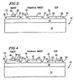
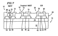
- a substrate 10 which in the preferred embodiment is a Separation by IMplantation of Oxygen (SIMOX) substrate, includes a silicon layer 12, which is a single crystal silicon, and an oxide layer 14.
- Oxide layer 14 has a thickness of between 100 nm and 300 nm.
- nMOS transistor 16 an n - channel snapback MOS transistor 18, and a p + /n/p/n + silicon-controlled rectifier (SCR) 20 are depicted.
- SCR silicon-controlled rectifier
- Other devices such as gate controlled diodes, zener diodes and bipolar transistors may also be constructed according to the method of the invention.
- the substrate is initially prepared by known techniques to form active areas which are isolated from one another. This may either be by a LOCOS, or a mesa structure.
- LOCOS is a local oxidation process used to isolate a device area.
- the structure depicted in Fig. 1 shows several active areas as such will appear following mesa isolation.
- n - silicon island 26 and p - silicon islands 22, 24, and 23 are arsenic ions which are implanted at an energy of between 10 keV and 50 keV, at a concentration of between 1 ⁇ 10 12 cm -2 and 5 ⁇ 10 13 cm -2 .
- BF 2 ions are implanted at an energy of between 10 keV and 40 keV, at a concentration of between 1 ⁇ 10 12 cm -2 and 5 ⁇ 10 13 cm -2 . This implantation takes place to provide proper threshold voltage of between 0.3 volts and 0.7 volts for MOS transistor fabrication. Additionally, this lays the ground work for the ESD protection of the devices in a subsequent step.
- gate oxidation provides an oxide layer 30, 32, and 34, also referred to herein as insulated areas, over the previously doped silicon islands.
- a layer of polysilicon is deposited by CVD and doped to form an n + area, which will ultimately become a gate electrode 36.
- phosphorous ions are implanted at an energy level of 40 keV and 120 keV, at a concentration of 1 ⁇ 10 15 cm -2 to 1 ⁇ 10 16 cm -2 .
- the polysilicon may be doped at the same time as source/drain ion implantation, which is a later step herein.
- the structure is covered with photoresist and etched to form gate electrode 36, after which, the photo resist is removed.
- the doped areas are also referred to herein as selectively conductive areas.
- oxide layer 38 is deposited by CVD and is anisotropically etched to form side wall oxide about polysilicon gate 36.
- Silicon layers 40, 42, and 44 are grown by selective epitaxial methods, which grows the silicon only onto other silicon and polysilicon layers. The newly grown layers of silicon are not doped.
- the next step in the formation of the ESD protected devices is diffusion. This is the only additional process step required for the ESD device fabrication of the invention.
- the structure is heated at a temperature of between 850° C to 1150° C from between 30 minutes to three hours. This redistributes the doping in silicon islands 22, 24, 26, and 28 into the epitaxial deposited silicon layers 40, 42, and 44, resulting in doped silicon areas 46, which is a combination of previously identified areas 22 and 40, area 48 which is a combination of previously identified areas 24 and 42, area 50 which is a combination of previously identified areas 26 and 44, and area 52 which is a combination of previously identified areas 28 and 44.
- the total dopant in the channel region will be on the order of 1 ⁇ 10 12 cm -2 . Therefore, if the dopant is uniformly distributed, the doping density of the top silicon and the epitaxial silicon layer will be on the order of 5 ⁇ 10 16 cm -3 to 10 ⁇ 10 17 cm -3 .
- an oxide layer 66 is deposited by CVD over the entire structure.
- the structure is covered with photoresist to provide the etching for contact holes and metalization, resulting in metal contacts 68, 70, 72, 74, 76, 78, and 80.
- the metal gate device has a single electrode connected to the gate and the source thereof.
- the current handling capacity of a pn junction of this structure is: 1 + T a p i T T a p S i times larger than the prior art structure.
- the current handling capacity of the device is 5 times larger than that of the prior art structure made on the same surface area.
- a thicker selective epitaxial layer may be used if larger protection or smaller ESD device area is required.
Landscapes
- Semiconductor Integrated Circuits (AREA)
- Metal-Oxide And Bipolar Metal-Oxide Semiconductor Integrated Circuits (AREA)
- Thin Film Transistor (AREA)
Claims (4)
- Verfahren zum Bilden einer ESD-geschützten Vorrichtung auf einem ultradünnen SOI-Substrat, mit den folgenden Schritten:Vorbereiten isolierter aktiver Bereiche auf einem Substrat (10), das eine Einkristall-Siliciumschicht (12) und eine Oxidschicht (14) auf der Einkristall-Siliciumschicht aufweist, Dotieren der isolierten aktiven Bereiche mit Dotierstoffen, um wahlweise leitende Bereiche (22, 24, 26, 28) in den isolierten aktiven Bereichen zu bilden, und Bilden von Oxidschichten (30, 32, 34) über den dotierten isolierten aktiven Bereichen;epitaktisches Aufwachsenlassen einer Siliciumschicht (40, 42, 44) auf den wahlweise leitenden Bereichen nach der Entfernung der Oxidschicht; undnach dem epitaktischen Aufwachsenlassen der Siliciumschicht Erhitzen des Substrats, um den Dotierstoff aus den dotierten, wahlweise leitenden Bereichen in die epitaktisch aufgewachsene Siliciumschicht umzuverteilen, was dotierte Siliciumbereiche (46, 48, 50, 52) ergibt, die eine Kombination aus den dotierten, wahlweise leitenden Bereichen und dem epitaktisch aufgewachsenen Silicium sind.
- Verfahren nach Anspruch 1, bei dem der Schritt des Erhitzens des Substrats das Erhitzen auf eine Temperatur im Bereich von 850 °C bis 1150 °C für eine Dauer im Bereich von 30 Minuten bis drei Stunden enthält.
- Verfahren nach Anspruch 2, bei dem das Dotieren der isolierten aktiven Bereiche des Substrats enthält: Implantieren von BF2-Ionen, um in den aktiven Bereichen leitende Bereiche des p-Typs zu bilden, mit einer Energie im Bereich von 10 keV bis 40 keV mit einer Dosis im Bereich von 1 · 1012 cm-2 bis 5 · 1013 cm-2, und bei dem der Schritt des Erhitzens des Substrats die Dotierstoffe so umverteilt, dass eine Dotierdichte von Ionen in den dotierten, wahlweise leitenden Bereichen und in den Bereichen der epitaktisch aufgewachsenen Siliciumschicht, die mit den implantierten Bereichen kombiniert sind, im Bereich von 5 · 1016 cm-3 bis 10·1017 cm-3 geschaffen wird.
- Verfahren nach Anspruch 2, bei dem das Dotieren der isolierten aktiven Bereiche des Substrats enthält: Implantieren von Arsenionen, um in den aktiven Bereichen leitende Bereiche des n-Typs zu bilden, mit einer Energie im Bereich von 10 keV bis 50 keV mit einer Dosis im Bereich von 1·1012 cm-2 bis 5 · 1013 cm-2, und bei dem der Schritt des Erhitzens des Substrats die Dotierstoffe so umverteilt, dass eine Dotierdichte von Ionen in den dotierten, wahlweise leitenden Bereichen und in den Bereichen der epitaktisch aufgewachsenen Siliciumschicht, die mit den implantierten Bereichen kombiniert sind, im Bereich von 5 · 1016 cm-3 bis 10 · 1017 cm-3 geschaffen wird.
Applications Claiming Priority (2)
| Application Number | Priority Date | Filing Date | Title |
|---|---|---|---|
| US82084 | 1998-05-20 | ||
| US09/082,084 US6080612A (en) | 1998-05-20 | 1998-05-20 | Method of forming an ultra-thin SOI electrostatic discharge protection device |
Publications (2)
| Publication Number | Publication Date |
|---|---|
| EP0959497A1 EP0959497A1 (de) | 1999-11-24 |
| EP0959497B1 true EP0959497B1 (de) | 2006-08-02 |
Family
ID=22168973
Family Applications (1)
| Application Number | Title | Priority Date | Filing Date |
|---|---|---|---|
| EP99302108A Expired - Lifetime EP0959497B1 (de) | 1998-05-20 | 1999-03-18 | Herstellungsverfahren für eine ultradünne, elektrostatische SOI-Entladungsschutzvorrichtung |
Country Status (6)
| Country | Link |
|---|---|
| US (1) | US6080612A (de) |
| EP (1) | EP0959497B1 (de) |
| JP (1) | JP3792930B2 (de) |
| KR (1) | KR100281397B1 (de) |
| DE (1) | DE69932564T2 (de) |
| TW (1) | TW407359B (de) |
Families Citing this family (6)
| Publication number | Priority date | Publication date | Assignee | Title |
|---|---|---|---|---|
| US6388289B1 (en) * | 1999-01-28 | 2002-05-14 | Oki Electric Industry Co., Ltd. | Semiconductor device having electrostatic discharge protection circuit |
| JP2001077368A (ja) * | 1999-09-03 | 2001-03-23 | Mitsubishi Electric Corp | 半導体装置及びその製造方法 |
| JP4573963B2 (ja) | 2000-08-08 | 2010-11-04 | ルネサスエレクトロニクス株式会社 | 半導体装置 |
| CN100452392C (zh) * | 2003-05-22 | 2009-01-14 | 统宝光电股份有限公司 | 具厚膜多晶硅的静电放电防护元件、电子装置及制造方法 |
| US6913959B2 (en) * | 2003-06-23 | 2005-07-05 | Advanced Micro Devices, Inc. | Method of manufacturing a semiconductor device having a MESA structure |
| CN114361256B (zh) * | 2021-12-28 | 2025-09-02 | 中国电子产品可靠性与环境试验研究所((工业和信息化部电子第五研究所)(中国赛宝实验室)) | 二极管结构及其制备方法、半导体器件结构及其制备方法 |
Family Cites Families (10)
| Publication number | Priority date | Publication date | Assignee | Title |
|---|---|---|---|---|
| DE3476295D1 (en) * | 1983-09-19 | 1989-02-23 | Fairchild Semiconductor | Method of manufacturing transistor structures having junctions bound by insulating layers, and resulting structures |
| JPH0738435B2 (ja) * | 1986-06-13 | 1995-04-26 | 松下電器産業株式会社 | 半導体装置の製造方法 |
| US5930638A (en) * | 1993-07-12 | 1999-07-27 | Peregrine Semiconductor Corp. | Method of making a low parasitic resistor on ultrathin silicon on insulator |
| KR0142797B1 (ko) * | 1994-06-17 | 1998-08-17 | 문정환 | 실리콘-온-인슐레이터구조의 제조방법 |
| US5889315A (en) * | 1994-08-18 | 1999-03-30 | National Semiconductor Corporation | Semiconductor structure having two levels of buried regions |
| US5610790A (en) * | 1995-01-20 | 1997-03-11 | Xilinx, Inc. | Method and structure for providing ESD protection for silicon on insulator integrated circuits |
| KR100331296B1 (ko) * | 1995-12-20 | 2002-06-20 | 클라크 3세 존 엠. | 에피택셜 핀치 저항기 및 그 형성 방법 |
| FR2746544B1 (fr) * | 1996-03-20 | 1998-05-15 | Commissariat Energie Atomique | Substrat de type silicium sur isolant pour la fabrication de transistors et procede de preparation d'un tel substrat |
| FR2756104B1 (fr) * | 1996-11-19 | 1999-01-29 | Sgs Thomson Microelectronics | Fabrication de circuits integres bipolaires/cmos |
| FR2758004B1 (fr) * | 1996-12-27 | 1999-03-05 | Sgs Thomson Microelectronics | Transistor bipolaire a isolement dielectrique |
-
1998
- 1998-05-20 US US09/082,084 patent/US6080612A/en not_active Expired - Fee Related
-
1999
- 1999-02-24 JP JP04721299A patent/JP3792930B2/ja not_active Expired - Fee Related
- 1999-03-16 TW TW088104066A patent/TW407359B/zh active
- 1999-03-18 EP EP99302108A patent/EP0959497B1/de not_active Expired - Lifetime
- 1999-03-18 DE DE69932564T patent/DE69932564T2/de not_active Expired - Fee Related
- 1999-03-31 KR KR1019990011184A patent/KR100281397B1/ko not_active Expired - Fee Related
Also Published As
| Publication number | Publication date |
|---|---|
| KR19990087887A (ko) | 1999-12-27 |
| JPH11330439A (ja) | 1999-11-30 |
| DE69932564D1 (de) | 2006-09-14 |
| EP0959497A1 (de) | 1999-11-24 |
| JP3792930B2 (ja) | 2006-07-05 |
| US6080612A (en) | 2000-06-27 |
| KR100281397B1 (ko) | 2001-02-01 |
| TW407359B (en) | 2000-10-01 |
| DE69932564T2 (de) | 2007-10-25 |
Similar Documents
| Publication | Publication Date | Title |
|---|---|---|
| US5424572A (en) | Spacer formation in a semiconductor structure | |
| US5359219A (en) | Silicon on insulator device comprising improved substrate doping | |
| US5627097A (en) | Method for making CMOS device having reduced parasitic capacitance | |
| US5326710A (en) | Process for fabricating lateral PNP transistor structure and BICMOS IC | |
| EP0224717B1 (de) | Selbstalignierter Kanalunterbrecher | |
| US7557393B2 (en) | JFET with built in back gate in either SOI or bulk silicon | |
| KR100199465B1 (ko) | 반도체 디바이스용으로 제조되는 접점구조물 및 이를 제조하는 방법 | |
| EP0975023B1 (de) | Verfahren zur Herstellung von gegen elektrostatische Entladung geschützten Bauelementen mit selbstausgerichteter Silicidstruktur | |
| US20030080394A1 (en) | Control of dopant diffusion from polysilicon emitters in bipolar integrated circuits | |
| US20020117714A1 (en) | High voltage MOS transistor | |
| EP0421507B1 (de) | Verfahren zur Herstellung eines bipolaren Transistors | |
| EP0959497B1 (de) | Herstellungsverfahren für eine ultradünne, elektrostatische SOI-Entladungsschutzvorrichtung | |
| US5010034A (en) | CMOS and bipolar fabrication process using selective epitaxial growth scalable to below 0.5 micron | |
| EP0489262A1 (de) | Lateraler Bipolartransistor mit seitlich geführtem Basiskontakt und dessen Herstellungsverfahren | |
| US6774455B2 (en) | Semiconductor device with a collector contact in a depressed well-region | |
| US5719423A (en) | Isolated power transistor | |
| US4943536A (en) | Transistor isolation | |
| US6806159B2 (en) | Method for manufacturing a semiconductor device with sinker contact region | |
| EP0434182B1 (de) | Verfahren zur Herstellung vergrabener Zonen für integrierte Schaltungen | |
| JPH06224381A (ja) | Cmosトランジスタ用nmos低濃度ドレーンpmosハローicプロセス | |
| US7164186B2 (en) | Structure of semiconductor device with sinker contact region | |
| JP2931243B2 (ja) | 半導体素子の製造方法 | |
| KR100200058B1 (ko) | 반전 주입물을 분리시키는 방법 | |
| EP0961316A2 (de) | Verfahren zur Herstellung eines integrierten, vertikalen Bipolartransistors | |
| EP0477683A2 (de) | Verfahren zum Herstellen einer CMOS Struktur |
Legal Events
| Date | Code | Title | Description |
|---|---|---|---|
| PUAI | Public reference made under article 153(3) epc to a published international application that has entered the european phase |
Free format text: ORIGINAL CODE: 0009012 |
|
| AK | Designated contracting states |
Kind code of ref document: A1 Designated state(s): DE FR GB |
|
| AX | Request for extension of the european patent |
Free format text: AL;LT;LV;MK;RO;SI |
|
| 17P | Request for examination filed |
Effective date: 20000330 |
|
| AKX | Designation fees paid |
Free format text: DE FR GB |
|
| 17Q | First examination report despatched |
Effective date: 20030606 |
|
| GRAP | Despatch of communication of intention to grant a patent |
Free format text: ORIGINAL CODE: EPIDOSNIGR1 |
|
| GRAC | Information related to communication of intention to grant a patent modified |
Free format text: ORIGINAL CODE: EPIDOSCIGR1 |
|
| GRAS | Grant fee paid |
Free format text: ORIGINAL CODE: EPIDOSNIGR3 |
|
| GRAA | (expected) grant |
Free format text: ORIGINAL CODE: 0009210 |
|
| AK | Designated contracting states |
Kind code of ref document: B1 Designated state(s): DE FR GB |
|
| REG | Reference to a national code |
Ref country code: GB Ref legal event code: FG4D |
|
| REF | Corresponds to: |
Ref document number: 69932564 Country of ref document: DE Date of ref document: 20060914 Kind code of ref document: P |
|
| ET | Fr: translation filed | ||
| PLBE | No opposition filed within time limit |
Free format text: ORIGINAL CODE: 0009261 |
|
| STAA | Information on the status of an ep patent application or granted ep patent |
Free format text: STATUS: NO OPPOSITION FILED WITHIN TIME LIMIT |
|
| 26N | No opposition filed |
Effective date: 20070503 |
|
| PGFP | Annual fee paid to national office [announced via postgrant information from national office to epo] |
Ref country code: GB Payment date: 20090318 Year of fee payment: 11 |
|
| PGFP | Annual fee paid to national office [announced via postgrant information from national office to epo] |
Ref country code: DE Payment date: 20090313 Year of fee payment: 11 |
|
| PGFP | Annual fee paid to national office [announced via postgrant information from national office to epo] |
Ref country code: FR Payment date: 20090316 Year of fee payment: 11 |
|
| GBPC | Gb: european patent ceased through non-payment of renewal fee |
Effective date: 20100318 |
|
| REG | Reference to a national code |
Ref country code: FR Ref legal event code: ST Effective date: 20101130 |
|
| PG25 | Lapsed in a contracting state [announced via postgrant information from national office to epo] |
Ref country code: FR Free format text: LAPSE BECAUSE OF NON-PAYMENT OF DUE FEES Effective date: 20100331 |
|
| PG25 | Lapsed in a contracting state [announced via postgrant information from national office to epo] |
Ref country code: DE Free format text: LAPSE BECAUSE OF NON-PAYMENT OF DUE FEES Effective date: 20101001 |
|
| PG25 | Lapsed in a contracting state [announced via postgrant information from national office to epo] |
Ref country code: GB Free format text: LAPSE BECAUSE OF NON-PAYMENT OF DUE FEES Effective date: 20100318 |