EP0959505A2 - Procédé pour aplanir la topographie dans un capteur d'image - Google Patents
Procédé pour aplanir la topographie dans un capteur d'image Download PDFInfo
- Publication number
- EP0959505A2 EP0959505A2 EP99201426A EP99201426A EP0959505A2 EP 0959505 A2 EP0959505 A2 EP 0959505A2 EP 99201426 A EP99201426 A EP 99201426A EP 99201426 A EP99201426 A EP 99201426A EP 0959505 A2 EP0959505 A2 EP 0959505A2
- Authority
- EP
- European Patent Office
- Prior art keywords
- layer
- transparent
- photoactive area
- patterning
- photosensitive layer
- Prior art date
- Legal status (The legal status is an assumption and is not a legal conclusion. Google has not performed a legal analysis and makes no representation as to the accuracy of the status listed.)
- Withdrawn
Links
- 238000000034 method Methods 0.000 title claims abstract description 52
- 239000007787 solid Substances 0.000 title claims abstract description 18
- 238000012876 topography Methods 0.000 title abstract description 11
- 238000000059 patterning Methods 0.000 claims abstract description 35
- 238000011161 development Methods 0.000 claims abstract description 34
- 239000011248 coating agent Substances 0.000 claims abstract description 32
- 238000000576 coating method Methods 0.000 claims abstract description 32
- 230000003213 activating effect Effects 0.000 claims abstract description 22
- 238000003384 imaging method Methods 0.000 claims abstract description 15
- 239000004065 semiconductor Substances 0.000 claims abstract description 15
- 229920000642 polymer Polymers 0.000 claims description 26
- 230000005855 radiation Effects 0.000 claims description 5
- 238000010438 heat treatment Methods 0.000 claims 1
- 239000000758 substrate Substances 0.000 abstract description 13
- 230000008569 process Effects 0.000 abstract description 10
- 229910052751 metal Inorganic materials 0.000 abstract description 6
- 239000002184 metal Substances 0.000 abstract description 6
- 230000018109 developmental process Effects 0.000 description 27
- 239000000463 material Substances 0.000 description 13
- 238000004519 manufacturing process Methods 0.000 description 12
- -1 poly(vinyl cinnamate) Polymers 0.000 description 12
- 108010010803 Gelatin Proteins 0.000 description 9
- 229920000159 gelatin Polymers 0.000 description 9
- 239000008273 gelatin Substances 0.000 description 9
- 235000019322 gelatine Nutrition 0.000 description 9
- 235000011852 gelatine desserts Nutrition 0.000 description 9
- 238000004090 dissolution Methods 0.000 description 6
- 229920002120 photoresistant polymer Polymers 0.000 description 6
- 238000000151 deposition Methods 0.000 description 5
- 238000011049 filling Methods 0.000 description 5
- 239000000203 mixture Substances 0.000 description 5
- 239000011230 binding agent Substances 0.000 description 4
- 230000008859 change Effects 0.000 description 4
- 239000000084 colloidal system Substances 0.000 description 4
- 238000004132 cross linking Methods 0.000 description 4
- 239000012954 diazonium Substances 0.000 description 4
- 150000001989 diazonium salts Chemical class 0.000 description 4
- 239000000178 monomer Substances 0.000 description 4
- 239000002904 solvent Substances 0.000 description 4
- 239000000126 substance Substances 0.000 description 4
- XLYOFNOQVPJJNP-UHFFFAOYSA-N water Substances O XLYOFNOQVPJJNP-UHFFFAOYSA-N 0.000 description 4
- 238000013459 approach Methods 0.000 description 3
- 238000003491 array Methods 0.000 description 3
- 239000002585 base Substances 0.000 description 3
- 150000001875 compounds Chemical class 0.000 description 3
- 230000006870 function Effects 0.000 description 3
- 238000009499 grossing Methods 0.000 description 3
- 238000005498 polishing Methods 0.000 description 3
- 238000006116 polymerization reaction Methods 0.000 description 3
- 238000000926 separation method Methods 0.000 description 3
- 238000004528 spin coating Methods 0.000 description 3
- AZQWKYJCGOJGHM-UHFFFAOYSA-N 1,4-benzoquinone Chemical compound O=C1C=CC(=O)C=C1 AZQWKYJCGOJGHM-UHFFFAOYSA-N 0.000 description 2
- NGNBDVOYPDDBFK-UHFFFAOYSA-N 2-[2,4-di(pentan-2-yl)phenoxy]acetyl chloride Chemical compound CCCC(C)C1=CC=C(OCC(Cl)=O)C(C(C)CCC)=C1 NGNBDVOYPDDBFK-UHFFFAOYSA-N 0.000 description 2
- IJGRMHOSHXDMSA-UHFFFAOYSA-N Atomic nitrogen Chemical compound N#N IJGRMHOSHXDMSA-UHFFFAOYSA-N 0.000 description 2
- 241001428800 Cell fusing agent virus Species 0.000 description 2
- XUIMIQQOPSSXEZ-UHFFFAOYSA-N Silicon Chemical group [Si] XUIMIQQOPSSXEZ-UHFFFAOYSA-N 0.000 description 2
- 150000001540 azides Chemical class 0.000 description 2
- 125000002091 cationic group Chemical group 0.000 description 2
- 229920002678 cellulose Polymers 0.000 description 2
- 239000003795 chemical substances by application Substances 0.000 description 2
- 230000008021 deposition Effects 0.000 description 2
- SOCTUWSJJQCPFX-UHFFFAOYSA-N dichromate(2-) Chemical class [O-][Cr](=O)(=O)O[Cr]([O-])(=O)=O SOCTUWSJJQCPFX-UHFFFAOYSA-N 0.000 description 2
- 239000000975 dye Substances 0.000 description 2
- 238000005530 etching Methods 0.000 description 2
- 239000000945 filler Substances 0.000 description 2
- 238000009472 formulation Methods 0.000 description 2
- 239000003999 initiator Substances 0.000 description 2
- 208000036971 interstitial lung disease 2 Diseases 0.000 description 2
- 230000004048 modification Effects 0.000 description 2
- 238000012986 modification Methods 0.000 description 2
- 229920003986 novolac Polymers 0.000 description 2
- 238000002161 passivation Methods 0.000 description 2
- 229920002451 polyvinyl alcohol Polymers 0.000 description 2
- 238000012545 processing Methods 0.000 description 2
- 235000018102 proteins Nutrition 0.000 description 2
- 108090000623 proteins and genes Proteins 0.000 description 2
- 102000004169 proteins and genes Human genes 0.000 description 2
- 150000003254 radicals Chemical class 0.000 description 2
- 229910052710 silicon Inorganic materials 0.000 description 2
- 239000010703 silicon Substances 0.000 description 2
- 239000000243 solution Substances 0.000 description 2
- CDSULTPOCMWJCM-UHFFFAOYSA-N 4h-chromene-2,3-dione Chemical class C1=CC=C2OC(=O)C(=O)CC2=C1 CDSULTPOCMWJCM-UHFFFAOYSA-N 0.000 description 1
- 244000215068 Acacia senegal Species 0.000 description 1
- 229920001817 Agar Polymers 0.000 description 1
- 102000009027 Albumins Human genes 0.000 description 1
- 108010088751 Albumins Proteins 0.000 description 1
- 102000008186 Collagen Human genes 0.000 description 1
- 108010035532 Collagen Proteins 0.000 description 1
- RWSOTUBLDIXVET-UHFFFAOYSA-N Dihydrogen sulfide Chemical class S RWSOTUBLDIXVET-UHFFFAOYSA-N 0.000 description 1
- 241000206672 Gelidium Species 0.000 description 1
- 229920000084 Gum arabic Polymers 0.000 description 1
- DGAQECJNVWCQMB-PUAWFVPOSA-M Ilexoside XXIX Chemical compound C[C@@H]1CC[C@@]2(CC[C@@]3(C(=CC[C@H]4[C@]3(CC[C@@H]5[C@@]4(CC[C@@H](C5(C)C)OS(=O)(=O)[O-])C)C)[C@@H]2[C@]1(C)O)C)C(=O)O[C@H]6[C@@H]([C@H]([C@@H]([C@H](O6)CO)O)O)O.[Na+] DGAQECJNVWCQMB-PUAWFVPOSA-M 0.000 description 1
- 244000151018 Maranta arundinacea Species 0.000 description 1
- 235000010804 Maranta arundinacea Nutrition 0.000 description 1
- WHNWPMSKXPGLAX-UHFFFAOYSA-N N-Vinyl-2-pyrrolidone Chemical compound C=CN1CCCC1=O WHNWPMSKXPGLAX-UHFFFAOYSA-N 0.000 description 1
- 239000004793 Polystyrene Substances 0.000 description 1
- 239000004372 Polyvinyl alcohol Substances 0.000 description 1
- ZLMJMSJWJFRBEC-UHFFFAOYSA-N Potassium Chemical compound [K] ZLMJMSJWJFRBEC-UHFFFAOYSA-N 0.000 description 1
- 206010070834 Sensitisation Diseases 0.000 description 1
- 244000028419 Styrax benzoin Species 0.000 description 1
- 235000000126 Styrax benzoin Nutrition 0.000 description 1
- 235000008411 Sumatra benzointree Nutrition 0.000 description 1
- 235000012419 Thalia geniculata Nutrition 0.000 description 1
- 229920002494 Zein Polymers 0.000 description 1
- 239000000205 acacia gum Substances 0.000 description 1
- 235000010489 acacia gum Nutrition 0.000 description 1
- 239000002253 acid Substances 0.000 description 1
- 150000001252 acrylic acid derivatives Chemical class 0.000 description 1
- 238000007259 addition reaction Methods 0.000 description 1
- 235000010419 agar Nutrition 0.000 description 1
- 239000003513 alkali Substances 0.000 description 1
- 150000001412 amines Chemical group 0.000 description 1
- JOSWYUNQBRPBDN-UHFFFAOYSA-P ammonium dichromate Chemical compound [NH4+].[NH4+].[O-][Cr](=O)(=O)O[Cr]([O-])(=O)=O JOSWYUNQBRPBDN-UHFFFAOYSA-P 0.000 description 1
- 239000007864 aqueous solution Substances 0.000 description 1
- 238000010420 art technique Methods 0.000 description 1
- 125000000751 azo group Chemical group [*]N=N[*] 0.000 description 1
- 229960002130 benzoin Drugs 0.000 description 1
- 230000015572 biosynthetic process Effects 0.000 description 1
- 239000008280 blood Substances 0.000 description 1
- 210000004369 blood Anatomy 0.000 description 1
- 238000010504 bond cleavage reaction Methods 0.000 description 1
- 239000005018 casein Substances 0.000 description 1
- BECPQYXYKAMYBN-UHFFFAOYSA-N casein, tech. Chemical compound NCCCCC(C(O)=O)N=C(O)C(CC(O)=O)N=C(O)C(CCC(O)=N)N=C(O)C(CC(C)C)N=C(O)C(CCC(O)=O)N=C(O)C(CC(O)=O)N=C(O)C(CCC(O)=O)N=C(O)C(C(C)O)N=C(O)C(CCC(O)=N)N=C(O)C(CCC(O)=N)N=C(O)C(CCC(O)=N)N=C(O)C(CCC(O)=O)N=C(O)C(CCC(O)=O)N=C(O)C(COP(O)(O)=O)N=C(O)C(CCC(O)=N)N=C(O)C(N)CC1=CC=CC=C1 BECPQYXYKAMYBN-UHFFFAOYSA-N 0.000 description 1
- 235000021240 caseins Nutrition 0.000 description 1
- 238000010538 cationic polymerization reaction Methods 0.000 description 1
- 150000001768 cations Chemical class 0.000 description 1
- 239000001913 cellulose Substances 0.000 description 1
- 229940114081 cinnamate Drugs 0.000 description 1
- 229920001436 collagen Polymers 0.000 description 1
- 239000004020 conductor Substances 0.000 description 1
- 238000010276 construction Methods 0.000 description 1
- 230000007423 decrease Effects 0.000 description 1
- 230000007547 defect Effects 0.000 description 1
- 230000001419 dependent effect Effects 0.000 description 1
- ISAOCJYIOMOJEB-UHFFFAOYSA-N desyl alcohol Natural products C=1C=CC=CC=1C(O)C(=O)C1=CC=CC=C1 ISAOCJYIOMOJEB-UHFFFAOYSA-N 0.000 description 1
- 125000000664 diazo group Chemical group [N-]=[N+]=[*] 0.000 description 1
- IJGRMHOSHXDMSA-UHFFFAOYSA-O diazynium Chemical compound [NH+]#N IJGRMHOSHXDMSA-UHFFFAOYSA-O 0.000 description 1
- 238000006471 dimerization reaction Methods 0.000 description 1
- 238000005516 engineering process Methods 0.000 description 1
- 150000002118 epoxides Chemical class 0.000 description 1
- 239000012949 free radical photoinitiator Substances 0.000 description 1
- 150000004676 glycans Chemical class 0.000 description 1
- 235000019382 gum benzoic Nutrition 0.000 description 1
- 244000144980 herd Species 0.000 description 1
- 238000005213 imbibition Methods 0.000 description 1
- 230000006872 improvement Effects 0.000 description 1
- 238000003780 insertion Methods 0.000 description 1
- 230000037431 insertion Effects 0.000 description 1
- 239000012212 insulator Substances 0.000 description 1
- 238000002955 isolation Methods 0.000 description 1
- 239000011159 matrix material Substances 0.000 description 1
- 230000007246 mechanism Effects 0.000 description 1
- 150000002734 metacrylic acid derivatives Chemical class 0.000 description 1
- GNWCSWUWMHQEMD-UHFFFAOYSA-N naphthalene-1,2-dione diazide Chemical compound [N-]=[N+]=[N-].[N-]=[N+]=[N-].C1=CC=C2C(=O)C(=O)C=CC2=C1 GNWCSWUWMHQEMD-UHFFFAOYSA-N 0.000 description 1
- 229910052757 nitrogen Inorganic materials 0.000 description 1
- 239000001814 pectin Substances 0.000 description 1
- 229920001277 pectin Polymers 0.000 description 1
- 235000010987 pectin Nutrition 0.000 description 1
- 150000002978 peroxides Chemical class 0.000 description 1
- 238000006349 photocyclization reaction Methods 0.000 description 1
- 238000011907 photodimerization Methods 0.000 description 1
- 229920003229 poly(methyl methacrylate) Polymers 0.000 description 1
- 229920001195 polyisoprene Polymers 0.000 description 1
- 229920005596 polymer binder Polymers 0.000 description 1
- 239000002491 polymer binding agent Substances 0.000 description 1
- 239000004926 polymethyl methacrylate Substances 0.000 description 1
- 229920001282 polysaccharide Polymers 0.000 description 1
- 239000005017 polysaccharide Substances 0.000 description 1
- 229920002223 polystyrene Polymers 0.000 description 1
- 229910052700 potassium Inorganic materials 0.000 description 1
- 239000011591 potassium Substances 0.000 description 1
- 125000002924 primary amino group Chemical group [H]N([H])* 0.000 description 1
- 150000003242 quaternary ammonium salts Chemical class 0.000 description 1
- 230000009467 reduction Effects 0.000 description 1
- 230000007261 regionalization Effects 0.000 description 1
- 229920005989 resin Polymers 0.000 description 1
- 239000011347 resin Substances 0.000 description 1
- 230000027756 respiratory electron transport chain Effects 0.000 description 1
- 230000007017 scission Effects 0.000 description 1
- 230000008313 sensitization Effects 0.000 description 1
- 229910052708 sodium Inorganic materials 0.000 description 1
- 239000011734 sodium Substances 0.000 description 1
- 230000006641 stabilisation Effects 0.000 description 1
- 238000011105 stabilization Methods 0.000 description 1
- WBYWAXJHAXSJNI-VOTSOKGWSA-M trans-cinnamate Chemical compound [O-]C(=O)\C=C\C1=CC=CC=C1 WBYWAXJHAXSJNI-VOTSOKGWSA-M 0.000 description 1
- 238000001429 visible spectrum Methods 0.000 description 1
- 229920003169 water-soluble polymer Polymers 0.000 description 1
- 239000005019 zein Substances 0.000 description 1
- 229940093612 zein Drugs 0.000 description 1
Images
Classifications
-
- H—ELECTRICITY
- H10—SEMICONDUCTOR DEVICES; ELECTRIC SOLID-STATE DEVICES NOT OTHERWISE PROVIDED FOR
- H10F—INORGANIC SEMICONDUCTOR DEVICES SENSITIVE TO INFRARED RADIATION, LIGHT, ELECTROMAGNETIC RADIATION OF SHORTER WAVELENGTH OR CORPUSCULAR RADIATION
- H10F77/00—Constructional details of devices covered by this subclass
- H10F77/30—Coatings
- H10F77/306—Coatings for devices having potential barriers
Definitions
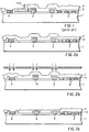
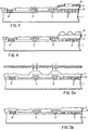
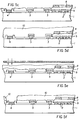
- the object of this invention is to simplify the previously discussed prior art processes for reducing the topography within a solid state imager by using a single coat, expose, and development sequence to produce a transparent layer that fills in the topographic features surrounding the photoactive area (i.e., metal wiring) while also planarizing the photoactive area.
- planarizing layer 7 Various options exist for completion of the planarizing layer. More specifically, the materials chosen for use as the planarizing layer 7 and the process employed for opening the device bonding pads 4 for connection to external electronic circuitry dictates the procedure to follow. Thus, for example, it may be advantageous to generate openings down to the bonding pads 4, particularly if the planarizing layer is a photosensitive composition or if a photoresist is coated upon the planarizing layer. Materials useful in the former include formulations capable of photoinitiated polymerization, photocrosslinking, photodimerization, light induced scission and photofunctional change. In each case, the patternwise exposure of the coating creates differences in the dissolution properties of the coating.
- Still another class of materials suitable for use as a planarizing layer are the photoinitiated polymerization imaging systems.
- light is absorbed by a compound which breaks down to form a reactive species which initiates the polymerization of monomers.
- These initiators are typically chosen to produce either a free radical or a cation.
- the free radical rapidly polymerizes acrylates and methacrylates to yield a high polymer. Since the monomer dissolves in many more solvents than the polymer and does so rapidly, a negative image mask is obtained after exposure and development. Cationic polymerization of epoxides yield the same results.
- Suitable free radical photoinitiators for this purpose include peroxides, azo compounds, benzoin ethers and ketocoumarins with amino accelerators.
- Positive imagable systems which become more soluble in the developer upon exposure, may also be used as planarizing layer. These systems function in accordance with one of two mechanisms, namely, photofunctional change or scissioning.
- poly(methyl methacrylate) is a polymer which undergoes scissioning during exposure at an appropriate wavelength. In this process, the polymer backbone is broken, so reducing the molecular weight of the polymer. Since the dissolution rate for a polymer composition varies significantly and inversely with the molecular weight of the polymer, the rate of dissolution increases as the molecular weight decreases. Accordingly, during the development sequence, the exposed areas are removed rapidly to yield a positive image.
- Other scissioning polymers include poly(methylisopropenylketone), poly(dimethylglutarimide) and poly(nonafluorobutyl-methacrylate).
- Suitable hydrophillic colloids for this purpose include substances such as proteins, protein derivatives, cellulose derivatives and polysaccharides such as cellulose esters, gelatin (alkali or acid treated), gelatin derivatives such as acetylated gelatin and phthalated gelatin, dextren, gum arabic, zein, casein, pectin, collagen derivatives, collodion, agar-agar, arrowroot and albumin, all generally known to be useful as binders in photographic elements.
- the hydrophillic colloid, preferably gelatin or a gelatin derivative can be conveniently employed in combination with a dichromate salt, employed as a radiation responsive hardening agent.
- the dichromate salt is, for example, potassium, sodium or ammonium dichromate.
- the transparent patternable planarizing layer 7 can be removed from the bond pads either before or after CFA fabrication.
- the transparent patternable planarizing layer 7 can also be removed from the scribe area if desired. This can be done either before or after CFA fabrication.
- a second preferred processing sequence in accordance with the present invention shown in Figure 5a through 5f, may be used.
Landscapes
- Solid State Image Pick-Up Elements (AREA)
Applications Claiming Priority (2)
| Application Number | Priority Date | Filing Date | Title |
|---|---|---|---|
| US80849 | 1993-06-24 | ||
| US8084998A | 1998-05-18 | 1998-05-18 |
Publications (2)
| Publication Number | Publication Date |
|---|---|
| EP0959505A2 true EP0959505A2 (fr) | 1999-11-24 |
| EP0959505A3 EP0959505A3 (fr) | 2000-01-26 |
Family
ID=22160025
Family Applications (1)
| Application Number | Title | Priority Date | Filing Date |
|---|---|---|---|
| EP99201426A Withdrawn EP0959505A3 (fr) | 1998-05-18 | 1999-05-06 | Procédé pour aplanir la topographie dans un capteur d'image |
Country Status (2)
| Country | Link |
|---|---|
| EP (1) | EP0959505A3 (fr) |
| JP (1) | JP2000031448A (fr) |
Cited By (2)
| Publication number | Priority date | Publication date | Assignee | Title |
|---|---|---|---|---|
| US6849533B2 (en) * | 2003-01-29 | 2005-02-01 | Taiwan Semiconductor Manufacturing Co., Ltd | Method for fabricating microelectronic product with attenuated bond pad corrosion |
| US7799491B2 (en) | 2006-04-07 | 2010-09-21 | Aptina Imaging Corp. | Color filter array and imaging device containing such color filter array and method of fabrication |
Families Citing this family (1)
| Publication number | Priority date | Publication date | Assignee | Title |
|---|---|---|---|---|
| US6344369B1 (en) * | 2000-07-03 | 2002-02-05 | Taiwan Semiconductor Manufacturing Company | Method of protecting a bond pad structure, of a color image sensor cell, during a color filter fabrication process |
Family Cites Families (5)
| Publication number | Priority date | Publication date | Assignee | Title |
|---|---|---|---|---|
| KR920005444B1 (ko) * | 1989-12-02 | 1992-07-04 | 삼성전자 주식회사 | 칼라필터 및 그 제조방법 |
| JPH04334056A (ja) * | 1991-05-09 | 1992-11-20 | Toshiba Corp | 固体撮像装置の製造方法 |
| KR950011567B1 (ko) * | 1992-02-21 | 1995-10-06 | 삼성전자주식회사 | 칼라필터 제조방법 |
| US5654202A (en) * | 1992-03-24 | 1997-08-05 | Eastman Kodak Company | Stabilization of a patterned planarizing layer for solid state imagers prior to color filter pattern formation |
| JPH05299625A (ja) * | 1992-04-21 | 1993-11-12 | Mitsubishi Electric Corp | 固体撮像素子およびその製造方法 |
-
1999
- 1999-05-06 EP EP99201426A patent/EP0959505A3/fr not_active Withdrawn
- 1999-05-18 JP JP11136802A patent/JP2000031448A/ja active Pending
Cited By (2)
| Publication number | Priority date | Publication date | Assignee | Title |
|---|---|---|---|---|
| US6849533B2 (en) * | 2003-01-29 | 2005-02-01 | Taiwan Semiconductor Manufacturing Co., Ltd | Method for fabricating microelectronic product with attenuated bond pad corrosion |
| US7799491B2 (en) | 2006-04-07 | 2010-09-21 | Aptina Imaging Corp. | Color filter array and imaging device containing such color filter array and method of fabrication |
Also Published As
| Publication number | Publication date |
|---|---|
| EP0959505A3 (fr) | 2000-01-26 |
| JP2000031448A (ja) | 2000-01-28 |
Similar Documents
| Publication | Publication Date | Title |
|---|---|---|
| JP2863422B2 (ja) | 固体撮像装置およびその製造方法 | |
| US5654202A (en) | Stabilization of a patterned planarizing layer for solid state imagers prior to color filter pattern formation | |
| EP0035886A2 (fr) | Dispositif de formation d'images à l'état solide comportant un filtre à couleur matriciel et procédé pour sa fabrication | |
| JPH04359472A (ja) | マイクロレンズ形成方法 | |
| JPH04234706A (ja) | フィルター、それの製造方法およびそれを使用した固体イメージ装置 | |
| US4553153A (en) | Planarizing layer for semiconductor substrates such as solid state imagers | |
| US5286605A (en) | Method for producing solid-state imaging device | |
| JP3711211B2 (ja) | 固体撮像装置 | |
| US5135891A (en) | Method for forming film of uniform thickness on semiconductor substrate having concave portion | |
| EP0959505A2 (fr) | Procédé pour aplanir la topographie dans un capteur d'image | |
| JPH0624232B2 (ja) | 固体撮像装置の製造方法 | |
| JP2892865B2 (ja) | 固体撮像素子の製造方法 | |
| JPH06209094A (ja) | 固体撮像装置およびその製造方法 | |
| JP2786647B2 (ja) | カラー固体撮像装置の製造方法 | |
| JP2614064B2 (ja) | 固体カラー撮像素子 | |
| JPH05299625A (ja) | 固体撮像素子およびその製造方法 | |
| JPS6318341B2 (fr) | ||
| EP0434273B1 (fr) | Elément de filtrage de radiation électromagnétique et méthode de fabrication | |
| JP2702196B2 (ja) | カラー固体撮像素子およびその製造方法 | |
| JPS60103342A (ja) | カラ−フイルタ用レジスト組成物 | |
| JPS6251504B2 (fr) | ||
| JPS61296763A (ja) | カラ−固体撮像装置の製造方法 | |
| JPH02306660A (ja) | 固体撮像装置の製造方法 | |
| JPH09260623A (ja) | 固体撮像素子 | |
| KR0147642B1 (ko) | 반도체 장치의 미세 패턴 형성 방법 |
Legal Events
| Date | Code | Title | Description |
|---|---|---|---|
| PUAI | Public reference made under article 153(3) epc to a published international application that has entered the european phase |
Free format text: ORIGINAL CODE: 0009012 |
|
| AK | Designated contracting states |
Kind code of ref document: A2 Designated state(s): AT BE CH CY DE DK ES FI FR GB GR IE IT LI LU MC NL PT SE |
|
| AX | Request for extension of the european patent |
Free format text: AL;LT;LV;MK;RO;SI |
|
| PUAL | Search report despatched |
Free format text: ORIGINAL CODE: 0009013 |
|
| AK | Designated contracting states |
Kind code of ref document: A3 Designated state(s): AT BE CH CY DE DK ES FI FR GB GR IE IT LI LU MC NL PT SE |
|
| AX | Request for extension of the european patent |
Free format text: AL;LT;LV;MK;RO;SI |
|
| AKX | Designation fees paid | ||
| STAA | Information on the status of an ep patent application or granted ep patent |
Free format text: STATUS: THE APPLICATION IS DEEMED TO BE WITHDRAWN |
|
| 18D | Application deemed to be withdrawn |
Effective date: 20000727 |
|
| REG | Reference to a national code |
Ref country code: DE Ref legal event code: 8566 |