EP0959564A1 - Dispositif résistif à commande linéaire - Google Patents
Dispositif résistif à commande linéaire Download PDFInfo
- Publication number
- EP0959564A1 EP0959564A1 EP19990303634 EP99303634A EP0959564A1 EP 0959564 A1 EP0959564 A1 EP 0959564A1 EP 19990303634 EP19990303634 EP 19990303634 EP 99303634 A EP99303634 A EP 99303634A EP 0959564 A1 EP0959564 A1 EP 0959564A1
- Authority
- EP
- European Patent Office
- Prior art keywords
- pull
- transistor
- resistor
- output
- data
- Prior art date
- Legal status (The legal status is an assumption and is not a legal conclusion. Google has not performed a legal analysis and makes no representation as to the accuracy of the status listed.)
- Withdrawn
Links
- 239000000872 buffer Substances 0.000 claims abstract description 40
- 238000010586 diagram Methods 0.000 description 12
- 230000005540 biological transmission Effects 0.000 description 5
- 238000000034 method Methods 0.000 description 4
- 239000008186 active pharmaceutical agent Substances 0.000 description 2
- 238000012512 characterization method Methods 0.000 description 2
- 230000000295 complement effect Effects 0.000 description 1
- 230000001419 dependent effect Effects 0.000 description 1
- 230000000694 effects Effects 0.000 description 1
- 230000001939 inductive effect Effects 0.000 description 1
- 229910044991 metal oxide Inorganic materials 0.000 description 1
- 150000004706 metal oxides Chemical class 0.000 description 1
- 239000004065 semiconductor Substances 0.000 description 1
- 238000004513 sizing Methods 0.000 description 1
- 238000006467 substitution reaction Methods 0.000 description 1
Images


Classifications
-
- H—ELECTRICITY
- H03—ELECTRONIC CIRCUITRY
- H03K—PULSE TECHNIQUE
- H03K19/00—Logic circuits, i.e. having at least two inputs acting on one output; Inverting circuits
- H03K19/003—Modifications for increasing the reliability for protection
- H03K19/00369—Modifications for compensating variations of temperature, supply voltage or other physical parameters
- H03K19/00384—Modifications for compensating variations of temperature, supply voltage or other physical parameters in field effect transistor circuits
-
- H—ELECTRICITY
- H03—ELECTRONIC CIRCUITRY
- H03K—PULSE TECHNIQUE
- H03K19/00—Logic circuits, i.e. having at least two inputs acting on one output; Inverting circuits
- H03K19/0175—Coupling arrangements; Interface arrangements
- H03K19/0185—Coupling arrangements; Interface arrangements using field effect transistors only
- H03K19/018585—Coupling arrangements; Interface arrangements using field effect transistors only programmable
Definitions
- the invention relates to the output buffer portion of integrated circuit devices. More particularly, the invention relates to the control of the impedance of an integrated circuit device output buffer.
- the increase in the operating speeds of integrated circuits (ICs) has resulted in faster rise and fall times of output voltages in response to inputs generating more system switching noise. Controlling output edge rates and output impedances is required to minimize this noise when transmitting data, for example, at high rates.
- the characteristics of output voltages typically are a function of, for example, temperature variations, process variations and voltage variations (that is, PVT variations). Another important factor includes the actual load presented to an output terminal. For applications such as adding devices to transmission lines, it is desirable for the impedance of the output driver as seen by the PAD to be constant despite the output driver output waveform, that is, despite varying output driver output voltage values.
- the impedance of the output driver is desirable for match the load impedance of the transmission line. See, for example, Gabara et al., “Digitally Adjustable Resistors in CMOS for High-Performance Applications", IEEE Journal of Solid-State Circuits, Vol. 27, No. 8, August 1992, pp. 1176-1185.
- CMOS complementary metal-oxide semiconductor
- BiCMOS bipolar-CMOS
- conventional integrated circuit (IC) output buffers include, for example, a pre-driver stage and an output driver stage.
- the output driver stage includes a plurality of control bit terminals and a PAD operably connected thereto.
- Conventional output drivers use single transistors as the pull-up and pull-down resistors within the output driver stage.
- the performance of these pull-up and pull-down resistor arrangements typically is non-linear across the operating voltage swing at the PAD.
- the non-linear performance is dependent on external factors such as the aforementioned PVT variations. See a discussion of such problems, for example, in U.S. Pat. Nos. 5,194,765 and 5,243,229.
- Embodiments of the invention include an integrated circuit output buffer having linear performance independent of the voltage swing.
- Embodiments of the invention provide an integrated circuit output buffer having a pre-drive stage and an output driver stage.
- the output driver stage includes a pull-up resistor arrangement having a plurality of branches connected in parallel and, alternatively at least one pull-down resistor arrangement having a plurality of branches connected in parallel.
- the branches of the pull-up resistor arrangement include at least one resistor and at least one transistor serially connected between a supply voltage and the output buffer output terminal connectable to the PAD external to the output buffer.
- the transistor in the pull-up arrangement is connected to both the data terminals from the pre-drive stage and the control bit terminals.
- the branches of the pull-down resistor arrangement include a resistor and at least one transistor serially connected between the ground voltage potential of the integrated circuit and the output buffer output terminal that is to be connected to the PAD.
- the transistor in the pull-down arrangement is connected to both data terminals from the pre-drive stage and control bit terminals.
- the pull-up transistor is replaced by a pair of transistors, for example, a pull-up control transistor and a pull-up data transistor.
- the pull-down transistor is replaced by a pull-down control transistor and a pull-down data transistor.
- Control information received from the control bit terminals cause the resistance of the output buffer to be adjusted in a manner that compensates for variations in ambient temperature, operating voltage and processing variations (that is, PVT variations).
- the novel resistor and transistor arrangements provide output buffer performance that is linear across the operating voltage range of the output driver (for example, 0.75-1.50 volts) and that is independent of external factors such as PVT variations.
- inventive resistor and transistor arrangements within integrated circuit output buffers offer improved performance.
- the inventive resistor and transistor arrangements are used instead of conventional pull-up and/or pull-down transistors.
- digital control signals are applied to the inventive arrangements via control bit terminals to adjust the resistance of the output buffer in a manner that compensates for variations in ambient temperature, operating voltage and processing variations (that is, PVT variations).
- the novel resistor and transistor arrangements provide output buffer performance that is linear across the operating voltage range of the output driver (for example, 0.75-1.50 volts) and that is independent of external factors such as PVT variations.
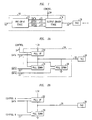
- Output buffer 10 includes a pre-drive stage 12 and an output driver stage 14.
- the pre-drive stage 12 includes an input terminal 16, for example, a plurality of input terminals receiving signals from other previous integrated circuit stages.
- the pre-drive stage 12 is coupled to the output driver stage 14 via a plurality of direct connections.
- the connections are labeled, for example, as a data terminal 21, a first data 1 terminal 22 and a second data 2 terminal 23.
- the first data 1 terminal 22 and the second data 2 terminal 23 represent the inverse of the data terminal 21, however, it is possible for one or both of them to be independent of the data terminal 21.
- the output driver stage 14 includes one or more control bit terminals or control bit input terminals 24, for example, for providing digital control bit information that enables pertinent portions of the output driver stage 14 to respond to the information on the data terminals 21-23.
- the digital control bit information is generated, for example, from a reference circuit that compares all or a portion of the output driver stage 14 to a discrete reference resistance value.
- the output driver stage 14 includes an output terminal 26, for example, a PAD 28 or other suitable terminal area.
- the PAD 28 typically is used for providing the connection between the output driver stage 14 and, for example, a transmission line (not shown) or the wiring interconnects between packaged devices (not shown), which could be modeled as a transmission line.
- FIG. 2a a schematic diagram of the output driver stage 14 of the integrated circuit (IC) output buffer 10 according to embodiments of the invention is shown.
- the output driver stage 14 includes pull-up and pull-down resistor arrangements.
- FIG. 2a shown in FIG. 2a is a pull-up resistor arrangement 52, a first pull-down resistor arrangement 54, and a second pull-down resistor arrangement 56.
- the pull-up resistor arrangement 52 has connected thereto the data terminal 21 and one or more control bit input terminals 24 of the output driver stage 14.
- control bit input terminals 24 are shown originating from a single source, it is possible for the control bit input terminals to originate from separate (different) sources. See, for example, FIG. 2b.
- the pull-up resistor arrangement 52 is connected to a supply voltage, for example, approximately 1.5 volts, and is connected to the PAD output terminal 26.
- the first pull-down resistor arrangement 54 has connected thereto the first data 1 terminal 22 and the control bits input terminal 24 of the output driver stage 14. As mentioned previously herein, although the control bit input terminals 24 are shown originating from a single source, it is possible for the control bit input terminals to originate from separate sources. Also, the first pull-down resistor arrangement 54 is connected to the ground voltage potential of the integrated circuit and, like the pull-up resistor arrangement 52, is connected to the PAD output terminal 26.
- the second pull-down resistor arrangement 56 has connected thereto the second data 2 terminal 23 and the control bits input terminal 24 of the output driver stage 14. Also, the second pull-down resistor arrangement 56 is connected to the ground voltage potential of the integrated circuit and, like the pull-up resistor arrangement 52 and the first pull-down resistor arrangement 54, is connected to the PAD output terminal 26.
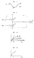
- a typically output driver output waveform is shown, for example, in FIG. 3.
- the value of the output driver output waveform varies, for example, from approximately 1.5 volts (shown generally as 62) to approximately 0.75 volts (shown generally as 64), depending on the desired output voltage state.
- the pull-up resistor arrangement 52 has a single transistor therein, for example, a single N-channel transistor device 66.
- the pull-down resistor arrangement 54 has a single transistor therein, for example, a single N-channel transistor device 68.
- the gate of transistor device 66 is connected to, for example, the data terminal 21 and the gate of the transistor device 68 is connected to a data terminal, which is, for example, the first data 1 terminal 22 or the second data 2 terminal 23.
- the digital control inputs are connected directly with the inventive pull-up and pull-down resistor arrangements to improve the linearity of the output buffer performance across the operating voltage range of the output driver (for example, 1.50 to 0.75 volts).
- the digital control bit information is generated, for example, from a reference circuit that compares a pull-up and/or pull-down resistor arrangement to a discrete reference resistance value.
- the digital control information control is varied in such a way that the voltage drop across the arrangements is the same as the voltage drop across the PAD 28 and its reference resistor (not shown). In this manner, the linearity of the output buffer is independent of external factors such as variations in ambient temperature, operating voltage and processing variations (that is, PVT variations).
- inventive pull-up and pull-down resistor arrangements are provided, including the pull-up resistor arrangements 70 shown in FIGs. 6-7 and the pull-down resistor arrangement shown in FIG. 8.
- the inventive pull-up and pull-down resistor arrangements include a plurality of (transistor) branches or legs connected in parallel.
- the number of branches within a particular arrangement varies, but should include as many branches as possible.
- the number of branches in a particular arrangement should give consideration to the corresponding increase in integrated circuit area that is required for the arrangement.
- Resistor arrangements according to embodiments of the invention typically have approximately ten (10) branches but can have as few as four (4) branches.
- the pull-up resistor arrangement 70 according to an embodiment of the invention is shown having, for example, eleven (11) branches connected in parallel between the supply voltage rail 75 and the output rail 77. More specifically, the pull-up resistor arrangement 70 is shown having seven (7) coarse tuning branches, three (3) fine tuning branches, and one (1) single fixed resistance branch. Also, alternatively, a diode 79 is connected between a source voltage, V DD , and the output rail 77 for protection from electrostatic discharge (ESD).
- ESD electrostatic discharge
- a single branch includes, for example, a first control transistor 74 (for example. a N-channel device), a second data transistor 76, and a resistor 78 connected as shown.
- a first control transistor 74 for example. a N-channel device
- a second data transistor 76 for example. a N-channel device
- a resistor 78 connected as shown.
- an additional resistor 72 is connected between the first control transistor 74 and the supply voltage rail 75 and the drain of the first control transistor 74.
- the gate of the first control transistor 74 is a control bit terminal, for example, one of the seven coarse control bit terminals (c 0 , c 1 , c 2 , c 3 , c 4 , c 5 , c 6 ) or one of the three fine control bit terminals (f 0 , f 1 , f 2 ).
- the gate of the first control transistor 74 in the single fixed resistance branch is connected to, for example, source voltage V DD .
- the source of the first control transistor 74 is connected to the drain of the second data transistor 76, which, for example, also is a N-channel device. Connected to the gate of the second data transistor 76 is the data terminal 21. The source of the second data transistor 76 is connected to the second resistor 78, which is connected as shown between the second data transistor 76 and an output rail 77 that is connectable with, for example, the PAD 28, which is external to the output driver stage 14.
- a branch is enabled when both the control bit (that is, the control bit terminal) and the data bit (that is, the data bit terminal) are both set to a logic high ("1"), for example, V DD .
- the data terminal 21 is set to a logical low (“0"), for example, V SS .
- the control bit terminals enable a branch depending on the logical value of the data terminal 21. If all the control bits are set to logical low and the data terminal 21 is set to logical high, the only enabled path will be the single fixed resistance branch, which remains enabled by virtue of its connection to V DD . If all the control bits are set to logical high and the data terminal 21 is set to logical low, all branches are enabled.
- the table set forth below characterizes the behavior of the control bits as a function of pressure, voltage and temperature (PVT) for a conventional 0.35 ⁇ m process.
- the line “fhl” refers to an arrangement whose operating speed is fast, whose power supply voltage is 1.5 volts and 3.3. volts, and whose operating temperature 0 °Celsius.
- the fastest device is characterized as "fhl”.
- two of the coarse branches are enabled (c 5 and c 6 ).
- the slowest device is characterized as "slh", where five coarse branches are enabled (c 2 , c 3 , c 4 , c 5 , c 6 ) and two fine branches (f 1 and f 2 ) are enabled.
- the values of the components used have been selected so that the full range of the branches is not used, for example, to allow for future flexibility and robustness (that is, extended temperature and voltage supply ranges).
- the value of the resistors and transistors in the branches is such that four fine bits have the same effect on the overall resistance of the output buffer as one coarse bit.
- FIG. 7a an alternative arrangement for a single pull-up (or pull-down) branch is shown.
- a single control and data (N-channel) transistor 80 is connected between first resistor 72 and second resistor 78 to perform the ANDing function performed by two transistors (control transistor 74 and data transistor 76) in the branches of the arrangement shown in FIG. 6.
- the control bit input terminal 24 and the data terminal 21 are operably connected to the transistor 80 through, for example, a NAND gate 82 and an inverter 84.
- FIG. 7a also is useful with a p-channel device.
- a single control and data (P-channel) transistor 85 is connected between first resistor 72 and second resistor 78 to perform the ANDing function.
- the control bit input terminal 24 and the data terminal 21 are operably connected to the transistor 85 through, for example, a NOR gate 87 and inverter 84.
- both control signal input terminal and data input terminal are used to enable transistor 80.
- the operation of the branch arrangements shown in FIGs. 7a-b differs from the branch arrangement shown in FIG. 6 in that the control signals and the data signals are combined logically and then applied to a single transistor.
- a pull-down arrangement 90 includes a plurality of branches connected in parallel.
- the branches include, for example, a third resistor 92, a third data transistor 94 and a fourth control transistor 96, for example, connected as shown.
- the third resistor 92 is operably connected to an output rail 98 connectable to, for example, the PAD 28.
- the third resistor 92 is operably connected to the drain of the third data transistor 94, which, for example, is a N-channel device.
- a data terminal Connected to the gate of the third data transistor 94 is a data terminal, for example, either the data 1 terminal or the data 2 terminal, depending on whether the pull-down arrangement is the first pull-down resistor arrangement 54 or the second pull-down resistor arrangement 56 (see, for example, FIG. 3).
- the source of the third data transistor 94 is connected to the drain of the fourth control transistor 96, which, for example, also is a N-channel device. Connected to the gate of the fourth control transistor 96 is a control bit terminal 24. The source of the fourth control transistor 96 is connected to the ground voltage potential of the integrated circuit.
- the branches are similar in form.
- the size of the resistors and the transistors vary.
- the resistors are sized for their respective resistance to be relatively large compared to the maximum resistance of the corresponding transistor(s).
- the operable range of linearity of the device and the single fixed resistance value of the range depends on the sizing of the resistors and transistors within the arrangement branches. In this manner, the number of branches and the values of the devices within the respective branch also affects the degree of tuning (that is, coarse and/or fine tuning) of the operable range of the device, as well as the range minimum.
- the seven (7) coarse tuning branches contain transistors with a width of 40 ⁇ m and are controlled by the coarse control bits (c 0 , c 1 , c 2 , c 3 , c 4 , c 5 , c 6 ).
- the three (3) fine tuning branches contain transistors with a width of 10 ⁇ m, or approximately one fourth the width of the coarse tuning branch transistors.
- the fine tuning branch transistors are controlled by fine control bits (f 0 , f 1 , f 2 ).
- the single fixed resistance branch which is provided to establishes a fixed base-point resistance value for the operable range, has a transistor with a width of 160 ⁇ m that is permanently enabled via its connection to V DD .
- the resistors in the coarse tuning branches each have a resistance size of approximately eight (8) squares, which translates to a resistance of approximately 200 ohms each.
- the resistors in the fine tuning branches each have a resistance size of approximately twenty-four (24) squares each, which translates to a resistance of approximately 800 ohms each.
- the resistors in the single fixed resistance branch each have a resistance size of approximately 1.7 squares, which translates to a resistance of approximately 43 ohms each.
- inventive resistor arrangements disclosed herein are useful alone or with other inventive resistor arrangements.
- inventive pull-up resistor arrangement 70 shown in FIG. 6 is useful with a conventional pull-down resistor arrangement or with an inventive pull-down resistor arrangement such as the pull-down resistor arrangement 90 shown in FIG. 8.
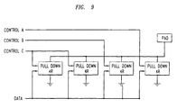
- FIG. 9 a plurality of pull-down arrangements each having, for example, a resistance of 4R, are connected in parallel as shown. Also, a plurality of enabling control input terminals are connected as shown.
- control input terminal A is set to a logical high (“1")
- the fourth pull-down arrangement is enabled and a resistance of 4R is provided.
- control input terminals A and B are set to a logical high (“1")
- the third and fourth pull-down arrangements are enabled and a resistance of 2R (4R in parallel with 4R) is provided.
- control input terminals A, B and C are set to a logical high (“1")
- the first, second third and fourth pull-down arrangements are enabled and a resistance of R (4R in parallel with 4R in parallel with 4R in parallel with 4R) is provided.
- a M-array signal is sent where the various signals are a different voltage signal.
Landscapes
- Engineering & Computer Science (AREA)
- Computer Hardware Design (AREA)
- Physics & Mathematics (AREA)
- Computing Systems (AREA)
- General Engineering & Computer Science (AREA)
- Mathematical Physics (AREA)
- Logic Circuits (AREA)
Applications Claiming Priority (2)
| Application Number | Priority Date | Filing Date | Title |
|---|---|---|---|
| US83172 | 1998-05-22 | ||
| US09/083,172 US6326821B1 (en) | 1998-05-22 | 1998-05-22 | Linearly-controlled resistive element apparatus |
Publications (1)
| Publication Number | Publication Date |
|---|---|
| EP0959564A1 true EP0959564A1 (fr) | 1999-11-24 |
Family
ID=22176640
Family Applications (1)
| Application Number | Title | Priority Date | Filing Date |
|---|---|---|---|
| EP19990303634 Withdrawn EP0959564A1 (fr) | 1998-05-22 | 1999-05-10 | Dispositif résistif à commande linéaire |
Country Status (3)
| Country | Link |
|---|---|
| US (1) | US6326821B1 (fr) |
| EP (1) | EP0959564A1 (fr) |
| JP (1) | JP3563295B2 (fr) |
Cited By (3)
| Publication number | Priority date | Publication date | Assignee | Title |
|---|---|---|---|---|
| WO2001076090A3 (fr) * | 2000-04-05 | 2002-04-11 | Conexant Systems Inc | Procede et appareil permettant de mettre en veille un etage d'attaque de ligne |
| GB2375446A (en) * | 2001-03-20 | 2002-11-13 | Hewlett Packard Co | Controlled impedance driver receiving a combination binary and thermometer code |
| CN100341246C (zh) * | 2003-02-18 | 2007-10-03 | 三星电子株式会社 | 开放漏极型输出缓冲器 |
Families Citing this family (23)
| Publication number | Priority date | Publication date | Assignee | Title |
|---|---|---|---|---|
| US6606705B1 (en) | 1999-09-15 | 2003-08-12 | Intel Corporation | Method and apparatus for configuring an I/O buffer having an initialized default signaling level to operate at a sampled external circuit signaling level |
| US6624662B1 (en) * | 2000-06-30 | 2003-09-23 | Intel Corporation | Buffer with compensating drive strength |
| US6864706B1 (en) * | 2000-07-20 | 2005-03-08 | Silicon Graphics, Inc. | GTL+Driver |
| FR2838888B1 (fr) * | 2002-04-22 | 2005-07-29 | St Microelectronics Sa | Procede de controle de l'impedance d'un dispositif semiconducteur d'amplification de sortie, et dispositif amplificateur de sortie correspondant |
| US6930506B2 (en) * | 2002-10-22 | 2005-08-16 | International Business Machines Corporation | Terminating resistor driver for high speed data communication |
| US6894529B1 (en) | 2003-07-09 | 2005-05-17 | Integrated Device Technology, Inc. | Impedance-matched output driver circuits having linear characteristics and enhanced coarse and fine tuning control |
| US6909305B1 (en) | 2003-08-08 | 2005-06-21 | Ami Semiconductor, Inc. | Digitally controlled impedance driver matching for wide voltage swings at input/output node and having programmable step size |
| KR100543197B1 (ko) * | 2003-08-25 | 2006-01-20 | 주식회사 하이닉스반도체 | 데이터 출력드라이버 |
| JP3949647B2 (ja) * | 2003-12-04 | 2007-07-25 | Necエレクトロニクス株式会社 | 半導体集積回路装置 |
| US6967501B1 (en) | 2003-12-18 | 2005-11-22 | Integrated Device Technology, Inc. | Impedance-matched output driver circuits having enhanced predriver control |
| JP4159553B2 (ja) | 2005-01-19 | 2008-10-01 | エルピーダメモリ株式会社 | 半導体装置の出力回路及びこれを備える半導体装置、並びに、出力回路の特性調整方法 |
| US7327167B2 (en) * | 2005-04-28 | 2008-02-05 | Silicon Graphics, Inc. | Anticipatory programmable interface pre-driver |
| US7586376B2 (en) * | 2005-12-01 | 2009-09-08 | Texas Instruments Incorporated | Pre-power amplifier of load, switch array, and impedance compensation |
| US7982499B2 (en) * | 2006-07-25 | 2011-07-19 | Atmel Corporation | Capacitive node isolation for electrostatic discharge circuit |
| JP4199789B2 (ja) * | 2006-08-29 | 2008-12-17 | エルピーダメモリ株式会社 | 半導体装置の出力回路調整方法 |
| KR100772533B1 (ko) * | 2006-09-27 | 2007-11-01 | 주식회사 하이닉스반도체 | 온 다이 터미네이션 회로 및 그의 구동 방법 |
| US7888968B2 (en) * | 2009-01-15 | 2011-02-15 | International Business Machines Corporation | Configurable pre-emphasis driver with selective constant and adjustable output impedance modes |
| US8436642B1 (en) * | 2011-08-23 | 2013-05-07 | Xilinx, Inc. | Control of termination capacitance for maximum transmitter bandwidth extension |
| US8847655B2 (en) * | 2012-05-22 | 2014-09-30 | Taiwan Semiconductor Manufacturing Company, Ltd. | Binary control arrangement and method of making and using the same |
| US9553587B2 (en) * | 2014-03-27 | 2017-01-24 | SK Hynix Inc. | Data output circuit of a semiconductor apparatus |
| KR102163263B1 (ko) * | 2014-03-27 | 2020-10-12 | 에스케이하이닉스 주식회사 | 반도체 장치의 데이터 출력 회로 |
| US9762237B1 (en) * | 2016-06-24 | 2017-09-12 | Qualcomm Incorporated | Constant impedance transmitter with variable output voltage limits |
| JP7102187B2 (ja) * | 2018-03-27 | 2022-07-19 | キヤノン株式会社 | カートリッジの製造方法 |
Citations (5)
| Publication number | Priority date | Publication date | Assignee | Title |
|---|---|---|---|---|
| EP0253914A1 (fr) * | 1986-07-23 | 1988-01-27 | Deutsche ITT Industries GmbH | Etage driver push-pull à transistors à effet de champ à porte isolée comportant une compensation de la fluctuation des paramètres de fonctionnement et de la dispersion de fabrication |
| US5220216A (en) * | 1992-01-02 | 1993-06-15 | Woo Ann K | Programmable driving power of a CMOS gate |
| US5589789A (en) * | 1993-10-16 | 1996-12-31 | Nec Corporation | Bus driver circuit for high-speed data transmission |
| EP0752677A2 (fr) * | 1995-07-07 | 1997-01-08 | Sun Microsystems, Inc. | Syntonisation paramétrique d'un circuit intégré après sa fabrication |
| US6127862A (en) * | 1997-09-01 | 2000-10-03 | Kabushiki Kaisha Toshiba | Programmable impedance circuit |
Family Cites Families (6)
| Publication number | Priority date | Publication date | Assignee | Title |
|---|---|---|---|---|
| US5001369A (en) * | 1990-07-02 | 1991-03-19 | Micron Technology, Inc. | Low noise output buffer circuit |
| JPH0469890A (ja) * | 1990-07-10 | 1992-03-05 | Nec Corp | 基準電圧発生回路 |
| US5243229A (en) | 1991-06-28 | 1993-09-07 | At&T Bell Laboratories | Digitally controlled element sizing |
| US5194765A (en) | 1991-06-28 | 1993-03-16 | At&T Bell Laboratories | Digitally controlled element sizing |
| US5621335A (en) | 1995-04-03 | 1997-04-15 | Texas Instruments Incorporated | Digitally controlled output buffer to incrementally match line impedance and maintain slew rate independent of capacitive output loading |
| US5917358A (en) * | 1997-12-09 | 1999-06-29 | Motorola, Inc. | Method and output buffer with programmable bias to accommodate multiple supply voltages |
-
1998
- 1998-05-22 US US09/083,172 patent/US6326821B1/en not_active Expired - Lifetime
-
1999
- 1999-05-10 EP EP19990303634 patent/EP0959564A1/fr not_active Withdrawn
- 1999-05-21 JP JP14089099A patent/JP3563295B2/ja not_active Expired - Fee Related
Patent Citations (5)
| Publication number | Priority date | Publication date | Assignee | Title |
|---|---|---|---|---|
| EP0253914A1 (fr) * | 1986-07-23 | 1988-01-27 | Deutsche ITT Industries GmbH | Etage driver push-pull à transistors à effet de champ à porte isolée comportant une compensation de la fluctuation des paramètres de fonctionnement et de la dispersion de fabrication |
| US5220216A (en) * | 1992-01-02 | 1993-06-15 | Woo Ann K | Programmable driving power of a CMOS gate |
| US5589789A (en) * | 1993-10-16 | 1996-12-31 | Nec Corporation | Bus driver circuit for high-speed data transmission |
| EP0752677A2 (fr) * | 1995-07-07 | 1997-01-08 | Sun Microsystems, Inc. | Syntonisation paramétrique d'un circuit intégré après sa fabrication |
| US6127862A (en) * | 1997-09-01 | 2000-10-03 | Kabushiki Kaisha Toshiba | Programmable impedance circuit |
Non-Patent Citations (1)
| Title |
|---|
| GABARA ET AL: "Digitally adjustable resistors in cmos for high-performance applications", IEEE JOURNAL OF SOLID-STATE CIRCUITS., vol. 27, no. 8, August 1992 (1992-08-01), IEEE INC. NEW YORK., US, pages 1176 - 1185, XP000309397, ISSN: 0018-9200 * |
Cited By (3)
| Publication number | Priority date | Publication date | Assignee | Title |
|---|---|---|---|---|
| WO2001076090A3 (fr) * | 2000-04-05 | 2002-04-11 | Conexant Systems Inc | Procede et appareil permettant de mettre en veille un etage d'attaque de ligne |
| GB2375446A (en) * | 2001-03-20 | 2002-11-13 | Hewlett Packard Co | Controlled impedance driver receiving a combination binary and thermometer code |
| CN100341246C (zh) * | 2003-02-18 | 2007-10-03 | 三星电子株式会社 | 开放漏极型输出缓冲器 |
Also Published As
| Publication number | Publication date |
|---|---|
| JP2000031811A (ja) | 2000-01-28 |
| US6326821B1 (en) | 2001-12-04 |
| JP3563295B2 (ja) | 2004-09-08 |
Similar Documents
| Publication | Publication Date | Title |
|---|---|---|
| US6326821B1 (en) | Linearly-controlled resistive element apparatus | |
| US6118310A (en) | Digitally controlled output driver and method for impedance matching | |
| US5214320A (en) | System and method for reducing ground bounce in integrated circuit output buffers | |
| US5231311A (en) | Digital output buffer and method with slew rate control and reduced crowbar current | |
| KR19990067849A (ko) | 허용 전압 출력 버퍼 | |
| US7633321B2 (en) | Driver circuit; electronic circuit having driver circuit and corresponding method | |
| EP0717527A2 (fr) | Ensemble d'attaque et de réception CMOS pour transmission bidirectionnelle simultanée | |
| US7863927B2 (en) | Semiconductor device | |
| US6300800B1 (en) | Integrated circuit I/O buffer with series P-channel and floating well | |
| JPH0334719A (ja) | 半導体集積回路 | |
| US6731164B2 (en) | Capacitor current multiplier capacitive feedback circuit | |
| US6184703B1 (en) | Method and circuit for reducing output ground and power bounce noise | |
| US6967501B1 (en) | Impedance-matched output driver circuits having enhanced predriver control | |
| US7154309B1 (en) | Dual-mode output driver configured for outputting a signal according to either a selected high voltage/low speed mode or a low voltage/high speed mode | |
| JP2000236244A (ja) | 広帯域で漏話を抑えた差動マルチプレクサ | |
| US6437611B1 (en) | MOS output driver circuit with linear I/V characteristics | |
| EP0347083B1 (fr) | Configuration de porte d'attaque de sortie TTL | |
| US20090027124A1 (en) | Level-Shifting Buffer | |
| US6362655B1 (en) | Linear active resistor and driver circuit incorporating the same | |
| JP3021145B2 (ja) | 電力供給バス上のノイズ制御の方法および装置 | |
| US11108396B2 (en) | Multivoltage high voltage IO in low voltage technology | |
| EP1454414B1 (fr) | Circuit de sortie a vitesse elevee pouvant fonctionner a basse tension | |
| US6268750B1 (en) | Flattened resistance response for an electrical output driver | |
| US20040246021A1 (en) | Modable dynamic terminator for high speed digital communications | |
| US7088130B2 (en) | Partial termination voltage current shunting |
Legal Events
| Date | Code | Title | Description |
|---|---|---|---|
| PUAI | Public reference made under article 153(3) epc to a published international application that has entered the european phase |
Free format text: ORIGINAL CODE: 0009012 |
|
| AK | Designated contracting states |
Kind code of ref document: A1 Designated state(s): DE FR GB |
|
| AX | Request for extension of the european patent |
Free format text: AL;LT;LV;MK;RO;SI |
|
| 17P | Request for examination filed |
Effective date: 20000511 |
|
| AKX | Designation fees paid |
Free format text: DE FR GB |
|
| 17Q | First examination report despatched |
Effective date: 20071115 |
|
| RAP3 | Party data changed (applicant data changed or rights of an application transferred) |
Owner name: LUCENT TECHNOLOGIES INC. |
|
| RAP1 | Party data changed (applicant data changed or rights of an application transferred) |
Owner name: ALCATEL-LUCENT USA INC. |
|
| RAP1 | Party data changed (applicant data changed or rights of an application transferred) |
Owner name: LUCENT TECHNOLOGIES INC. |
|
| STAA | Information on the status of an ep patent application or granted ep patent |
Free format text: STATUS: THE APPLICATION IS DEEMED TO BE WITHDRAWN |
|
| 18D | Application deemed to be withdrawn |
Effective date: 20150728 |