EP0960441B1 - Verfahren zur hermetischen abdichtung eines festkörperstrahlungsdetektors und nach diesem verfahren hergestellter detektor - Google Patents
Verfahren zur hermetischen abdichtung eines festkörperstrahlungsdetektors und nach diesem verfahren hergestellter detektor Download PDFInfo
- Publication number
- EP0960441B1 EP0960441B1 EP98903092A EP98903092A EP0960441B1 EP 0960441 B1 EP0960441 B1 EP 0960441B1 EP 98903092 A EP98903092 A EP 98903092A EP 98903092 A EP98903092 A EP 98903092A EP 0960441 B1 EP0960441 B1 EP 0960441B1
- Authority
- EP
- European Patent Office
- Prior art keywords
- layer
- detector
- scintillator
- slab
- deposition
- Prior art date
- Legal status (The legal status is an assumption and is not a legal conclusion. Google has not performed a legal analysis and makes no representation as to the accuracy of the status listed.)
- Expired - Lifetime
Links
Images

Classifications
-
- H—ELECTRICITY
- H10—SEMICONDUCTOR DEVICES; ELECTRIC SOLID-STATE DEVICES NOT OTHERWISE PROVIDED FOR
- H10F—INORGANIC SEMICONDUCTOR DEVICES SENSITIVE TO INFRARED RADIATION, LIGHT, ELECTROMAGNETIC RADIATION OF SHORTER WAVELENGTH OR CORPUSCULAR RADIATION
- H10F77/00—Constructional details of devices covered by this subclass
- H10F77/50—Encapsulations or containers
-
- H—ELECTRICITY
- H10—SEMICONDUCTOR DEVICES; ELECTRIC SOLID-STATE DEVICES NOT OTHERWISE PROVIDED FOR
- H10F—INORGANIC SEMICONDUCTOR DEVICES SENSITIVE TO INFRARED RADIATION, LIGHT, ELECTROMAGNETIC RADIATION OF SHORTER WAVELENGTH OR CORPUSCULAR RADIATION
- H10F39/00—Integrated devices, or assemblies of multiple devices, comprising at least one element covered by group H10F30/00, e.g. radiation detectors comprising photodiode arrays
- H10F39/10—Integrated devices
- H10F39/12—Image sensors
- H10F39/18—Complementary metal-oxide-semiconductor [CMOS] image sensors; Photodiode array image sensors
- H10F39/189—X-ray, gamma-ray or corpuscular radiation imagers
- H10F39/1898—Indirect radiation image sensors, e.g. using luminescent members
-
- H—ELECTRICITY
- H10—SEMICONDUCTOR DEVICES; ELECTRIC SOLID-STATE DEVICES NOT OTHERWISE PROVIDED FOR
- H10F—INORGANIC SEMICONDUCTOR DEVICES SENSITIVE TO INFRARED RADIATION, LIGHT, ELECTROMAGNETIC RADIATION OF SHORTER WAVELENGTH OR CORPUSCULAR RADIATION
- H10F39/00—Integrated devices, or assemblies of multiple devices, comprising at least one element covered by group H10F30/00, e.g. radiation detectors comprising photodiode arrays
- H10F39/80—Constructional details of image sensors
- H10F39/804—Containers or encapsulations
-
- H—ELECTRICITY
- H10—SEMICONDUCTOR DEVICES; ELECTRIC SOLID-STATE DEVICES NOT OTHERWISE PROVIDED FOR
- H10F—INORGANIC SEMICONDUCTOR DEVICES SENSITIVE TO INFRARED RADIATION, LIGHT, ELECTROMAGNETIC RADIATION OF SHORTER WAVELENGTH OR CORPUSCULAR RADIATION
- H10F39/00—Integrated devices, or assemblies of multiple devices, comprising at least one element covered by group H10F30/00, e.g. radiation detectors comprising photodiode arrays
- H10F39/80—Constructional details of image sensors
- H10F39/805—Coatings
- H10F39/8057—Optical shielding
Definitions
- the present invention relates to a method of waterproof sealing of a radiation detector, and more particularly a radiological matrix detector of large dimension consisting of a covered glass slab of amorphous silicon, the amorphous silicon constituting the active material of the elementary detectors of the matrix of detection.
- the invention applies to radiation detectors very short wavelengths, especially at X-rays used in radiology.
- the detectors of radiation are made from a matrix of elements photosensitive in solid state.
- Photosensitive elements in the solid state known are not directly sensitive to rays of very short wavelengths, for example X-rays. It is necessary to associate them with an organ scintillator. This is made of a substance that has the property, when excited by these X-rays, to emit light in a range of wavelengths larger: in the visible (or near visible). The precise wavelength depends on the substance used.
- the scintillator therefore acts as a length converter wave. The visible light thus generated is transmitted to photosensitive elements that convert photoelectric of the light energy received in signals electrics usable by electronic circuits appropriate.
- a scintillator according to known art is described, by way of nonlimiting example, in the patent application French FR-A-2 636 800 (THOMSON-CSF) and in US-A- 5434418.
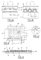
- Figures 1a to 1e illustrate the operation of a large-scale matrix radiation according to known art, formed by a glass slab covered with amorphous silicon. More specifically, Figure 1e shows an example of practical structure of such a detector. detector are typically one or more than ten centimeters aside, the detector can also be formed by several glass slabs that are knitted together when the dimensions are particularly large.
- Figures 1a and 1b show two sections lateral, orthogonal to each other, of a matrix of photosensitive elements conventionally associated with a sheet of scintillating substance.
- Each photosensitive element comprises a photodiode or a phototransistor, sensitive to photons, in the visible or near visible.
- each photosensitive element consists, for example, of two diodes, D mn1 and D mn2 , arranged head to tail and the matrix network RM comprises column conductors, Cc 1 to Cc x , and line conductors, Cl 1 to Cly.
- Each of the diodes, D mn1 and D mn2 constitutes in known manner, a capacitor when it is reverse biased.
- the first diode, D mn1 has a capacity typically ten times less than the capacity of the second diode, D mn2 . It mainly plays the role of switch, while the second diode is preferentially photodetector.
- D mn1 and D mn2 there is such a set of two head-to-tail diodes, D mn1 and D mn2 .
- the diodes, made of amorphous silicon can be replaced by transistors made in "TFT” technology, of the Anglo-Saxon “Thin Film Transistor” or “thin film transistor”, also based on amorphous silicon.
- the conductors 12 consist of a deposit of metal on an insulating substrate 10, preferably glass.
- the deposition is followed by a photogravure operation, in order to obtain parallel conductive tracks of appropriate width.
- the diodes (for example, D mn1 and D mn2 ) are formed by depositing, on the conductive tracks of columns 12, then etching, layers of amorphous silicon (Sia), intrinsic or doped using semiconductor materials of type P or N.
- a very thin layer of conductive material, preferably transparent, is deposited on the insulating layer 20, so as to form, after etching, the conductive tracks of lines 22 of the matrix network RM.
- the assembly described above forms what is generally called an "amorphous silicon slab".
- the substrate of the slab is in principle made of glass due to the low cost of this material.
- the row conductors, Cl 1 -Cl x , and the column conductors, Cc 1 -Cc y constitute the bias electrodes of the diode capacitors.
- the latter store electrical charges when they are subjected to light radiation and deliver an electrical signal, proportional to the stored charge, when they are electrically polarized.
- the addressing of the line conductors, Cl 1 -Cl x , and of the column conductors, Cc 1 -Cc y is carried out according to an appropriate chronology, so that all the pixels p mn are polarized sequentially in an order predetermined.
- the signal delivered by each pixel p mn is thus recovered and processed by electronic circuits (not shown), so as to reconstruct (point by point) the image stored in the form of electrical charges.
- connections to electronic circuits can be made using flexible multicore cables, 30 and 40, respectively.
- Multiconductive flexible cables have their ends fixed by gluing or welding or preferably by hot pressing on the peripheral connection zones. More specifically, they are usually produced by a flexing process, that is to say by hot pressing an anisotropic conductive film, hereinafter called "ACF", between contact pads located on the glass slab (substrate 10) and corresponding pads located on an external flexible cable 30.
- ACF anisotropic conductive film
- the conductive pads can be produced on the slab by vacuum deposition.
- the ACF has the particularity of having an electrical conduction after hot pressing, this only in the axis of the pressure exerted. Along the other axes, electrical isolation is preserved.
- the ACF After flexing, the ACF needs to be protected from external environment in order to maintain its properties adhesion and electrical conductivity, especially in difficult environmental conditions: humid heat, for example. More generally, whatever the method the nature of the flexible cable, the end of the flexible multicore cable must be protected in the area of connection.
- the photosensitive elements must be illuminated with visible light (or in a range close to visible light). It is necessary have a scintillator that converts x-rays into light energy in the visible spectrum. To do this, it just cover the amorphous silicon slab, previously described, with a layer of scintillating substance 24.
- CsI cesium iodide
- NaI sodium iodide
- TiI thallium
- the scintillator layer 24 is generally produced by vacuum evaporation. This last operation is usually followed by annealing the layer, which allows a homogeneous diffusion of the dopant at within the cesium iodide structure. Broadcasting as well obtained optimizes the conversion of X-rays to visible light.
- the most popular method of making a scintillator simple is to deposit a layer of cesium iodide on any substrate, to anneal it in order to obtain luminescence properties and report this set scintillator against the slab described above. More specifically, this reported scintillator can either be pressed against the slab, or optically coupled by bonding.
- the scintillator which is hygroscopic in nature, must be imperatively protected from the outside environment, so to preserve the luminescence properties. This protection can be achieved by isolating the scintillator from the external atmosphere by a tight seal in periphery of the scintillator substrate. We can fix the substrate on the slab by a bead of waterproof adhesive moisture. The substrate, by its impermeability, participates also to protect the scintillator.
- a more efficient method of carrying out scintillator, always in terms of resolution, consists of achieve this by direct evaporation of material on the slab.
- This solution has the advantage of obtaining a scintillator in intimate contact with the slab. Diffusion of light at the scintillator / slab interface and the loss of resulting resolutions are minimized.
- the scintillator protection can then be carried out as follows: on the layer, of scintillating substance 24, an entry window 26 to the X-rays.
- This window is made from a material such as aluminum, plastic or any other material suitable material transparent to X-rays. waterproof sealing as before. The entry window and the sealing bead also participate in this protection.
- Figure 1e illustrates, in section, the structure partial of a detector according to known art, of the type which has just been called back.
- the area protective material connection material and sealing bead material scintillator is not, a priori, of the same nature and compatible with each other, the two operations also being independent, the method according to known art requires define separate areas on the glass slab for two operations. This is therefore detrimental in terms space and increases the manufacturing time in multiplying the number of operations.
- the invention sets itself the goal, on the one hand, of overcoming the disadvantages of known art processes which have been recalled, and, on the other hand, to meet the needs that arise make you feel.
- the method according to the invention allows to provide simultaneous protection of the connectors and scintillator, protection obtained by the deposition of a material impermeable to atmospheric humidity.
- the deposit is done by screen printing.
- the subject of the invention is therefore a waterproof sealing method of a large matrix radiation formed by a glass slab covered with amorphous silicon, the slab comprising at least, on the one hand, a plurality of elementary detectors formed on an area central of an insulating substrate and, on the other hand, a layer of scintillating substance; said elementary detectors being connected to zones connector devices on which are fixed flexible multiconductor cables, said method comprising at least one step of depositing a layer of airtight material covering in a single operation both said areas connector peripherals and at least the periphery of said layer of scintillating substance.
- Figure 2 illustrates, in section, a first example for producing a detector according to the invention.
- the common elements with the detector of the figure carry it the same references and will only be re-described as of need.
- the scintillator 24 can be produced by evaporation direct.
- the member 26 is then a so-called "input" window, consisting of a sheet of moisture-proof material atmospheric (aluminum, plastic or glass, for example example).
- the scintillator 24 can also be attached on the slab, as described above.
- the organ 26 is then a substrate on which has been deposited the scintillating substance.
- protection of the peripheral connection area, on which are fixed the flexible cable ends multicore, and protecting the periphery of the scintillator 24 and its entry window 26 are produced in one operation.
- the deposit is preferably made by serigraphy. It can also be done using a mechanical dispensing machine, by any other method of filing or by a combination of the above methods.
- Figure 3 schematically illustrates, in section, a second embodiment of a detector according to the invention.
- the structure represented corresponds to the case where the scintillator 24 is produced by direct evaporation, as described above.
- the sealing is carried out by depositing a layer 7 of an airtight material over the entire surface of the scintillator 24.
- the layer 7 overflows on the periphery, towards the outside, of so as to also cover the connection area 3 and, in particular the bending zone 31. It is indeed necessary protect the entire surface of the scintillator 24, since it does not include any other means of protection.
- the method according to the invention therefore has many advantages and among these the following: simplicity, lower cost and reduced size.
Landscapes
- Measurement Of Radiation (AREA)
- Solid State Image Pick-Up Elements (AREA)
Claims (4)
- Verfahren zum dichten Versiegeln eines matrixförmigen Strahlungsdetektors großer Abmessungen, bestehend aus einer Glasplatte, die mit amorphem Silizium bedeckt ist und mindestens einerseits eine Vielzahl (RM) von Elementardetektoren (pmn), die auf einer zentralen Zone eines isolierenden Substrats (10) ausgebildet sind, und andrerseits eine Schicht (24) aus Szintillatorsubstanz enthält, wobei die Elementardetektoren (pmn) an randseitige Anschlußzonen (3) angeschlossen sind, in denen biegsame vieladrige Kabel befestigt sind, dadurch gekennzeichnet, daß es mindestens einen Schritt aufweist, bei dem eine Schicht (6, 7) aus einem gegen atmosphärische Feuchtigkeit dichten Material aufgebracht wird, die in einer einzigen Operation sowohl die randseitigen Anschlußzonen (3) als auch mindestens den Rand der Schicht (24) aus Szintillatorsubstanz bedeckt.
- Verfahren nach Anspruch 1, dadurch gekennzeichnet, daß die Schicht (24) aus Szintillatorsubstanz durch direktes Aufdampfen auf das die Vielzahl von Elementardetektoren (pmn) tragende Substrat (10) erfolgt und daß das Aufbringen der Schicht (7) aus einem gegen die atmosphärische Feuchtigkeit dichten Material so erfolgt, daß sie die Schicht (24) aus Szintillatorsubstanz vollständig bedeckt.
- Verfahren nach Anspruch 1 oder 2, dadurch gekennzeichnet, daß das Aufbringen der Schicht (6, 7) aus gegen die atmosphärische Feuchtigkeit dichtem Material durch Serigraphie erfolgt.
- Verfahren nach Anspruch 1 oder 2, dadurch gekennzeichnet, daß das Aufbringen der Schicht (6, 7) aus gegen die atmosphärische Feuchtigkeit dichtem Material mithilfe einer mechanischen Verteilmaschine aufgebracht wird.
Applications Claiming Priority (3)
| Application Number | Priority Date | Filing Date | Title |
|---|---|---|---|
| FR9700590A FR2758630B1 (fr) | 1997-01-21 | 1997-01-21 | Procede de scellement etanche d'un detecteur de rayonnement a l'etat solide et detecteur obtenu par ce procede |
| FR9700590 | 1997-01-21 | ||
| PCT/FR1998/000098 WO1998032179A1 (fr) | 1997-01-21 | 1998-01-20 | Procede de scellement etanche d'un detecteur de rayonnement et detecteur obtenu par ce procede |
Publications (2)
| Publication Number | Publication Date |
|---|---|
| EP0960441A1 EP0960441A1 (de) | 1999-12-01 |
| EP0960441B1 true EP0960441B1 (de) | 2003-04-02 |
Family
ID=9502817
Family Applications (1)
| Application Number | Title | Priority Date | Filing Date |
|---|---|---|---|
| EP98903092A Expired - Lifetime EP0960441B1 (de) | 1997-01-21 | 1998-01-20 | Verfahren zur hermetischen abdichtung eines festkörperstrahlungsdetektors und nach diesem verfahren hergestellter detektor |
Country Status (6)
| Country | Link |
|---|---|
| US (1) | US6354595B1 (de) |
| EP (1) | EP0960441B1 (de) |
| JP (1) | JP4388601B2 (de) |
| DE (1) | DE69812908D1 (de) |
| FR (1) | FR2758630B1 (de) |
| WO (1) | WO1998032179A1 (de) |
Families Citing this family (15)
| Publication number | Priority date | Publication date | Assignee | Title |
|---|---|---|---|---|
| US6146489A (en) * | 1998-11-19 | 2000-11-14 | General Electric Company | Method and apparatus for depositing scintillator material on radiation imager |
| EP1280207B1 (de) * | 2000-04-04 | 2017-03-15 | Hamamatsu Photonics K.K. | Halbleiter-energiedetektor |
| US6455855B1 (en) | 2000-04-20 | 2002-09-24 | Ge Medical Systems Global Technology Company Llc | Sealed detector for a medical imaging device and a method of manufacturing the same |
| EP1300694B1 (de) * | 2000-05-19 | 2011-03-23 | Hamamatsu Photonics K.K. | Strahlungsdetektor und verfahren zu seiner herstellung |
| US6414316B1 (en) * | 2000-11-30 | 2002-07-02 | Fyodor I. Maydanich | Protective cover and attachment method for moisture sensitive devices |
| JP4266898B2 (ja) * | 2004-08-10 | 2009-05-20 | キヤノン株式会社 | 放射線検出装置とその製造方法および放射線撮像システム |
| JP4926433B2 (ja) * | 2004-12-06 | 2012-05-09 | 株式会社Sokudo | 基板処理装置および基板処理方法 |
| JP4908947B2 (ja) | 2005-07-11 | 2012-04-04 | キヤノン株式会社 | 変換装置、放射線検出装置、及び放射線検出システム |
| JP5142943B2 (ja) * | 2007-11-05 | 2013-02-13 | キヤノン株式会社 | 放射線検出装置の製造方法、放射線検出装置及び放射線撮像システム |
| EP2344906A2 (de) * | 2008-10-07 | 2011-07-20 | Koninklijke Philips Electronics N.V. | Gehäuse für einen hygroskopischen szintillationskristall zur nuklearbildgebung |
| JP5562134B2 (ja) | 2010-06-17 | 2014-07-30 | キヤノン株式会社 | 放射線検出装置、その製造方法及び放射線撮像システム |
| JP5676397B2 (ja) * | 2010-11-09 | 2015-02-25 | 富士フイルム株式会社 | 放射線撮影装置 |
| US9281422B2 (en) * | 2011-03-24 | 2016-03-08 | Koninklijke Philips N.V. | Spectral imaging detector |
| US9448666B2 (en) * | 2013-06-08 | 2016-09-20 | Microsoft Technology Licensing, Llc | Dark film lamination for a touch sensor |
| CN107132186B (zh) * | 2017-06-28 | 2023-05-26 | 成都理工大学 | 海底沉积物探管及探测方法 |
Family Cites Families (17)
| Publication number | Priority date | Publication date | Assignee | Title |
|---|---|---|---|---|
| US4329701A (en) * | 1978-03-20 | 1982-05-11 | The Trane Company | Semiconductor package |
| US4543485A (en) * | 1981-11-24 | 1985-09-24 | Hitachi Chemical Company, Ltd. | Scintillator for radiation detection and process for producing the same |
| US5006714A (en) * | 1989-02-24 | 1991-04-09 | Radiation Measurements, Inc. | Scintillator dosimetry probe |
| US5227663A (en) * | 1989-12-19 | 1993-07-13 | Lsi Logic Corporation | Integral dam and heat sink for semiconductor device assembly |
| JP3216650B2 (ja) * | 1990-08-27 | 2001-10-09 | オリンパス光学工業株式会社 | 固体撮像装置 |
| FR2667981A1 (fr) * | 1990-10-12 | 1992-04-17 | Thomson Csf | Procede d'assemblage de deux couches constituees de materiaux differents et son application a l'encapsulation hermetique de circuits hybrides. |
| US5216278A (en) * | 1990-12-04 | 1993-06-01 | Motorola, Inc. | Semiconductor device having a pad array carrier package |
| US5179284A (en) * | 1991-08-21 | 1993-01-12 | General Electric Company | Solid state radiation imager having a reflective and protective coating |
| US5132539A (en) * | 1991-08-29 | 1992-07-21 | General Electric Company | Planar X-ray imager having a moisture-resistant sealing structure |
| US5434418A (en) * | 1992-10-16 | 1995-07-18 | Schick; David | Intra-oral sensor for computer aided radiography |
| US5557148A (en) * | 1993-03-30 | 1996-09-17 | Tribotech | Hermetically sealed semiconductor device |
| US5381014B1 (en) * | 1993-12-29 | 1997-06-10 | Du Pont | Large area x-ray imager and method of fabrication |
| EP0790652B1 (de) * | 1995-08-02 | 2007-02-21 | Matsushita Electric Industrial Co., Ltd. | Festkörperbildaufnahmegerät und herstellungsverfahren |
| JPH09260552A (ja) * | 1996-03-22 | 1997-10-03 | Nec Corp | 半導体チップの実装構造 |
| US5859475A (en) * | 1996-04-24 | 1999-01-12 | Amkor Technology, Inc. | Carrier strip and molded flex circuit ball grid array |
| JP2861956B2 (ja) * | 1996-07-24 | 1999-02-24 | 日本電気株式会社 | 高周波デバイスパッケージ及びその製造方法 |
| JPH11204679A (ja) * | 1998-01-08 | 1999-07-30 | Mitsubishi Electric Corp | 半導体装置 |
-
1997
- 1997-01-21 FR FR9700590A patent/FR2758630B1/fr not_active Expired - Fee Related
-
1998
- 1998-01-20 EP EP98903092A patent/EP0960441B1/de not_active Expired - Lifetime
- 1998-01-20 DE DE69812908T patent/DE69812908D1/de not_active Expired - Lifetime
- 1998-01-20 WO PCT/FR1998/000098 patent/WO1998032179A1/fr not_active Ceased
- 1998-01-20 JP JP53385898A patent/JP4388601B2/ja not_active Expired - Fee Related
- 1998-01-20 US US09/341,144 patent/US6354595B1/en not_active Expired - Lifetime
Also Published As
| Publication number | Publication date |
|---|---|
| US6354595B1 (en) | 2002-03-12 |
| FR2758630B1 (fr) | 1999-04-09 |
| FR2758630A1 (fr) | 1998-07-24 |
| WO1998032179A1 (fr) | 1998-07-23 |
| JP2001509317A (ja) | 2001-07-10 |
| JP4388601B2 (ja) | 2009-12-24 |
| EP0960441A1 (de) | 1999-12-01 |
| DE69812908D1 (de) | 2003-05-08 |
Similar Documents
| Publication | Publication Date | Title |
|---|---|---|
| EP0960441B1 (de) | Verfahren zur hermetischen abdichtung eines festkörperstrahlungsdetektors und nach diesem verfahren hergestellter detektor | |
| EP0316222B1 (de) | Röntgen-Bildaufnehmer | |
| EP0325525B1 (de) | Bildaufnahmevorrichtung mit kleiner Abmessung | |
| CA2339903C (fr) | Detecteur de rayonnement a l'etat solide a duree de vie accrue | |
| FR2834585A1 (fr) | Scellement de scintillateur ameliore pour un detecteur de rayons x a semiconducteurs | |
| FR2831671A1 (fr) | Detecteur de rayonnement x a l'etat solide | |
| EP0406053B1 (de) | Pyroelektrische Materialien enthaltende Infrarotfühler | |
| EP0316221A1 (de) | Matrix aus photoempfindlichen Elementen, die je aus einem Phototransistor und einem Speicherkondensator bestehen | |
| EP1927140A1 (de) | Herstellung eines strahlungssensors | |
| EP1573363B1 (de) | Festkörper-röntgenstrahlungsdetektor | |
| EP3066688B1 (de) | Digitaldetektor mit lichtgenerator zur aktivierung von optischem löschen | |
| EP1188187B1 (de) | Halbleiterdetektor für ionisierende strahlung | |
| EP0960442B1 (de) | Herstellungsverfahren eines strahlungsdetektors aus zusammengesetzten einzelelementen | |
| FR2758654A1 (fr) | Procede de realisation d'un detecteur de rayonnement a ecran plat et detecteur obtenu par ce procede | |
| FR2758655A1 (fr) | Procede de realisation d'un detecteur de radiographie par assemblage de dalles elementaires et detecteur ainsi obtenu | |
| EP4191675A1 (de) | Röntgenbildgebungsvorrichtung | |
| FR2849272A1 (fr) | Dispositif de detection photo-electrique et notamment de rayonnement x ou y | |
| WO2000075996A1 (fr) | Dispositif de detection de rayonnements connecte par film conducteur anisotrope | |
| EP0041647A1 (de) | Infrarotumsetzer | |
| FR2758679A1 (fr) | Procede de realisation d'un ecran matriciel par assemblage de dalles elementaires, ecran matriciel ainsi obtenu et son application a un detecteur de rayons x |
Legal Events
| Date | Code | Title | Description |
|---|---|---|---|
| PUAI | Public reference made under article 153(3) epc to a published international application that has entered the european phase |
Free format text: ORIGINAL CODE: 0009012 |
|
| 17P | Request for examination filed |
Effective date: 19990712 |
|
| AK | Designated contracting states |
Kind code of ref document: A1 Designated state(s): DE FR |
|
| GRAG | Despatch of communication of intention to grant |
Free format text: ORIGINAL CODE: EPIDOS AGRA |
|
| 17Q | First examination report despatched |
Effective date: 20020322 |
|
| GRAG | Despatch of communication of intention to grant |
Free format text: ORIGINAL CODE: EPIDOS AGRA |
|
| GRAH | Despatch of communication of intention to grant a patent |
Free format text: ORIGINAL CODE: EPIDOS IGRA |
|
| GRAH | Despatch of communication of intention to grant a patent |
Free format text: ORIGINAL CODE: EPIDOS IGRA |
|
| RAP1 | Party data changed (applicant data changed or rights of an application transferred) |
Owner name: THALES ELECTRON DEVICES S.A. |
|
| GRAA | (expected) grant |
Free format text: ORIGINAL CODE: 0009210 |
|
| AK | Designated contracting states |
Designated state(s): DE FR |
|
| REF | Corresponds to: |
Ref document number: 69812908 Country of ref document: DE Date of ref document: 20030508 Kind code of ref document: P |
|
| PG25 | Lapsed in a contracting state [announced via postgrant information from national office to epo] |
Ref country code: DE Free format text: LAPSE BECAUSE OF FAILURE TO SUBMIT A TRANSLATION OF THE DESCRIPTION OR TO PAY THE FEE WITHIN THE PRESCRIBED TIME-LIMIT Effective date: 20030703 |
|
| PLBE | No opposition filed within time limit |
Free format text: ORIGINAL CODE: 0009261 |
|
| STAA | Information on the status of an ep patent application or granted ep patent |
Free format text: STATUS: NO OPPOSITION FILED WITHIN TIME LIMIT |
|
| 26N | No opposition filed |
Effective date: 20040105 |
|
| PG25 | Lapsed in a contracting state [announced via postgrant information from national office to epo] |
Ref country code: FR Free format text: LAPSE BECAUSE OF NON-PAYMENT OF DUE FEES Effective date: 20040930 |
|
| REG | Reference to a national code |
Ref country code: FR Ref legal event code: ST |