EP0960725B1 - Mit Harz beschichtete Verbundfolie, ihre Herstellung und Verwendung - Google Patents
Mit Harz beschichtete Verbundfolie, ihre Herstellung und Verwendung Download PDFInfo
- Publication number
- EP0960725B1 EP0960725B1 EP19990110399 EP99110399A EP0960725B1 EP 0960725 B1 EP0960725 B1 EP 0960725B1 EP 19990110399 EP19990110399 EP 19990110399 EP 99110399 A EP99110399 A EP 99110399A EP 0960725 B1 EP0960725 B1 EP 0960725B1
- Authority
- EP
- European Patent Office
- Prior art keywords
- resin
- coated composite
- foil
- layer
- composite foil
- Prior art date
- Legal status (The legal status is an assumption and is not a legal conclusion. Google has not performed a legal analysis and makes no representation as to the accuracy of the status listed.)
- Expired - Lifetime
Links
Images
Classifications
-
- A—HUMAN NECESSITIES
- A63—SPORTS; GAMES; AMUSEMENTS
- A63B—APPARATUS FOR PHYSICAL TRAINING, GYMNASTICS, SWIMMING, CLIMBING, OR FENCING; BALL GAMES; TRAINING EQUIPMENT
- A63B53/00—Golf clubs
- A63B53/04—Heads
- A63B53/06—Heads adjustable
- A63B53/065—Heads adjustable for putters
-
- B—PERFORMING OPERATIONS; TRANSPORTING
- B32—LAYERED PRODUCTS
- B32B—LAYERED PRODUCTS, i.e. PRODUCTS BUILT-UP OF STRATA OF FLAT OR NON-FLAT, e.g. CELLULAR OR HONEYCOMB, FORM
- B32B15/00—Layered products comprising a layer of metal
- B32B15/04—Layered products comprising a layer of metal comprising metal as the main or only constituent of a layer, which is next to another layer of the same or of a different material
- B32B15/08—Layered products comprising a layer of metal comprising metal as the main or only constituent of a layer, which is next to another layer of the same or of a different material of synthetic resin
- B32B15/092—Layered products comprising a layer of metal comprising metal as the main or only constituent of a layer, which is next to another layer of the same or of a different material of synthetic resin comprising epoxy resins
-
- A—HUMAN NECESSITIES
- A63—SPORTS; GAMES; AMUSEMENTS
- A63B—APPARATUS FOR PHYSICAL TRAINING, GYMNASTICS, SWIMMING, CLIMBING, OR FENCING; BALL GAMES; TRAINING EQUIPMENT
- A63B53/00—Golf clubs
- A63B53/007—Putters
-
- A—HUMAN NECESSITIES
- A63—SPORTS; GAMES; AMUSEMENTS
- A63B—APPARATUS FOR PHYSICAL TRAINING, GYMNASTICS, SWIMMING, CLIMBING, OR FENCING; BALL GAMES; TRAINING EQUIPMENT
- A63B60/00—Details or accessories of golf clubs, bats, rackets or the like
- A63B60/02—Ballast means for adjusting the centre of mass
-
- A—HUMAN NECESSITIES
- A63—SPORTS; GAMES; AMUSEMENTS
- A63B—APPARATUS FOR PHYSICAL TRAINING, GYMNASTICS, SWIMMING, CLIMBING, OR FENCING; BALL GAMES; TRAINING EQUIPMENT
- A63B69/00—Training appliances or apparatus for special sports
- A63B69/36—Training appliances or apparatus for special sports for golf
- A63B69/3676—Training appliances or apparatus for special sports for golf for putting
- A63B69/3685—Putters or attachments on putters, e.g. for measuring, aligning
-
- B—PERFORMING OPERATIONS; TRANSPORTING
- B32—LAYERED PRODUCTS
- B32B—LAYERED PRODUCTS, i.e. PRODUCTS BUILT-UP OF STRATA OF FLAT OR NON-FLAT, e.g. CELLULAR OR HONEYCOMB, FORM
- B32B15/00—Layered products comprising a layer of metal
- B32B15/20—Layered products comprising a layer of metal comprising aluminium or copper
-
- B—PERFORMING OPERATIONS; TRANSPORTING
- B32—LAYERED PRODUCTS
- B32B—LAYERED PRODUCTS, i.e. PRODUCTS BUILT-UP OF STRATA OF FLAT OR NON-FLAT, e.g. CELLULAR OR HONEYCOMB, FORM
- B32B27/00—Layered products comprising a layer of synthetic resin
- B32B27/18—Layered products comprising a layer of synthetic resin characterised by the use of special additives
- B32B27/26—Layered products comprising a layer of synthetic resin characterised by the use of special additives using curing agents
-
- B—PERFORMING OPERATIONS; TRANSPORTING
- B32—LAYERED PRODUCTS
- B32B—LAYERED PRODUCTS, i.e. PRODUCTS BUILT-UP OF STRATA OF FLAT OR NON-FLAT, e.g. CELLULAR OR HONEYCOMB, FORM
- B32B27/00—Layered products comprising a layer of synthetic resin
- B32B27/28—Layered products comprising a layer of synthetic resin comprising synthetic resins not wholly covered by any one of the sub-groups B32B27/30 - B32B27/42
- B32B27/285—Layered products comprising a layer of synthetic resin comprising synthetic resins not wholly covered by any one of the sub-groups B32B27/30 - B32B27/42 comprising polyethers
-
- B—PERFORMING OPERATIONS; TRANSPORTING
- B32—LAYERED PRODUCTS
- B32B—LAYERED PRODUCTS, i.e. PRODUCTS BUILT-UP OF STRATA OF FLAT OR NON-FLAT, e.g. CELLULAR OR HONEYCOMB, FORM
- B32B27/00—Layered products comprising a layer of synthetic resin
- B32B27/28—Layered products comprising a layer of synthetic resin comprising synthetic resins not wholly covered by any one of the sub-groups B32B27/30 - B32B27/42
- B32B27/286—Layered products comprising a layer of synthetic resin comprising synthetic resins not wholly covered by any one of the sub-groups B32B27/30 - B32B27/42 comprising polysulphones; polysulfides
-
- B—PERFORMING OPERATIONS; TRANSPORTING
- B32—LAYERED PRODUCTS
- B32B—LAYERED PRODUCTS, i.e. PRODUCTS BUILT-UP OF STRATA OF FLAT OR NON-FLAT, e.g. CELLULAR OR HONEYCOMB, FORM
- B32B27/00—Layered products comprising a layer of synthetic resin
- B32B27/30—Layered products comprising a layer of synthetic resin comprising vinyl (co)polymers; comprising acrylic (co)polymers
- B32B27/306—Layered products comprising a layer of synthetic resin comprising vinyl (co)polymers; comprising acrylic (co)polymers comprising vinyl acetate or vinyl alcohol (co)polymers
-
- B—PERFORMING OPERATIONS; TRANSPORTING
- B32—LAYERED PRODUCTS
- B32B—LAYERED PRODUCTS, i.e. PRODUCTS BUILT-UP OF STRATA OF FLAT OR NON-FLAT, e.g. CELLULAR OR HONEYCOMB, FORM
- B32B27/00—Layered products comprising a layer of synthetic resin
- B32B27/38—Layered products comprising a layer of synthetic resin comprising epoxy resins
-
- B—PERFORMING OPERATIONS; TRANSPORTING
- B32—LAYERED PRODUCTS
- B32B—LAYERED PRODUCTS, i.e. PRODUCTS BUILT-UP OF STRATA OF FLAT OR NON-FLAT, e.g. CELLULAR OR HONEYCOMB, FORM
- B32B27/00—Layered products comprising a layer of synthetic resin
- B32B27/42—Layered products comprising a layer of synthetic resin comprising condensation resins of aldehydes, e.g. with phenols, ureas or melamines
-
- H—ELECTRICITY
- H05—ELECTRIC TECHNIQUES NOT OTHERWISE PROVIDED FOR
- H05K—PRINTED CIRCUITS; CASINGS OR CONSTRUCTIONAL DETAILS OF ELECTRIC APPARATUS; MANUFACTURE OF ASSEMBLAGES OF ELECTRICAL COMPONENTS
- H05K3/00—Apparatus or processes for manufacturing printed circuits
- H05K3/02—Apparatus or processes for manufacturing printed circuits in which the conductive material is applied to the surface of the insulating support and is thereafter removed from such areas of the surface which are not intended for current conducting or shielding
- H05K3/022—Processes for manufacturing precursors of printed circuits, i.e. copper-clad substrates
- H05K3/025—Processes for manufacturing precursors of printed circuits, i.e. copper-clad substrates by transfer of thin metal foil formed on a temporary carrier, e.g. peel-apart copper
-
- A—HUMAN NECESSITIES
- A63—SPORTS; GAMES; AMUSEMENTS
- A63B—APPARATUS FOR PHYSICAL TRAINING, GYMNASTICS, SWIMMING, CLIMBING, OR FENCING; BALL GAMES; TRAINING EQUIPMENT
- A63B2102/00—Application of clubs, bats, rackets or the like to the sporting activity ; particular sports involving the use of balls and clubs, bats, rackets, or the like
- A63B2102/32—Golf
-
- A—HUMAN NECESSITIES
- A63—SPORTS; GAMES; AMUSEMENTS
- A63B—APPARATUS FOR PHYSICAL TRAINING, GYMNASTICS, SWIMMING, CLIMBING, OR FENCING; BALL GAMES; TRAINING EQUIPMENT
- A63B2225/00—Miscellaneous features of sport apparatus, devices or equipment
- A63B2225/09—Adjustable dimensions
- A63B2225/093—Height
-
- B—PERFORMING OPERATIONS; TRANSPORTING
- B32—LAYERED PRODUCTS
- B32B—LAYERED PRODUCTS, i.e. PRODUCTS BUILT-UP OF STRATA OF FLAT OR NON-FLAT, e.g. CELLULAR OR HONEYCOMB, FORM
- B32B2311/00—Metals, their alloys or their compounds
- B32B2311/12—Copper
-
- B—PERFORMING OPERATIONS; TRANSPORTING
- B32—LAYERED PRODUCTS
- B32B—LAYERED PRODUCTS, i.e. PRODUCTS BUILT-UP OF STRATA OF FLAT OR NON-FLAT, e.g. CELLULAR OR HONEYCOMB, FORM
- B32B2363/00—Epoxy resins
-
- B—PERFORMING OPERATIONS; TRANSPORTING
- B32—LAYERED PRODUCTS
- B32B—LAYERED PRODUCTS, i.e. PRODUCTS BUILT-UP OF STRATA OF FLAT OR NON-FLAT, e.g. CELLULAR OR HONEYCOMB, FORM
- B32B2457/00—Electrical equipment
- B32B2457/08—PCBs, i.e. printed circuit boards
-
- H—ELECTRICITY
- H05—ELECTRIC TECHNIQUES NOT OTHERWISE PROVIDED FOR
- H05K—PRINTED CIRCUITS; CASINGS OR CONSTRUCTIONAL DETAILS OF ELECTRIC APPARATUS; MANUFACTURE OF ASSEMBLAGES OF ELECTRICAL COMPONENTS
- H05K2201/00—Indexing scheme relating to printed circuits covered by H05K1/00
- H05K2201/03—Conductive materials
- H05K2201/0332—Structure of the conductor
- H05K2201/0335—Layered conductors or foils
- H05K2201/0358—Resin coated copper [RCC]
-
- Y—GENERAL TAGGING OF NEW TECHNOLOGICAL DEVELOPMENTS; GENERAL TAGGING OF CROSS-SECTIONAL TECHNOLOGIES SPANNING OVER SEVERAL SECTIONS OF THE IPC; TECHNICAL SUBJECTS COVERED BY FORMER USPC CROSS-REFERENCE ART COLLECTIONS [XRACs] AND DIGESTS
- Y10—TECHNICAL SUBJECTS COVERED BY FORMER USPC
- Y10S—TECHNICAL SUBJECTS COVERED BY FORMER USPC CROSS-REFERENCE ART COLLECTIONS [XRACs] AND DIGESTS
- Y10S428/00—Stock material or miscellaneous articles
- Y10S428/901—Printed circuit
-
- Y—GENERAL TAGGING OF NEW TECHNOLOGICAL DEVELOPMENTS; GENERAL TAGGING OF CROSS-SECTIONAL TECHNOLOGIES SPANNING OVER SEVERAL SECTIONS OF THE IPC; TECHNICAL SUBJECTS COVERED BY FORMER USPC CROSS-REFERENCE ART COLLECTIONS [XRACs] AND DIGESTS
- Y10—TECHNICAL SUBJECTS COVERED BY FORMER USPC
- Y10T—TECHNICAL SUBJECTS COVERED BY FORMER US CLASSIFICATION
- Y10T428/00—Stock material or miscellaneous articles
- Y10T428/12—All metal or with adjacent metals
- Y10T428/12493—Composite; i.e., plural, adjacent, spatially distinct metal components [e.g., layers, joint, etc.]
- Y10T428/12771—Transition metal-base component
- Y10T428/12861—Group VIII or IB metal-base component
- Y10T428/12903—Cu-base component
-
- Y—GENERAL TAGGING OF NEW TECHNOLOGICAL DEVELOPMENTS; GENERAL TAGGING OF CROSS-SECTIONAL TECHNOLOGIES SPANNING OVER SEVERAL SECTIONS OF THE IPC; TECHNICAL SUBJECTS COVERED BY FORMER USPC CROSS-REFERENCE ART COLLECTIONS [XRACs] AND DIGESTS
- Y10—TECHNICAL SUBJECTS COVERED BY FORMER USPC
- Y10T—TECHNICAL SUBJECTS COVERED BY FORMER US CLASSIFICATION
- Y10T428/00—Stock material or miscellaneous articles
- Y10T428/28—Web or sheet containing structurally defined element or component and having an adhesive outermost layer
- Y10T428/2839—Web or sheet containing structurally defined element or component and having an adhesive outermost layer with release or antistick coating
-
- Y—GENERAL TAGGING OF NEW TECHNOLOGICAL DEVELOPMENTS; GENERAL TAGGING OF CROSS-SECTIONAL TECHNOLOGIES SPANNING OVER SEVERAL SECTIONS OF THE IPC; TECHNICAL SUBJECTS COVERED BY FORMER USPC CROSS-REFERENCE ART COLLECTIONS [XRACs] AND DIGESTS
- Y10—TECHNICAL SUBJECTS COVERED BY FORMER USPC
- Y10T—TECHNICAL SUBJECTS COVERED BY FORMER US CLASSIFICATION
- Y10T428/00—Stock material or miscellaneous articles
- Y10T428/31504—Composite [nonstructural laminate]
- Y10T428/31511—Of epoxy ether
- Y10T428/31529—Next to metal
Definitions
- the invention relates to a resin-coated composite foil and a process for its production.
- a resin-coated composite foil as it is mentioned in the preamble of the patent claim 1 is known from the EP-A-0 148 602 .
- the known resin-coated composite foil comprises a carrier film which can be metal, a release coating disposed on a surface of the carrier film, a copper layer disposed on the release coating and an adhesive layer and dielectric support disposed on the copper foil.
- Laminates for printed wiring board used in electronic materials are commonly produced by impregnating a glass cloth, a kraft paper, a glass nonwoven fabric or the like with a thermosetting resin such as a phenolic resin or an epoxy resin, semicuring the thermosetting resin to thereby obtain a prepreg and laminating one side or both sides of the prepreg with a copper foil.
- multilayer printed wiring boards are commonly produced by forming wirings on both sides of a copper-clad laminate to thereby obtain an inner core material and laminating both sides of the inner core material, through the medium of prepregs, to additional copper foils.
- Printed wiring boards are produced by laminating such a resin film or resin-coated composite foil onto a printed wiring board furnished with wirings (inner core material) and then forming wirings and via holes.
- the thus obtained laminates possess such heat resistance, electrical properties and chemical resistance that are satisfactory in practical use as printed wiring board.
- the current copper foil used in the resin-coated copper foil is generally an electrolytic copper foil having a thickness of 12 to 35 ⁇ m
- the use of a thinner copper foil is required when it is intended to provide more minute circuits wirings, i.e., having very small wiring - lines and spaces.
- resin-coated copper foils produced by applying a resin varnish to an ultra-thin copper foil having a thickness of 12 ⁇ m or less and heating and drying the same have various drawbacks.
- the copper foil it is very likely for the copper foil to be broken during the coating, heating or drying step, thereby rendering stable production difficult.
- Another problem is that the applied resin layer shrinks during the drying step to thereby increase the likelihood of deformation of the resin-coated copper foil, namely curling thereof, with the result that the handling of the resin-coated copper foil is very difficult.
- the resin composition for use in the resin-coated copper foil must be as proposed by the inventors ( Japanese Patent Application No. Hei 9-176565 ) in order to prevent cracking of the resin layer, thereby restricting the resin blend formulation.
- the ultra-thin copper foils and inner wirings are combined to construct a multilayer board, the ultra-thin copper foils are broken or wrinkled by the unevenness of a surface of the inner wirings.
- the method of interposing a thick copper foil or plastic film between a hot press plate and a resin-coated copper foil during the laminating step is known as a countermeasure to the above problems.
- the method of producing a resin-coated composite foil from an ultra-thin copper foil furnished with a supporting metal foil (carrier) has been proposed as described in Japanese Patent Application Publication (Unexamined) No. Hei 9-36550 .
- the etchable type having its support metal foil selectively removed with the use of a liquid chemical or the peelable type having it support metal foil mechanically stripped is used as the above ultra-thin copper foil furnished with the supporting metal foil.
- the above method of interposing the thick copper foil or plastic film between the press hot plate and the resin-coated copper foil during the laminating step has drawbacks in that the cost of copper foil and plastic film are incurred and that the working efficiency is deteriorated. Further, when a plastic film is interposed, the plastic film is charged with static electricity so that dust in the working environment is likely to deposit on the surface of the plastic film. Thus, the dust is transferred to a product to thereby bring about etching failure or other problems. Moreover, the conventional production of a resin-coated composite foil from an ultrathin copper foil furnished with the supporting metal foil has also drawbacks.
- the use of the etchable type carrier creates problems in that the number of process steps is increased by the etching and disposal of etching waste liquid is required.
- the use of the peelable type carrier creates problems in that it is difficult to optimize the bonding strength between the supporting metal foil and the ultra-thin copper foil. That is, when the bonding strength is too low, although the stripping of the supporting metal foil after lamination onto a base material is facilitated, peeling is likely to occur between the supporting metal foil and the ultra-thin copper foil when, while applying the organic insulation layer, heating and drying is carried out after the application of a resin varnish.
- a sodium hydroxide solution is used as a cleaning liquid for removing dust and other matter resulting from layer perforation.
- This sodium hydroxide solution corrodes the insulation resin, thereby the diameter of via holes formed in the insulation resin layer is larger than desired.
- a resin composition comprising an epoxy resin blend consisting of an epoxy resin and a curing agent therefor and a thermoplastic resin which is soluble in a solvent and has a functional group, other than an alcoholic hydroxyl group, polymerizable with epoxy resins is available as an alkali resistant resin.
- this resin composition has drawbacks in that, in the B-stage (semicured), cracking is likely to occur in the resin composition and that deformation of resin-coated copper foil during handling thereof is likely to crack the insulation resin layer.
- the inventors have made extensive and intensive studies with a view toward solving the above problems.
- the above technical problems and drawbacks of the prior art can be resolved by disposing an organic insulation layer on an ultra-thin copper foil provided on a supporting metal foil through an organic release layer.
- the present invention has been completed on the basis of this finding.
- An object of the present invention is to solve the above problems of the prior art.
- An object of the present invention is to provide a resin-coated composite foil which is free from the peeling of the supporting metal foil and the ultra-thin copper foil from each other even during the resin varnish coating and heating/drying steps and which permits extremely easy stripping of the supporting metal foil after the lamination onto a base material.
- a further object of the present invention is to provide a printed wiring board which has excellent workability in laser and plasma machining workability and can be made with fine wirings and via holes.
- Another object of the present invention is to provide processes for producing a multilayer copper-clad laminate and a multilayer printed wiring board with the use of the resin-coated composite foil having high alkali resistance.
- the resin-coated composite foil of the present invention is composed as it is mentioned in patent claim 1.
- the process for producing a resin-coated composite foil according to the present invention comprises the steps mentioned in claim 16.
- the process for producing a multilayer copper-clad laminate according to the present invention comprises the steps mentioned in claim 17 and embodiments thereof are defined in claims 18 to 19.
- the resin-coated composite foil of the present invention will be described in detail below.
- the resin-coated composite foil of the present invention comprises:
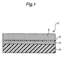
- Fig. 1 is a schematic sectional view showing one embodiment of the resin-coated composite foil of the present invention.
- an organic release layer 3 and an ultra-thin copper foil 4 are disposed in this order on a supporting metal layer 2. Further, an organic insulation layer 5 is disposed on the ultra-thin copper foil 4.
- the supporting metal layer 2 is preferably composed of copper or a copper alloy because the organic release layer 3 for use in the present invention forms a chemical bond with copper.
- the use of copper or a copper alloy is further advantageous in that the supporting metal layer after stripping can be recycled as a raw material for copper foil production.
- the supporting metal layer 2 can also be composed of a material other than the copper and copper alloy, for example, copper-plated aluminum.
- the thickness of the supporting metal layer 2 is not particularly limited, and the supporting metal layer 2 may be, for example, a foil having a thickness of 10 to 18 ⁇ m. When the supporting metal layer 2 is relatively thin, it may be referred to as a foil. However, the thickness of the supporting metal layer 2 may be larger than that of common foil, and use can be made of, for example, a thicker supporting sheet of about 5 mm or less thickness.
- the organic release layer 3 is composed of an organic compound selected from the group consisting of nitrogen-containing compounds, sulfur-containing compounds and carboxylic acids.
- the nitrogen-containing compounds are preferably nitrogen-containing compounds having a substituent (functional group).
- triazole compounds having a substituent (functional group) such as carboxybenzotriazole (CBTA), N',N'-bis(benzotriazolylmethyl)urea (BTD-U) and 3-amino-1H-1,2,4-triazole (ATA) are specially preferred.
- sulfur-containing compounds examples include mercaptobenzothiazole (MBT), thiocyanic acid (TCA) and 2-benzimidazolethiol (BIT).
- the carboxylic acids are, for example, high-molecular-weight carboxylic acids. Of these, monocarboxylic acids, for example, fatty acids derived from animal or plant fats and oils are preferred.
- the fatty acids may be saturated fatty acids or unsaturated fatty acids such as oleic acid, linolic acid and linolenic acid.
- the the organic release layer 3 composed of the above organic compounds prevents peeling of the supporting metal layer 2 and the ultra-thin copper foil 4 from each other and enables very easy stripping of the supporting metal layer 2 after the lamination onto a base material.
- the ultra-thin copper foil 4 for use in the resin-coated composite foil 1 of the present invention has a thickness of 12 ⁇ m or less, preferably 5 ⁇ m or less. when the copper foil has a thickness of greater than 12 ⁇ m, it can be handled without the aid of the supporting metal layer.
- the organic insulation layer 5 for use in the resin-coated composite foil 1 of the present invention can be composed of a material which is not particularly limited as long as it is an insulation resin commercially available for electrical and electronic uses. However, insulation resins which are excellent in alkali resistance are preferred because alkali solutions are used for cleaning via holes after laser perforation.
- An insulation resin composition comprising:
- a curing accelerator may be contained in the epoxy resin blend (i).
- the above insulation resin composition can be used in the form of a resin varnish by dissolving it in a solvent such as methyl ethyl ketone.
- the above insulation resin composition has a drawback of being readily cracked in the B-stage and, hence, it is difficult to use the resin composition for a resin layer of nonsupported resin-coated copper foil.
- the inventors have found that, when it is used as an organic insulation layer of supported composite foil, the deformation of copper foil during the handling thereof is reduced to thereby enable the use of the insulation resin composition.
- the epoxy resin for use in the epoxy resin blend is not particularly limited as long as it is of the type useful as electrical and electronic materials.
- suitable epoxy resins include bisphenol A epoxy resin, bisphenol F epoxy resin, novolak epoxy resin, cresol novolak epoxy resin, tetrabromobisphenol resin and glycidylamine epoxy resin.
- a curing agent which has low activity at room temperature but induces curing upon being heated namely a latent curing agent
- dicyandiamide, an imidazole, an aromatic amine, phenol novolak resin or cresol novolak resin is used as the latent curing agent.
- the epoxy resin blend (i) may contain a curing accelerator for accelerating the reaction between the epoxy resin and the curing agent therefor.
- a tertiary amine or an imidazole can be used as the curing accelerator.
- the epoxy resin blend (i) is mixed in an amount of 95 to 50 parts by weight, relative to 100 parts by weight of the total amount of the insulation resin composition for use in the present invention.
- the amount of mixed epoxy resin blend (i) in the insulation resin composition is less than 50 parts by weight, the adherence to a base material such as FR-4 may be decreased.
- the amount is greater than 95 parts by weight, it is very likely for the resin layer to break even when the resin-coated copper foil has a supporting metal layer in combination, thereby rendering the handleability thereof extremely poor.
- thermoplastic resin (ii) which is soluble in a solvent and has a functional group, other than an alcoholic hydroxyl group, polymerizable with the epoxy resin is preferably selected from the group consisting of polyvinylacetal resins, phenoxy resins and polyether sulf one resins. These thermoplastic resins may be used in combination.
- thermoplastic resin (ii) can be used in the form of a varnish by dissolving it in a solvent such as methyl ethyl ketone and combining the solution with the epoxy resin blend.
- the reactivity of the epoxy resin with an alcoholic hydroxyl group is so low that it is difficult to crosslink a thermoplastic resin having only an alcoholic hydroxyl group as a reactive functional group with the epoxy resin.
- mixing a thermoplastic resin having only an alcoholic hydroxyl group as a reactive functional group with the epoxy resin may invite lowering of water and heat resistances, so that the mixture thereof is not suitable to the use as a material for printed wiring board.
- the reactive functional group other than an alcoholic hydroxyl group there can be mentioned, for example, a phenolic hydroxyl group, a carboxyl group and an amino group.
- thermoplastic resin having any of these functional groups When use is made of the thermoplastic resin having any of these functional groups, the thermoplastic resin and the epoxy resin are easily crosslinked with each other at the time of curing to thereby enable avoiding the above problems (lowering of heat and water resistances). It is preferred to use 5 to 50 parts by weight of the thermoplastic resin having a functional group, other than an alcoholic hydroxyl group, polymerizable with the epoxy resin, relative to 100 parts by weight of the total amount of the insulation resin composition.
- the amount of the thermoplastic resin having a functional group, other than an alcoholic hydroxyl group, polymerizable with the epoxy resin is less than 5 parts by weight, the fluidity of the resin composition is so high that, unfavorably, the thickness of the insulation resin layer of a laminate after press forming is likely to become uneven.
- the degree of shrinkage of the insulation resin layer is so large at the time of cooling after drying that the deformation (curling) of the resin-coated composite foil is likely to occur whereby the supporting metal layer and the ultra-thin copper foil may be separated from each other.
- stable production may be hampered.
- This organic insulation layer may further contain other resin components such as a thermosetting polyimide resin, a urethane resin, a phenolic resin or a phenoxy resin within such an extent that the gist of the present invention is not departed from.
- resin components such as a thermosetting polyimide resin, a urethane resin, a phenolic resin or a phenoxy resin within such an extent that the gist of the present invention is not departed from.
- the addition of these resin components enables enhancing, for example, flame resistance and resin fluidity.
- This organic insulation layer is in the state of being partially cured, or semicured (B-stage) When the organic insulation layer is in the above state, the resin fluidity exhibited at the time of lamination and the easiness of embedding inner wiring therein can be controlled.
- the thickness of the organic insulation layer is not particularly limited, it is preferred that the organic insulation layer have a thickness of about 30 to 100 ⁇ m for ensuring the easy embedding of inner wirings and sufficient insulation.
- the process for producing a resin-coated composite foil according to the present invention comprises the steps of:
- an organic release layer is formed on a supporting metal layer.
- any oxide film formed on the surface of the supporting metal layer may be removed by acid washing and water washing.
- the organic release layer may be formed by the immersion method, the coating method or any other method capable of forming a uniform layer on a supporting member.
- the supporting metal layer is immersed in an aqueous solution of an organic compound such as a triazole so that the organic release layer is formed thereon.
- the concentration of aqueous solution is preferably in the range of 0.01 to 10 g/L, still preferably 0.1 to 10 g/L.
- the immersion time is preferably in the range of 5 to 60 sec.
- any excess adhering matter be washed away with water after the taking out of the supporting member from the solution so that only a very thin organic release layer remains on the surface of the supporting member. It is satisfactory if the thickness of the organic release layer after washing is generally in the range of 30 to 100 ⁇ , especially 30 to 60 ⁇ .
- an ultra-thin copper foil layer is formed on the thus formed organic release layer.
- the ultra-thin copper foil layer is electrodeposited on the organic release layer disposed on the supporting metal layer with the use of a plating bath.
- the electrodeposition of copper can be effected by the use of, for example, a copper pyrophosphate plating bath, an acidic copper sulfate plating bath or a copper cyanide plating bath. Although any of various electrodeposition baths can be applied, suitable electrodeposition bath can be selected in conformity with the particular objective.
- an adhesion promoting treatment may be applied to the outer surface of the ultra-thin copper foil by using known methods, for example, a roughening treatment (nodulation) in which a multitude of conductive fine particles are electrodeposited on the foil surface by regulating electrodeposition conditions.
- a roughening treatment in which a multitude of conductive fine particles are electrodeposited on the foil surface by regulating electrodeposition conditions.
- An example of the roughening treatment is disclosed in, for example, U.S. Patent No. 3,674,656 .
- the surface of the ultra-thin copper foil which may be subjected to the roughening treatment may be passivated for preventing the oxidation of the ultra-thin copper foil. The passivation may be carried out alone or may be preceded by roughening treatment.
- the passivation is generally effected by electrodepositing a member selected from the group consisting of zinc, zinc chromate, nickel, tin, cobalt and chromium on the surface of the ultra-thin copper foil.
- a member selected from the group consisting of zinc, zinc chromate, nickel, tin, cobalt and chromium on the surface of the ultra-thin copper foil.
- An example of passivation is disclosed in U.S. Patent No. 3,625,844 .
- an organic insulation layer is formed on the surface of the ultra-thin copper foil.
- the method of forming the organic insulation layer is not particularly limited.
- the organic insulation layer can be formed by application of a resin varnish obtained by combining the above epoxy resin blend (i) with a solution of the above thermoplastic resin (ii) in a dissolving solvent.
- the dissolving solvent is not particularly limited.
- methyl ethyl ketone is used as the dissolving solvent
- the proportion of added dissolving solvent to the thermoplastic resin (ii) is not particularly limited as long as the resultant resin varnish has a viscosity suitable for coating.
- the resin-coated composite foil can generally be obtained by carrying out heating and drying after the formation of the organic insulation layer.
- the heating and drying conditions are not particularly limited and can be determined depending on the resin formulation of employed insulation resin composition and the type of employed solvent, although heating at 130 to 200°C for 1 to 10 min is preferred from the viewpoint of productivity and solvent recovery efficiency.
- the organic insulation layer is in the state of being partially cured, namely semicured (B-stage), so that the resin fluidity and embedding of internal-layer wirings at lamination can be controlled.
- a multilayer copper-clad laminate can be produced by a process comprising the steps of:
- any resin base materials commonly used in electronic device applications can be employed as the insulation base layer without any particular limitation, which include, for example, FR-4 (glass fiber reinforced epoxy), paper/phenolic and paper/epoxy base materials.
- the lamination of the copper-clad laminate with the resin-coated composite foil is carried out by heating under pressure according to the press forming or roll lamination technique. As a result, the semicured organic insulation layer is fully cured.
- a multilayer printed wiring board can be produced by, after the stripping of the supporting metal layer to expose the ultra-thin copper foil on the surface of the multilayer copper-clad laminate, drilling the multilayer copper-clad laminate to thereby form through holes and irradiating the ultra-thin copper foil layer with laser, such as UV-YAG layer or carbon dioxide laser, or plasma to form via holes, followed by panel plating and etching to thereby form wirings.
- laser such as UV-YAG layer or carbon dioxide laser
- a printed wiring board with an increased number of layers can be produced by repeating these steps for producing the multilayer printed wiring board.
- the resin-coated composite foil of the present invention prevents the occurrence of blisters and peeling between the supporting metal layer and the ultra-thin copper foil during the production of the copper-clad laminate.
- the resin-coated composite foil is one including an ultra-thin copper foil, the handleability thereof is excellent.
- the copper-clad laminate produced from this resin-coated composite foil is excellent in laser workability and permits easily forming fine wirings.
- a printed wiring board permitting in the formation of fine wirings and the formation of via holes by laser or plasma can be made by using a composite foil with an ultra-thin copper foil and a specific resin composition.
- Electrolytic copper foil of 35 ⁇ m thickness was provided as a supporting metal layer.
- the electrolytic copper foil had a rough side (matte side) and a smooth side (shiny side).
- an organic release layer was formed and then was subjected to the following first copper plating, second copper plating, roughening treatment and passivation in sequence as follows.
- the electrolytic copper foil for use as a supporting metal layer was immersed in a 2 g/L carboxybenzotriazole (CBTA) solution heated at 30°C for 30 sec, taken out from the solution and washed with water. Thus, an organic release layer of CBTA was formed.
- CBTA carboxybenzotriazole
- a 1 ⁇ m thick layer of copper was deposited on the surface of the organic release layer formed on the shiny side surface of the electrolytic copper foil by performing a cathodic electrolysis in a pH 8.5 copper pyrophosphate bath containing 17 g/L of copper and 500 g/L of potassium pyrophosphate heated at 50°C, in which a current density was 3 A/dm 2
- the surface of the thus formed ultra-thin copper foil was washed with water, and a 2 ⁇ m thick layer of copper was deposited thereon by performing a cathodic electrolysis in a copper sulfate bath containing 80 g/L of copper and 150 g/L of sulfuric acid heated at 50°C, in which a current density was 60 A/dm 2 As a result, there was obtained an ultra-thin copper foil layer having a total thickness of 3 ⁇ m.
- the surface of the resultant ultra-thin copper foil layer was subjected to a conventional roughening treatment.
- the treated side surface of the ultra-thin copper foil layer was passivated with zinc chromate by the conventional method. Thus, a composite copper foil was obtained.
- the surface of ultra-thin copper foil of the thus obtained composite copper foil was coated with a 80 ⁇ m thick (in terms of solid contents) layer of the insulation resin composition of the following formulation and heated in an oven at 150°C for 4 min to thereby effect solvent removal and drying.
- the resin was semicured to thereby produce a resin-coated composite foil. No blister and peeling occurred between the supporting copper foil and the ultra-thin copper foil layer.
- Bisphenol A epoxy resin (trade name: Epomic R-140, produced by Mitsui Chemicals, Inc.) and o-cresol novolak epoxy resin (trade name: Epo Tohto YDCN-704, produced by Tohto Kasei K.K.) were mixed together in a weight ratio of 100 : 100.
- epoxy resin curing agent (trade name: Milex XL-225, produced by Mitsui Chemicals, Inc.) was added to the above epoxy resin mixture.
- epoxy resin curing accelerator (trade name: Curezol 2PZ, produced by Shikoku Chemicals Corporation) was added to the above epoxy resin mixture.
- Both sides of FR-4 copper-clad laminate (core thickness: 0.6 mm and copper foil thickness: 35 ⁇ m) having both sides furnished with wirings were each overlaid with the above obtained resin-coated composite foil so that the resin layer of the resin-coated composite foil contacted the FR-4 copper-clad laminate. Heating was performed at 175°C for 60 min under a pressure of 2 5 kgf /cm 2 so that the resin layer was cured.
- a multilayer printed wiring board was obtained by furnishing the multilayer copper-clad laminate with via holes and wirings in the manner comprising:
- the thus obtained multilayer printed wiring board was free from resin cracking at the time of layup.
- via holes could easily be formed therein by UV-YAG laser.
- the multilayer printed wiring board was also free from the dissolution of resin layer by the alkali cleaning liquid, enabled obtaining via holes with desired diameter and enabled forming wirings whose line width/line spacing was 60 ⁇ m/60 ⁇ m.
- support-bearing composite foils were produced. Specifically, three electrolytic copper foils each of 35 ⁇ m thickness were provided as supporting metal layers, and organic release layers were formed on the supporting electrolytic copper foils. 1 ⁇ m thick layers of copper were deposited on the organic release layers at the first copper plating. At the second copper plating, 4 ⁇ m thick, 8 ⁇ m thick and 11 ⁇ m thick copper layers were deposited thereon in Example 2, Example 3 and Example 4, respectively. Thus, ultra-thin copper foil layers of 5 ⁇ m, 9 ⁇ m and 12 ⁇ m total thicknesses were formed on the support-bearing composite foils in Example 2, Example 3 and Example 4, respectively.
- Resin-coated composite foils, multilayer copper-clad laminates and multilayer printed wiring boards were obtained from these three support-bearing composite foils having different thicknesses in the same manner as in Example 1.
- a resin-coated copper foil (resin layer thickness: 80 ⁇ m), multilayer copper-clad laminate and multilayer printed wiring board were produced in the same manner as in Example 1, except that use was made of a 7 ⁇ m thick electrolytic copper foil not furnished with any support copper foil, which had its rough side subjected to the same roughening treatment and passivation as in Example 1.
- the resin-coated copper foil was so extremely curled that the layup thereof was difficult, and suffered from cracking and resin peeling attributed to the curling.
Landscapes
- Engineering & Computer Science (AREA)
- Health & Medical Sciences (AREA)
- General Health & Medical Sciences (AREA)
- Physical Education & Sports Medicine (AREA)
- Manufacturing & Machinery (AREA)
- Microelectronics & Electronic Packaging (AREA)
- Life Sciences & Earth Sciences (AREA)
- Biophysics (AREA)
- Laminated Bodies (AREA)
- Production Of Multi-Layered Print Wiring Board (AREA)
Claims (19)
- Harzbeschichtete Verbundfolie (1), umfassend:eine Trägerschicht (2) aus Metall,eine organische Ablöseschicht (3), welche auf einer Oberfläche der Trägerschicht (2) aus Metall angeordnet ist,eine auf der organischen Ablöseschicht (3) angeordnete ultradünne Kupferfolie (4), undeine auf der ultradünnen Kupferfolie angeordnete organische Isolationsschicht (5), dadurch gekennzeichnet, dass die organische Ablöseschicht (3) eine Verbindung ausgewählt aus der Gruppe bestehend aus stickstoffhaltigen Verbindungen, schwefelhaltigen Verbindungen und Karbonsäuren umfasst.
- Harzbeschichtete Verbundfolie (1) gemäß Anspruch 1, bei der die organische Isolationsschicht (5) aus einer Harzverbindung gebildet ist, welche umfasst:(i) eine einen Epoxidharz und ein Härtungsmittel für diesen umfassende Epoxidharzmischung, und(ii) einen thermoplastischen Harz, der in einem Lösungsmittel löslich ist und eine funktionelle Gruppe mit Ausnahme einer alkoholartigen Hydroxylgruppe aufweist, und mit dem Epoxidharz polymerisierbar ist.
- Harzbeschichtete Verbundfolie (1) gemäß Anspruch 2, bei der der thermoplastische Harz aus einer Gruppe bestehend aus einem Polyvinylacetalharz, einem Phenoxyharz, und einem Polyethersulfonharz ausgewählt ist.
- Harzbeschichtete Verbundfolie (1) gemäß Anspruch 1, bei der die organische Ablöseschicht (3) eine stickstoffhaltige Verbindung umfasst.
- Harzbeschichtete Verbundfolie (1) gemäß Anspruch 4, bei der die organische Ablöseschicht (3) eine substituierte stickstoffhaltige Verbindung umfasst.
- Harzbeschichtete Verbundfolie (1) gemäß Anspruch 5, bei der die substituierte stickstoffhaltige Verbindung eine substitionierte Trialzolverbindung ist.
- Harzbeschichtete Verbundfolie (1) gemäß Anspruch 6, bei der die substituierte Triazolverbindung aus der Gruppe bestehend aus Carboxylbenzotriazol, N',N'bis(benzotriazolylmethyl) Harnstoff und 3-amino-1H-1,2,4-triazol ausgewählt ist.
- Harzbeschichtete Verbundfolie (1) gemäß Anspruch 1, bei der die organische Ablöseschicht (3) aus einer schwefelhaltigen Verbindung besteht.
- Harzbeschichtete Verbundfolie (1) gemäß Anspruch 8, bei der die schwefelhaltige Verbindung aus der Gruppe bestehend aus Mercaptobenzothiazol, Thiocyansäure und 2-benzimidazolethiol ausgewählt ist.
- Harzbeschichtete Verbundfolie (1) gemäß Anspruch 1, wobei die organische Ablöseschicht (3) eine Carbonsäure umfasst.
- Harzbeschichtete Verbundfolie (1) gemäß Anspruch 10, bei der die Carbonsäure eine Monocarbonsäure ist.
- Harzbeschichtete Verbundfolie (1) gemäß Anspruch 11, wobei die Monocarbonsäure aus der Gruppe bestehend aus Ölsäure, Linolsäure und Linolensäure ausgewählt ist.
- Harzbeschichtete Verbundfolie (1) gemäß Anspruch 1, wobei die ultradünne Kupferfolie (4) eine Dicke von 12 µm oder weniger aufweist.
- Harzbeschichtete Verbundfolie (1) gemäß Anspruch 13, wobei die ultradünne Kupferfolie (4) eine Dicke von 5 µm oder weniger aufweist.
- Harzbeschichtete Verbundfolie (1) gemäß Anspruch 1, wobei die Trägerschicht (2) aus Metall ein aus der Gruppe bestehend aus Kupfer, Kupferlegierungen und kupferbeschichtetem Aluminium ausgewähltes Metall umfasst.
- Verfahren zur Herstellung einer harzbeschichteten Verbundfolie (1) umfassend die Schritte:gleichförmiges Ausbilden einer organischen Ablöseschicht (3) auf einer Trägerschicht (2) aus Metall;galvanisches Abscheiden einer ultradünnen Kupferfolienschicht (4) auf der organischen Ablöseschicht (3); undAusbilden einer organischen Isolationsschicht (5) auf der ultradünnen Kupferfolienschicht, dadurch gekennzeichnet, dass die organische Ablöseschicht (3) eine Verbindung ausgewählt aus der Gruppe bestehend aus stickstoffhaltigen Verbindungen, schwefelhaltigen Verbindungen und Karbonsäuren umfasst.
- Verfahren zur Herstellung eines mehrlagigen, kupferplattierten Laminats, umfassend die Schritte:übereinanderschichten der harzbeschichteten Verbundfolie (A) gemäß Anspruch 1 undeines kupferplattierten Laminats (B) welches eine Isolationsbasisschicht umfasst, bei der eine Seite oder beide Seiten mit einer inneren Verdrahtung versehen sind;wobei die organische Isolationsschicht der harzbeschichteten Verbundfolie (A) die innere Verdrahtung des kupferplattierten Laminats (B) kontaktiert, und danach Hitze und Druck angewendet werden, um dadurch ein Laminat zu erhalten; und
Ablösen der Trägerschicht aus Metall von dem Laminat. - Verfahren zur Herstellung einer mehrlagigen Leiterplatte, umfassend ein Ausbilden einer äußeren Verdrahtung auf der ultradünnen Kupferfolienschicht des mittels des Verfahrens gemäß Anspruch 17 hergestellten mehrlagigen kupferplattierten Laminats.
- Verfahren gemäß Anspruch 18, wobei die äußere Verdrahtung durch die Schritte des Ausbildens von Durchgangslöchern unter der Verwendung eines UV-YAG Lasers oder Kohlenstoffdioxidlasers, der Flächengalvanisierung und des Ätzens ausgebildet wird.
Applications Claiming Priority (4)
| Application Number | Priority Date | Filing Date | Title |
|---|---|---|---|
| JP16619998 | 1998-05-29 | ||
| JP16619998 | 1998-05-29 | ||
| JP13699899 | 1999-05-18 | ||
| JP13699899A JP3612594B2 (ja) | 1998-05-29 | 1999-05-18 | 樹脂付複合箔およびその製造方法並びに該複合箔を用いた多層銅張り積層板および多層プリント配線板の製造方法 |
Publications (3)
| Publication Number | Publication Date |
|---|---|
| EP0960725A2 EP0960725A2 (de) | 1999-12-01 |
| EP0960725A3 EP0960725A3 (de) | 2002-08-14 |
| EP0960725B1 true EP0960725B1 (de) | 2008-03-12 |
Family
ID=26470437
Family Applications (1)
| Application Number | Title | Priority Date | Filing Date |
|---|---|---|---|
| EP19990110399 Expired - Lifetime EP0960725B1 (de) | 1998-05-29 | 1999-05-28 | Mit Harz beschichtete Verbundfolie, ihre Herstellung und Verwendung |
Country Status (9)
| Country | Link |
|---|---|
| US (1) | US6652962B1 (de) |
| EP (1) | EP0960725B1 (de) |
| JP (1) | JP3612594B2 (de) |
| KR (1) | KR100389468B1 (de) |
| CN (1) | CN1161228C (de) |
| DE (1) | DE69938322T2 (de) |
| MY (1) | MY129290A (de) |
| SG (1) | SG81285A1 (de) |
| TW (1) | TW436426B (de) |
Families Citing this family (63)
| Publication number | Priority date | Publication date | Assignee | Title |
|---|---|---|---|---|
| NL1014112C2 (nl) * | 2000-01-19 | 2001-07-20 | Corus Staal Bv | Metaal-kunststof-metaal laminaat en werkwijze voor het vervaardigen van een dergelijk laminaat. |
| US6871396B2 (en) | 2000-02-09 | 2005-03-29 | Matsushita Electric Industrial Co., Ltd. | Transfer material for wiring substrate |
| US6346335B1 (en) * | 2000-03-10 | 2002-02-12 | Olin Corporation | Copper foil composite including a release layer |
| EP1273682A4 (de) * | 2000-04-05 | 2003-04-16 | Nikko Materials Co Ltd | Kupferfolie mit durch laser erzeugtes loch |
| JP2002026475A (ja) * | 2000-07-07 | 2002-01-25 | Mitsui Mining & Smelting Co Ltd | キャリア箔付銅箔回路及びそれを用いたプリント配線板の製造方法並びにプリント配線板 |
| JP2002033581A (ja) * | 2000-07-13 | 2002-01-31 | Mitsui Mining & Smelting Co Ltd | 銅張積層板の製造方法 |
| JP3396465B2 (ja) * | 2000-08-25 | 2003-04-14 | 三井金属鉱業株式会社 | 銅張積層板 |
| US7026059B2 (en) * | 2000-09-22 | 2006-04-11 | Circuit Foil Japan Co., Ltd. | Copper foil for high-density ultrafine printed wiring boad |
| TWI295966B (de) * | 2000-10-27 | 2008-04-21 | Kaneka Corp | |
| JP2002292788A (ja) * | 2001-03-30 | 2002-10-09 | Nippon Denkai Kk | 複合銅箔及び該複合銅箔の製造方法 |
| KR100671541B1 (ko) * | 2001-06-21 | 2007-01-18 | (주)글로벌써키트 | 함침 인쇄회로기판 제조방법 |
| LU90804B1 (fr) * | 2001-07-18 | 2003-01-20 | Circuit Foil Luxembourg Trading Sarl | Process for manufacturing a composite foil suitable for manufacturing multi-layer printed circuit boards |
| JP4006618B2 (ja) | 2001-09-26 | 2007-11-14 | 日鉱金属株式会社 | キャリア付銅箔の製法及びキャリア付銅箔を使用したプリント基板 |
| JP2003101189A (ja) * | 2001-09-26 | 2003-04-04 | Japan Rec Co Ltd | キャリア付銅箔及び該銅箔を使用したプリント基板 |
| JP3973197B2 (ja) * | 2001-12-20 | 2007-09-12 | 三井金属鉱業株式会社 | キャリア箔付電解銅箔及びその製造方法 |
| JP4073248B2 (ja) | 2002-05-14 | 2008-04-09 | 三井金属鉱業株式会社 | 高温耐熱用キャリア箔付電解銅箔の製造方法及びその製造方法で得られる高温耐熱用キャリア箔付電解銅箔 |
| JP4178415B2 (ja) * | 2002-07-04 | 2008-11-12 | 三井金属鉱業株式会社 | キャリア箔付電解銅箔 |
| WO2004014114A1 (ja) * | 2002-07-31 | 2004-02-12 | Sony Corporation | 素子内蔵基板の製造方法および素子内蔵基板、ならびに、プリント配線板の製造方法およびプリント配線板 |
| JP4240448B2 (ja) * | 2002-08-22 | 2009-03-18 | 三井金属鉱業株式会社 | 樹脂層付銅箔を用いた多層プリント配線板の製造方法 |
| CN1327278C (zh) * | 2002-11-01 | 2007-07-18 | 三井化学株式会社 | 液晶密封剂组合物及使用它的液晶显示面板的制造方法 |
| JP4456834B2 (ja) * | 2003-03-05 | 2010-04-28 | 新光電気工業株式会社 | レーザ加工方法およびこれに用いるキャリア付金属箔 |
| KR100582079B1 (ko) * | 2003-11-06 | 2006-05-23 | 엘지전자 주식회사 | 인쇄회로기판 및 그 제조방법 |
| WO2005060324A1 (ja) * | 2003-12-16 | 2005-06-30 | Mitsui Mining & Smelting Co., Ltd. | 多層プリント配線板及びその多層プリント配線板の製造方法 |
| JP4570070B2 (ja) * | 2004-03-16 | 2010-10-27 | 三井金属鉱業株式会社 | 絶縁層形成用の樹脂層を備えたキャリア箔付電解銅箔、銅張積層板、プリント配線板、多層銅張積層板の製造方法及びプリント配線板の製造方法 |
| DE102004037398B4 (de) * | 2004-07-30 | 2011-06-22 | Fritz Egger Gmbh & Co. | Holzwerkstoffplatte mit einem Schichtstoff und Verfahren zur Herstellung eines Bauteils mit einer Holzwerkstoffplatte |
| KR100761901B1 (ko) * | 2006-03-15 | 2007-09-28 | 한국생산기술연구원 | 다층 회로기판 제조방법 및 장치 |
| JP4983341B2 (ja) * | 2007-03-30 | 2012-07-25 | 住友ベークライト株式会社 | 銅箔付き絶縁樹脂シート、多層プリント配線板、多層プリント配線板の製造方法および半導体装置 |
| JP4973519B2 (ja) * | 2008-01-18 | 2012-07-11 | 住友ベークライト株式会社 | 積層板、積層板の製造方法、多層プリント配線板および半導体装置 |
| CN101980862A (zh) * | 2008-03-26 | 2011-02-23 | 住友电木株式会社 | 具有铜箔的树脂板、多层印制线路板、多层印制线路板的制造方法和半导体装置 |
| JP4974181B2 (ja) * | 2008-07-29 | 2012-07-11 | 古河電気工業株式会社 | キャリア付きプリント配線基板およびその製造方法 |
| CN102029922B (zh) * | 2009-09-27 | 2015-01-21 | 天津市松正电动汽车技术股份有限公司 | 基于双面铝基板的功率mosfet并联电路及结构设计 |
| KR101012403B1 (ko) * | 2009-10-19 | 2011-02-09 | 삼성전기주식회사 | 인쇄회로기판 및 그 제조방법 |
| KR101089986B1 (ko) * | 2009-12-24 | 2011-12-05 | 삼성전기주식회사 | 캐리어기판, 그의 제조방법, 이를 이용한 인쇄회로기판 및 그의 제조방법 |
| KR20120084441A (ko) * | 2011-01-20 | 2012-07-30 | 이미연 | 알루미늄 재질의 캐리어층을 갖는 동박 적층판 제조용 동박 필름 및 이를 구비하는 동박 적층판 |
| KR101510366B1 (ko) * | 2011-03-30 | 2015-04-07 | 미쓰이금속광업주식회사 | 다층 프린트 배선판의 제조 방법 |
| CN102324619B (zh) * | 2011-07-08 | 2014-01-29 | 清华大学 | 毫米波微带天线及其制备方法 |
| US9663868B2 (en) * | 2011-12-28 | 2017-05-30 | Mitsui Mining & Smelting Co., Ltd. | Electro-deposited copper-alloy foil and electro-deposited copper-alloy foil provided with carrier foil |
| JP5190553B1 (ja) * | 2012-03-06 | 2013-04-24 | フリージア・マクロス株式会社 | キャリア付き金属箔 |
| KR20140008916A (ko) * | 2012-07-13 | 2014-01-22 | 삼성전기주식회사 | 금속층을 갖는 절연필름 |
| CN104685980B (zh) * | 2012-10-04 | 2018-11-23 | Jx日矿日石金属株式会社 | 多层印刷配线基板的制造方法及基底基材 |
| WO2014054803A1 (ja) * | 2012-10-04 | 2014-04-10 | Jx日鉱日石金属株式会社 | 多層プリント配線基板の製造方法及びベース基材 |
| JP5358740B1 (ja) * | 2012-10-26 | 2013-12-04 | Jx日鉱日石金属株式会社 | キャリア付銅箔、それを用いた銅張積層板、プリント配線板、プリント回路板、及び、プリント配線板の製造方法 |
| CN105407998B (zh) * | 2012-12-28 | 2018-02-02 | 3M创新有限公司 | 包含电荷加强添加剂的驻极体料片 |
| MY178050A (en) * | 2013-03-05 | 2020-09-30 | Mitsui Mining & Smelting Co Ltd | Copper foil suitable for laser processing, copper foil provided with carrier foil suitable for laser processing, copper-clad laminate, and method of manufacturing printed wiring board |
| CA2917913A1 (en) * | 2013-07-09 | 2015-01-15 | United Technologies Corporation | Reinforced plated polymers |
| CN105408525B (zh) | 2013-07-23 | 2019-03-08 | Jx日矿日石金属株式会社 | 表面处理铜箔、附载体铜箔、基材、树脂基材、印刷配线板、覆铜积层板及印刷配线板的制造方法 |
| JP5543647B2 (ja) * | 2013-07-23 | 2014-07-09 | 三井金属鉱業株式会社 | コアレスビルドアップ用支持基板 |
| KR101909352B1 (ko) | 2013-07-24 | 2018-10-17 | 제이엑스금속주식회사 | 표면 처리 동박, 캐리어가 부착된 동박, 기재, 수지 기재, 프린트 배선판, 구리 피복 적층판 및 프린트 배선판의 제조 방법 |
| JP6440440B2 (ja) * | 2013-10-02 | 2018-12-19 | 四国化成工業株式会社 | 金属の表面処理液、表面処理方法およびその利用 |
| JP6711762B2 (ja) * | 2014-12-02 | 2020-06-17 | インテル・コーポレーション | 硬化性樹脂組成物、硬化性樹脂成形体、硬化物、積層体、複合体および多層プリント配線板 |
| JP6591284B2 (ja) * | 2014-12-29 | 2019-10-16 | 四国化成工業株式会社 | 金属の表面処理液、表面処理方法およびその利用 |
| JP6640567B2 (ja) | 2015-01-16 | 2020-02-05 | Jx金属株式会社 | キャリア付銅箔、積層体、プリント配線板、電子機器の製造方法及びプリント配線板の製造方法 |
| KR101852671B1 (ko) | 2015-01-21 | 2018-06-04 | 제이엑스금속주식회사 | 캐리어 부착 동박, 적층체, 프린트 배선판, 및, 프린트 배선판의 제조 방법 |
| KR101942621B1 (ko) | 2015-02-06 | 2019-01-25 | 제이엑스금속주식회사 | 캐리어 부착 동박, 적층체, 프린트 배선판, 전자 기기 및 프린트 배선판의 제조 방법 |
| JP5842077B1 (ja) * | 2015-07-01 | 2016-01-13 | 三井金属鉱業株式会社 | キャリア付銅箔、銅張積層板及びプリント配線板 |
| JP2017193778A (ja) | 2016-04-15 | 2017-10-26 | Jx金属株式会社 | 銅箔、高周波回路用銅箔、キャリア付銅箔、高周波回路用キャリア付銅箔、積層体、プリント配線板の製造方法及び電子機器の製造方法 |
| CN108838041B (zh) * | 2018-06-13 | 2021-07-20 | 福建工程学院 | 一种节能保温涂层的涂覆方法 |
| CN113858603A (zh) * | 2021-09-13 | 2021-12-31 | 深圳市信维通信股份有限公司 | 一种聚合物挠性覆铜板的制备方法 |
| CN114900975A (zh) * | 2022-03-09 | 2022-08-12 | 九江德福科技股份有限公司 | 一种电子电路用超薄铜箔及其制备方法 |
| CN114657609A (zh) * | 2022-04-25 | 2022-06-24 | 福建新嵛柔性材料科技有限公司 | 一种超低轮廓铜箔及制备方法 |
| CN118678536A (zh) * | 2023-03-15 | 2024-09-20 | 英德宏庆电子有限公司 | 一种具有载体膜层的导热电路板基材及其制作方法 |
| WO2025191666A1 (ja) * | 2024-03-12 | 2025-09-18 | 三菱電機株式会社 | プライマー組成物、電気絶縁用注型成形品およびその製造方法 |
| TWI911988B (zh) * | 2024-11-05 | 2026-01-11 | 南亞塑膠工業股份有限公司 | 複合銅箔及其製造方法 |
Family Cites Families (41)
| Publication number | Priority date | Publication date | Assignee | Title |
|---|---|---|---|---|
| US3281339A (en) | 1963-05-10 | 1966-10-25 | Anaconda American Brass Co | Process of electroforming using benzotriazole as the stripping agent |
| US3625844A (en) | 1969-06-05 | 1971-12-07 | Circult Foll Corp | Stainproofing process and products resulting therefrom |
| US3674656A (en) | 1969-06-19 | 1972-07-04 | Circuit Foil Corp | Bonding treatment and products produced thereby |
| US3869394A (en) * | 1971-06-11 | 1975-03-04 | Grace W R & Co | Lubricant composition and method |
| IT1002973B (it) * | 1973-02-21 | 1976-05-20 | Sumitomo Bakelite Co | Laminati placcati di metallo fles sibili e metodo per produrli |
| US3873637A (en) * | 1973-02-23 | 1975-03-25 | Sony Corp | Adhesive composition containing phenoxy and epoxy resins and a cross-linking agent therefor |
| US3936548A (en) * | 1973-02-28 | 1976-02-03 | Perstorp Ab | Method for the production of material for printed circuits and material for printed circuits |
| US3998601A (en) | 1973-12-03 | 1976-12-21 | Yates Industries, Inc. | Thin foil |
| US3984598A (en) * | 1974-02-08 | 1976-10-05 | Universal Oil Products Company | Metal-clad laminates |
| GB1577364A (en) * | 1976-02-18 | 1980-10-22 | Ford Motor Co | Method for producing high strength polycrystalline titanium dioxide ceramic member |
| US4113576A (en) | 1976-06-17 | 1978-09-12 | Hutkin Irving J | Method of making a thin-copper foil-carrier composite |
| JPS55146741A (en) * | 1979-05-05 | 1980-11-15 | Matsushita Electric Works Ltd | Preparation of laminated board |
| US4309293A (en) * | 1979-12-10 | 1982-01-05 | Mobil Oil Corporation | Process for reducing the corrosivity of phenol sulfides |
| US4425248A (en) * | 1981-12-18 | 1984-01-10 | Mobil Oil Corporation | Water soluble lubricant compositions |
| US4398993A (en) | 1982-06-28 | 1983-08-16 | International Business Machines Corporation | Neutralizing chloride ions in via holes in multilayer printed circuit boards |
| IL73403A0 (en) | 1984-01-09 | 1985-02-28 | Stauffer Chemical Co | Transfer laminates and their use for forming a metal layer on a support |
| JPS60147192A (ja) * | 1984-01-11 | 1985-08-03 | 株式会社日立製作所 | プリント配線板の製造方法 |
| JPH021789A (ja) * | 1988-02-24 | 1990-01-08 | Matsushita Electric Works Ltd | 電気回路板 |
| US5133888A (en) * | 1990-09-28 | 1992-07-28 | Amoco Corporation | Cruise missile engine bearing grease |
| JP2945129B2 (ja) | 1990-11-28 | 1999-09-06 | 三井化学株式会社 | 配線基板 |
| JPH05148346A (ja) * | 1991-11-26 | 1993-06-15 | Matsushita Electric Works Ltd | 熱硬化性エポキシ樹脂組成物 |
| SE9203327L (sv) * | 1992-11-06 | 1993-12-20 | Metfoils Ab | Förfarande vid mönsterkortstillverkning samt användning därvid |
| US5419946A (en) * | 1993-09-30 | 1995-05-30 | Hitachi Chemical Co., Ltd. | Adhesive for printed wiring board and production thereof |
| JP3362804B2 (ja) * | 1993-10-25 | 2003-01-07 | 日立化成工業株式会社 | 接着剤付き銅はく及びこの接着剤付き銅はくを用いた多層プリント配線板用銅張り積層板の製造方法 |
| US5916939A (en) * | 1994-02-25 | 1999-06-29 | Imperial Chemical Industries Plc | Internal mold release compositions |
| US5405915A (en) * | 1994-06-27 | 1995-04-11 | Phillips Petroleum Company | Ethylene polymer compositions |
| JP3409453B2 (ja) * | 1994-08-29 | 2003-05-26 | 松下電工株式会社 | 多層プリント配線板の製造方法 |
| US5707729A (en) * | 1994-09-13 | 1998-01-13 | Mitsui Mining & Smelting Co., Ltd. | Adhesive for copper foils and adhesive-backed copper foil |
| JP3400164B2 (ja) * | 1995-01-23 | 2003-04-28 | 三井金属鉱業株式会社 | 多層プリント配線板およびその製造方法 |
| JP3400186B2 (ja) | 1995-05-01 | 2003-04-28 | 三井金属鉱業株式会社 | 多層プリント配線板およびその製造方法 |
| EP0744884A3 (de) | 1995-05-23 | 1997-09-24 | Hitachi Chemical Co Ltd | Verfahren zur Herstellung einer mehrschichtigen Leiterplatte |
| JPH0936550A (ja) | 1995-07-19 | 1997-02-07 | Hitachi Chem Co Ltd | 多層プリント配線板の製造方法 |
| TW389780B (en) * | 1995-09-13 | 2000-05-11 | Hitachi Chemical Co Ltd | Prepreg for printed circuit board |
| US5976699A (en) * | 1995-11-09 | 1999-11-02 | Sumitomo Bakelite Company Limited | Insulating adhesive for multilayer printed circuit board |
| JP3560299B2 (ja) * | 1996-03-13 | 2004-09-02 | 三井金属鉱業株式会社 | ヴィアホール付き多層プリント配線板 |
| JPH115828A (ja) | 1997-06-17 | 1999-01-12 | Mitsui Mining & Smelting Co Ltd | 銅張積層板用樹脂組成物、樹脂付き銅箔、多層銅張り積層板および多層プリント配線板 |
| JP3184485B2 (ja) * | 1997-11-06 | 2001-07-09 | 三井金属鉱業株式会社 | 銅張積層板用樹脂組成物、樹脂付き銅箔、多層銅張り積層板および多層プリント配線板 |
| US6270889B1 (en) * | 1998-01-19 | 2001-08-07 | Mitsui Mining & Smelting Co., Ltd. | Making and using an ultra-thin copper foil |
| US6319620B1 (en) * | 1998-01-19 | 2001-11-20 | Mitsui Mining & Smelting Co., Ltd. | Making and using an ultra-thin copper foil |
| JP2000008064A (ja) * | 1998-06-18 | 2000-01-11 | Stt Kk | 金型鋳造用離型剤 |
| US6346335B1 (en) * | 2000-03-10 | 2002-02-12 | Olin Corporation | Copper foil composite including a release layer |
-
1999
- 1999-05-18 JP JP13699899A patent/JP3612594B2/ja not_active Expired - Lifetime
- 1999-05-27 US US09/320,765 patent/US6652962B1/en not_active Expired - Fee Related
- 1999-05-28 KR KR10-1999-0019386A patent/KR100389468B1/ko not_active Expired - Lifetime
- 1999-05-28 DE DE1999638322 patent/DE69938322T2/de not_active Expired - Fee Related
- 1999-05-28 CN CNB991081021A patent/CN1161228C/zh not_active Expired - Lifetime
- 1999-05-28 TW TW88108800A patent/TW436426B/zh not_active IP Right Cessation
- 1999-05-28 EP EP19990110399 patent/EP0960725B1/de not_active Expired - Lifetime
- 1999-05-28 SG SG9902828A patent/SG81285A1/en unknown
- 1999-05-28 MY MYPI99002140A patent/MY129290A/en unknown
Also Published As
| Publication number | Publication date |
|---|---|
| CN1237508A (zh) | 1999-12-08 |
| SG81285A1 (en) | 2001-06-19 |
| KR19990088636A (ko) | 1999-12-27 |
| CN1161228C (zh) | 2004-08-11 |
| EP0960725A2 (de) | 1999-12-01 |
| TW436426B (en) | 2001-05-28 |
| DE69938322T2 (de) | 2009-03-12 |
| JP2000043188A (ja) | 2000-02-15 |
| DE69938322D1 (de) | 2008-04-24 |
| JP3612594B2 (ja) | 2005-01-19 |
| EP0960725A3 (de) | 2002-08-14 |
| KR100389468B1 (ko) | 2003-06-25 |
| US6652962B1 (en) | 2003-11-25 |
| MY129290A (en) | 2007-03-30 |
Similar Documents
| Publication | Publication Date | Title |
|---|---|---|
| EP0960725B1 (de) | Mit Harz beschichtete Verbundfolie, ihre Herstellung und Verwendung | |
| EP0930811B1 (de) | Kupfer-Verbundfolie, Verfahren zu deren Herstellung, und kupferkaschiertes Laminat und Leiterplatte unter Verwendung derselben | |
| KR101001429B1 (ko) | 수지 부착 금속박, 그를 이용한 프린트 배선판 및 그의 제조 방법 | |
| TWI617708B (zh) | 附載體銅箔、積層體、印刷配線板之製造方法及電子機器之製造方法 | |
| EP0996319B1 (de) | Verbundmaterial zur Verwendung in der Herstellung von gedruckten Leiterplatten | |
| KR100595381B1 (ko) | 복합동박 및 그 제조방법 및 해당 복합동박을 이용한 동피복적층판 및 프린트배선판 | |
| US4110147A (en) | Process of preparing thermoset resin substrates to improve adherence of electrolessly plated metal deposits | |
| CN105813379A (zh) | 附载体铜箔、积层体、印刷配线板、及印刷配线板的制造方法 | |
| EP1102524A1 (de) | Doppelseitige leiterplatte und verfahren zur herstellung einer mehrschichtigen leiterplatte mit drei oder mehr schichten | |
| US20160374205A1 (en) | Copper foil with carrier, laminate, method of producing printed wiring board, and method of producing electronic devices | |
| CN108156753A (zh) | 表面处理铜箔、附载体铜箔、积层体、印刷配线板的制造方法及电子机器的制造方法 | |
| JP3392066B2 (ja) | 複合銅箔およびその製造方法並びに該複合銅箔を用いた銅張り積層板およびプリント配線板 | |
| JP2003304068A (ja) | プリント配線板用樹脂付金属箔及びこれを用いた多層プリント配線板 | |
| JP6104260B2 (ja) | キャリア付金属箔 | |
| EP0996318B1 (de) | Neue Verbundfolie, Verfahren zu deren Herstellung und Kupferkaschiertes Laminat | |
| JP3815765B2 (ja) | 多層プリント配線板の製造方法 | |
| JP3874076B2 (ja) | 極細線パターンを有するプリント配線板の製造方法。 | |
| JP2000315848A (ja) | 銅張り積層板の製造方法およびプリント配線板 | |
| HK1022448A (en) | Resin-coated composite foil, production thereof, and productions of multilayer copper-clad laminate and multilayer printed wiring board using the resin-coated composite foil | |
| JPH06262723A (ja) | 銅張積層板の製造方法 | |
| CN108449868A (zh) | 表面处理铜箔、带载体的铜箔、层压体、印刷配线板的制造方法及电子机器的制造方法 | |
| JPWO2000069238A1 (ja) | 両面プリント配線板又は3層以上の多層プリント配線板の製造方法 |
Legal Events
| Date | Code | Title | Description |
|---|---|---|---|
| PUAI | Public reference made under article 153(3) epc to a published international application that has entered the european phase |
Free format text: ORIGINAL CODE: 0009012 |
|
| AK | Designated contracting states |
Kind code of ref document: A2 Designated state(s): AT BE CH CY DE DK ES FI FR GB GR IE IT LI LU MC NL PT SE |
|
| AX | Request for extension of the european patent |
Free format text: AL;LT;LV;MK;RO;SI |
|
| PUAL | Search report despatched |
Free format text: ORIGINAL CODE: 0009013 |
|
| AK | Designated contracting states |
Kind code of ref document: A3 Designated state(s): AT BE CH CY DE DK ES FI FR GB GR IE IT LI LU MC NL PT SE |
|
| AX | Request for extension of the european patent |
Free format text: AL;LT;LV;MK;RO;SI |
|
| RIC1 | Information provided on ipc code assigned before grant |
Free format text: 7H 05K 3/02 A, 7H 05K 3/46 B, 7H 05K 1/03 B, 7B 32B 15/08 B |
|
| 17P | Request for examination filed |
Effective date: 20021204 |
|
| AKX | Designation fees paid |
Designated state(s): DE FR LU |
|
| 17Q | First examination report despatched |
Effective date: 20070117 |
|
| GRAP | Despatch of communication of intention to grant a patent |
Free format text: ORIGINAL CODE: EPIDOSNIGR1 |
|
| GRAS | Grant fee paid |
Free format text: ORIGINAL CODE: EPIDOSNIGR3 |
|
| GRAA | (expected) grant |
Free format text: ORIGINAL CODE: 0009210 |
|
| AK | Designated contracting states |
Kind code of ref document: B1 Designated state(s): DE FR LU |
|
| REF | Corresponds to: |
Ref document number: 69938322 Country of ref document: DE Date of ref document: 20080424 Kind code of ref document: P |
|
| PGFP | Annual fee paid to national office [announced via postgrant information from national office to epo] |
Ref country code: LU Payment date: 20080603 Year of fee payment: 10 Ref country code: DE Payment date: 20080530 Year of fee payment: 10 |
|
| EN | Fr: translation not filed | ||
| PLBE | No opposition filed within time limit |
Free format text: ORIGINAL CODE: 0009261 |
|
| STAA | Information on the status of an ep patent application or granted ep patent |
Free format text: STATUS: NO OPPOSITION FILED WITHIN TIME LIMIT |
|
| 26N | No opposition filed |
Effective date: 20081215 |
|
| PG25 | Lapsed in a contracting state [announced via postgrant information from national office to epo] |
Ref country code: FR Free format text: LAPSE BECAUSE OF FAILURE TO SUBMIT A TRANSLATION OF THE DESCRIPTION OR TO PAY THE FEE WITHIN THE PRESCRIBED TIME-LIMIT Effective date: 20090102 |
|
| PG25 | Lapsed in a contracting state [announced via postgrant information from national office to epo] |
Ref country code: DE Free format text: LAPSE BECAUSE OF NON-PAYMENT OF DUE FEES Effective date: 20091201 |
|
| PG25 | Lapsed in a contracting state [announced via postgrant information from national office to epo] |
Ref country code: LU Free format text: LAPSE BECAUSE OF NON-PAYMENT OF DUE FEES Effective date: 20090528 |