EP0961809B1 - Niedertemperaturverfahren und zusammensetzungen zur herstellung elektischer leiter - Google Patents
Niedertemperaturverfahren und zusammensetzungen zur herstellung elektischer leiter Download PDFInfo
- Publication number
- EP0961809B1 EP0961809B1 EP97941061A EP97941061A EP0961809B1 EP 0961809 B1 EP0961809 B1 EP 0961809B1 EP 97941061 A EP97941061 A EP 97941061A EP 97941061 A EP97941061 A EP 97941061A EP 0961809 B1 EP0961809 B1 EP 0961809B1
- Authority
- EP
- European Patent Office
- Prior art keywords
- metal
- silver
- copper
- printing
- substrate
- Prior art date
- Legal status (The legal status is an assumption and is not a legal conclusion. Google has not performed a legal analysis and makes no representation as to the accuracy of the status listed.)
- Expired - Lifetime
Links
Images


Classifications
-
- C—CHEMISTRY; METALLURGY
- C08—ORGANIC MACROMOLECULAR COMPOUNDS; THEIR PREPARATION OR CHEMICAL WORKING-UP; COMPOSITIONS BASED THEREON
- C08K—Use of inorganic or non-macromolecular organic substances as compounding ingredients
- C08K3/00—Use of inorganic substances as compounding ingredients
- C08K3/02—Elements
- C08K3/08—Metals
-
- H—ELECTRICITY
- H01—ELECTRIC ELEMENTS
- H01B—CABLES; CONDUCTORS; INSULATORS; SELECTION OF MATERIALS FOR THEIR CONDUCTIVE, INSULATING OR DIELECTRIC PROPERTIES
- H01B1/00—Conductors or conductive bodies characterised by the conductive materials; Selection of materials as conductors
- H01B1/20—Conductive material dispersed in non-conductive organic material
- H01B1/22—Conductive material dispersed in non-conductive organic material the conductive material comprising metals or alloys
-
- H—ELECTRICITY
- H05—ELECTRIC TECHNIQUES NOT OTHERWISE PROVIDED FOR
- H05K—PRINTED CIRCUITS; CASINGS OR CONSTRUCTIONAL DETAILS OF ELECTRIC APPARATUS; MANUFACTURE OF ASSEMBLAGES OF ELECTRICAL COMPONENTS
- H05K1/00—Printed circuits
- H05K1/02—Details
- H05K1/09—Use of materials for the conductive, e.g. metallic pattern
- H05K1/092—Dispersed materials, e.g. conductive pastes or inks
- H05K1/097—Inks comprising nanoparticles and specially adapted for being sintered at low temperature
-
- H—ELECTRICITY
- H10—SEMICONDUCTOR DEVICES; ELECTRIC SOLID-STATE DEVICES NOT OTHERWISE PROVIDED FOR
- H10P—GENERIC PROCESSES OR APPARATUS FOR THE MANUFACTURE OR TREATMENT OF DEVICES COVERED BY CLASS H10
- H10P14/00—Formation of materials, e.g. in the shape of layers or pillars
- H10P14/40—Formation of materials, e.g. in the shape of layers or pillars of conductive or resistive materials
- H10P14/46—Formation of materials, e.g. in the shape of layers or pillars of conductive or resistive materials using a liquid
-
- H—ELECTRICITY
- H10—SEMICONDUCTOR DEVICES; ELECTRIC SOLID-STATE DEVICES NOT OTHERWISE PROVIDED FOR
- H10W—GENERIC PACKAGES, INTERCONNECTIONS, CONNECTORS OR OTHER CONSTRUCTIONAL DETAILS OF DEVICES COVERED BY CLASS H10
- H10W20/00—Interconnections in chips, wafers or substrates
- H10W20/01—Manufacture or treatment
- H10W20/031—Manufacture or treatment of conductive parts of the interconnections
-
- H—ELECTRICITY
- H10—SEMICONDUCTOR DEVICES; ELECTRIC SOLID-STATE DEVICES NOT OTHERWISE PROVIDED FOR
- H10W—GENERIC PACKAGES, INTERCONNECTIONS, CONNECTORS OR OTHER CONSTRUCTIONAL DETAILS OF DEVICES COVERED BY CLASS H10
- H10W70/00—Package substrates; Interposers; Redistribution layers [RDL]
- H10W70/01—Manufacture or treatment
- H10W70/05—Manufacture or treatment of insulating or insulated package substrates, or of interposers, or of redistribution layers
- H10W70/098—Applying pastes or inks, e.g. screen printing
-
- H—ELECTRICITY
- H10—SEMICONDUCTOR DEVICES; ELECTRIC SOLID-STATE DEVICES NOT OTHERWISE PROVIDED FOR
- H10W—GENERIC PACKAGES, INTERCONNECTIONS, CONNECTORS OR OTHER CONSTRUCTIONAL DETAILS OF DEVICES COVERED BY CLASS H10
- H10W70/00—Package substrates; Interposers; Redistribution layers [RDL]
- H10W70/60—Insulating or insulated package substrates; Interposers; Redistribution layers
- H10W70/62—Insulating or insulated package substrates; Interposers; Redistribution layers characterised by their interconnections
- H10W70/66—Conductive materials thereof
- H10W70/666—Organic materials or pastes
-
- H—ELECTRICITY
- H10—SEMICONDUCTOR DEVICES; ELECTRIC SOLID-STATE DEVICES NOT OTHERWISE PROVIDED FOR
- H10W—GENERIC PACKAGES, INTERCONNECTIONS, CONNECTORS OR OTHER CONSTRUCTIONAL DETAILS OF DEVICES COVERED BY CLASS H10
- H10W72/00—Interconnections or connectors in packages
- H10W72/01—Manufacture or treatment
- H10W72/012—Manufacture or treatment of bump connectors, dummy bumps or thermal bumps
-
- H—ELECTRICITY
- H10—SEMICONDUCTOR DEVICES; ELECTRIC SOLID-STATE DEVICES NOT OTHERWISE PROVIDED FOR
- H10W—GENERIC PACKAGES, INTERCONNECTIONS, CONNECTORS OR OTHER CONSTRUCTIONAL DETAILS OF DEVICES COVERED BY CLASS H10
- H10W72/00—Interconnections or connectors in packages
- H10W72/01—Manufacture or treatment
- H10W72/019—Manufacture or treatment of bond pads
-
- H—ELECTRICITY
- H10—SEMICONDUCTOR DEVICES; ELECTRIC SOLID-STATE DEVICES NOT OTHERWISE PROVIDED FOR
- H10W—GENERIC PACKAGES, INTERCONNECTIONS, CONNECTORS OR OTHER CONSTRUCTIONAL DETAILS OF DEVICES COVERED BY CLASS H10
- H10W72/00—Interconnections or connectors in packages
- H10W72/20—Bump connectors, e.g. solder bumps or copper pillars; Dummy bumps; Thermal bumps
- H10W72/251—Materials
-
- H—ELECTRICITY
- H10—SEMICONDUCTOR DEVICES; ELECTRIC SOLID-STATE DEVICES NOT OTHERWISE PROVIDED FOR
- H10W—GENERIC PACKAGES, INTERCONNECTIONS, CONNECTORS OR OTHER CONSTRUCTIONAL DETAILS OF DEVICES COVERED BY CLASS H10
- H10W72/00—Interconnections or connectors in packages
- H10W72/50—Bond wires
- H10W72/551—Materials of bond wires
- H10W72/552—Materials of bond wires comprising metals or metalloids, e.g. silver
- H10W72/5522—Materials of bond wires comprising metals or metalloids, e.g. silver comprising gold [Au]
-
- H—ELECTRICITY
- H10—SEMICONDUCTOR DEVICES; ELECTRIC SOLID-STATE DEVICES NOT OTHERWISE PROVIDED FOR
- H10W—GENERIC PACKAGES, INTERCONNECTIONS, CONNECTORS OR OTHER CONSTRUCTIONAL DETAILS OF DEVICES COVERED BY CLASS H10
- H10W72/00—Interconnections or connectors in packages
- H10W72/90—Bond pads, in general
- H10W72/921—Structures or relative sizes of bond pads
- H10W72/923—Bond pads having multiple stacked layers
-
- H—ELECTRICITY
- H10—SEMICONDUCTOR DEVICES; ELECTRIC SOLID-STATE DEVICES NOT OTHERWISE PROVIDED FOR
- H10W—GENERIC PACKAGES, INTERCONNECTIONS, CONNECTORS OR OTHER CONSTRUCTIONAL DETAILS OF DEVICES COVERED BY CLASS H10
- H10W72/00—Interconnections or connectors in packages
- H10W72/90—Bond pads, in general
- H10W72/951—Materials of bond pads
- H10W72/952—Materials of bond pads comprising metals or metalloids, e.g. PbSn, Ag or Cu
Definitions
- the present invention relates to compositions which can be used to apply conductors to electronic components such as printed circuit boards and semiconductors, particularly, to compositions which can be applied and converted to solid conductors at temperatures below 450°C.
- a common method for printed circuit fabrication process is subtractive or semi-additive processes in which conductors are formed by etching away unwanted copper.
- a fully additive process would have many advantages over the subtractive or semi-additive methods.
- the primary problem in providing a wholly additive process for producing printed circuitry is the requirement for high electrical conductivity with low enough curing temperature to be compatible with the polymer-based circuit boards.
- Another major problem is making connections to the additive traces, preferably by conventional soldering.
- Present technology includes low cure temperature conductive epoxies and transient liquid phase materials which produce traces with poor electrical conductivity and poor solderability or high temperature thick film inks which produce traces with good electrical conductivity and good solderability but which are limited to ceramic substrates.
- thick film technology is routinely practiced to produce hybrid circuits on ceramic substrates.
- the conductor patterns are created by silk screening or stencil printing thick film pastes or inks onto ceramic substrates and firing them at temperatures of 850 to 1100°C to reduce the metal-containing inks to metal.
- An example of such inks are silver-palladium compositions which have recently been reviewed by Wang, Dougherty, Huebner and Pepin, J. Am. Ceram. Soc. 77(12), 3051-72 (1994).
- thick film inks contain metal powders, an inorganic glass binder and a vehicle consisting of a polymer binder and a solvent.
- the vehicle provides the correct consistency for screen printing and consists typically of a polymer such as ethyl cellulose, hydrogenated rosin or polyacrylics dissolved in a low volatility solvent. Common solvents are terpineol, dibutyl carbitol and various glycol ethers and esters.
- the inks are applied to ceramic substrates by screen printing, dried to drive off the solvent and heat treated, usually in a belt furnace, to decompose the polymer binder and fuse the metal and the inorganic glass binder.
- the glass phase provides the bond to the substrate which is usually alumina, and the metal provides the electrical conductivity.
- the conductors have a striated cross section with layers of glass alternating with layers of metal. The glass tends to concentrate at the ceramic interface and the metal at the air interface.
- the conductivity is typically one half to one quarter that of the bulk metal.
- a number of thick film compositions contain surfactants to improve screenability and stability of the metal powder dispersions. Often these surfactants are metallo-organic compounds such as soaps of carboxylic acids. These are convenient in that they will decompose at relatively low temperature to deposit the metal or its oxide which can perform a useful function in the fired conductor.
- MOD compounds are pure synthetic metallo-organic compounds which decompose cleanly at low temperature to precipitate the metal as the metallic element or the oxide, depending on the metal and the atmosphere.
- the noble metals, silver, gold and the platinum group decompose to metal films in air.
- the organic moiety is bonded to the metal through a hetero-atom providing a weak link that provides for easy decomposition at low temperature.
- An oxygen bond, as in carboxylic acid-metal soaps, has been found to be satisfactory, as have amine bonds for gold and platinum.
- the MOD compound melts before decomposing and spreads over the surface uncontrollably. Since melting provides for a well-consolidated metal deposit after decomposition, which is desirable, and since some MOD compounds are actually liquids at room temperature, this is an unavoidable problem.
- a possible solution to this problem is to build up the thickness by printing many layers, which Vest et al found suitable for metallizing silicon solar cells, but this detracts from the single pass production of circuits, which is our objective.
- a silver powder is disclosed in "Novel Silver Powder Composition", U.S. Patent 4,186,244 issued Jan. 29, 1980, and "Process for Forming Novel Silver Powder Composition", U.S. Patent 4,463,030 issued July, 31, 1984, Both issued to R. J. Deffeyes, and H. W. Armstrong and assigned to Graham Magnetics, Inc. North Richland Hills, TX.
- the silver powder was formed by decomposing dry silver oxalate in the presence of a long chain carboxylic acid, either saturated (stearic acid, palmitic acid) or unsaturated (oleic acid, linoleic acid). The acid reacted with the metal powder as it was formed to provide a protective coating on the surface and to limit the particles to sub-micron size. The particles were washed to remove excess acid and blended with an equal weight of a conventional thick film vehicle consisting of ethyl cellulose polymer binder and pine oil solvent.
- the resulting ink was coated on a ceramic or polyimide substrate and heated to 250°C in air for 30-90 seconds to convert the coated powder to a silver conductor with a stated conductivity of one ohm per square, which is not adequate for practical circuitry with traces many hundreds or thousands of squares long.
- the coating is said to be solderable without flux, which is believable if residual acid is acting as a flux. It is stated to be resistant to leaching in a bath of molten solder, which is unexpected, based on the well known solubility of silver in solder.
- a somewhat similar silver flake material was patented by Grundy of Johnson and Matthey, U.S. 4,859,241, Aug. 22, 1989.
- the flake was prepared by milling silver powder with silver stearate surfactant in an organic solvent to produce silver stearate- coated silver flakes providing a glass-filled ink composition of superior stability. This is a common method of preparing stable powders and flakes of silver.
- Transient Liquid Phase materials developed by Toronaga Technologies under the trade name "Ormet". These materials and their applications are described by P. Vogel Circuit World 23 (1), Oct., 1996, p. 43-46, and Roberts, E.; Proceedings ofNEPCON WEST '96, 3 , 1748-1752, 1996.
- the materials consist of a mixture of powdered silver or copper conductor with powdered solder and a polymer binder. They can be printed like conductive epoxies but when heated, the solder melts and alloys with the conductor creating a network of fused metal.
- Ormet compositions yield electrical resistivities in the range 20-30 microohm-cm. there is also an issue with solderability because of the presence of the polymer binder.
- None of the materials or mixtures described above accomplish the goal of providing a composition which can be cured to a well-bonded, well-consolidated metallic conductor with an electrical conductivity comparable to conventional thick film inks but with a curing temperature below 350°C , preferably below 300°C , more preferably below 275 C, which is required for compatibility with conventional polymer-based circuit board substrates. None of these materials has made it possible to impact the circuit board industry with new technology for rapid production by a simple process with no hazardous waste production. A new approach to provide this low temperature capability is needed.
- US-A-4 122 143 describes a composition of matter which comprises copper powder and copper naphthenate as a metallo-organic decomposition compound.
- the present invention provides printable compositions as defined by the features of claim 1 and processes as defined by the features of claim 6 for applying them to temperature-sensitive substrates and curing them to traces of high electrical conductivity at temperatures which the substrates can withstand.
- the essential constituents of these compositions are 1) a metal powder mixture of specified characteristics and 2) a Reactive Organic Medium (ROM) in which the consolidation of the metal powder mixture to a solid conductor takes place.
- ROM Reactive Organic Medium
- the metal powder mixture is comprised of a mixture of at least two type of metal powders: 1) metal flakes with a preferred major diameter of approximately 5 micrometers and a thickness-to-diameter ratio of 10 or more and 2) colloidal or semi-colloidal metal powders with mean diameters less than about 100 nanometers which are not aggregated to any great degree.
- the ROM can consist of any metallo-organic compound which is readily decomposable to the corresponding metal, or an organic compound which can react with the metal to produce such a compound.
- Examples are metal soaps and the corresponding fatty acids.
- Other examples are metal amines and metal mercapto compounds and their corresponding amino and sulfide precursors.
- compositions are weighed out in appropriate proportions, mixed with additional surfactants or viscosity modifiers if needed to provide the proper consistency, and milled together as on a three roll mill to provide a homogeneous, printable composition.
- the composition is printed on the substrate using any convenient printing technology.
- Screen printing and stenciling are suitable for rigid substrates in relatively small numbers with high resolution.
- Gravure printing, impression printing and offset printing are suitable for high production rates on flexible substrates.
- Ink jet printing and electrostatic printing offer the additional advantage of direct computer control of the printed image. This permits circuits to be printed directly from Computer Aided Design (CAD) files and eliminates the need for special tooling. Each circuit can be different, if desired, for coding or prototyping. The same end can be achieved at lower production rates with computer- controlled dispensing equipment. This equipment produces dots or lines by moving a needle over the surface and dispensing printing composition supplied by a pump or pressurized syringe.
- CAD Computer Aided Design
- Substrates to which these compositions can be applied include rigid, glass-reinforced epoxy laminates, polyimide films for flexible circuits, other polymer-based electronic components, metal pads and semiconductor components.
- the compositions adhere naturally to most epoxy surfaces. Good adhesion to polyimide films requires the presence of a coating. FEP Teflon® and low glass transition point polyimide coatings have been found to be satisfactory.
- Adhesion to metals requires a clean metal surface, similar to the requirements for soldering. Acid constituents in the ROM act as fluxes to promote adhesion. Plating or tinning the metal pads is also effective. The use of organic solder protectants on copper pads is effective. Adhesion to semiconductors requires metallization with which the compositions are compatible.
- compositions are cured by exposure to heat for a short period of time. This time varies with the temperature to which the substrate can safely be exposed, but is less than a minute to achieve most of the electrical conductivity of which the composition is capable, and in some cases is less than 10 seconds at temperature.
- Silver and gold may be cured in air. Copper and other non-noble metals require a protective atmosphere. Nitrogen with less than about 3 parts per million of oxygen has been found suitable for processing copper compositions. Addition of water vapor during the curing process, but not before or after, has been found to be beneficial in curing copper compositions.
- compositions of the present invention can be selectively applied only where conductors are required on a temperature-sensitive substrate by any convenient printing technology. These include screen printing, stenciling, gravure printing, impression printing, offset printing, ink jet printing and electrostatic printing and copying. Unexpectedly, it has been found that when heated, these compositions cure in seconds to well-consolidated, well-bonded conductive traces of pure metals at temperatures hundreds of degrees lower than required for conventional metallurgical sintering processes. This provides a wholly new capability to create printed circuitry at higher speed and lower cost than with conventional technology. The hazardous waste production characteristic of conventional photolithography, plating and etching processes is completely eliminated.
- compositions of the present invention are comprised of a metal powder mixture and a Reactive Organic Medium (ROM). These compositions can be applied to temperature-sensitive substrates and cured to well-consolidated, well-bonded circuit traces by heat treatment at a temperature which does not damage the substrate.
- the compositions of the present invention exhibit a critical temperature above which they undergo a transformation to well-consolidated electrical conductors with a resistivity only two or three times the bulk resistivity of the metal in question.
- the electrical conductivity is equal to that obtained by conventional high temperature metal powder sintering in conventional thick film compositions on ceramic substrates. Remarkably, this consolidation process takes place at temperatures 400 to 500 degrees Celsius lower than those conventionally used in thick film technology, and in times which are an order of magnitude shorter than are required for sintering.
- Suitable metals include copper, silver, gold, zinc, cadmium, palladium, iridium, ruthenium, osmium, rhodium, platinum, iron, cobalt, nickel, indium, tin, antimony, lead, bismuth and mixtures thereof.
- the metal powder mixture contains metal flake and colloidal or semi-colloidal metal powder where the composition contains about 70 to 80% by weight of the metal powder mixture.
- the metal flakes have a major dimension between 2 to 10 micrometers, preferably about 5 micrometers, and a thickness of less than 1 micrometer. They can be produced by techniques well known in the art by milling the corresponding metal powder with a lubricant, which is frequently a fatty acid or fatty acid soap. The starting powders are usually produced by chemical precipitation to obtain the desired particle size and degree of purity.
- the flakes are sold for electronic applications as constituents of thick film inks and silver-loaded conductive epoxies, as mentioned above.
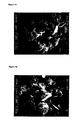
- Figures 1a and 1b show Scanning Electron Micrographs of copper and silver flakes, respectively, which are used.
- the flakes perform several functions. They form a skeleton structure in the printed image which holds the other ingredients together NDLIG> and prevents loss of resolution when the mixture is heated to cure it.
- the flakes naturally assume a lamellar structure like a stone wall which provides electrical conductivity in the direction parallel to the surface of the substrate and provides a framework to lessen the amount of metal transport necessary to achieve the well-consolidated pure metal conductors which are the objective of this invention. They also provide low surface energy, flat surfaces to which the other constituents of the composition can bond and on which metal can be deposited.
- the other metallic powder mixture constituent of the present invention are colloidal or semi-colloidal powders with diameters below 100 nanometers.
- the colloidal or semi-colloidal powder is preferably present in about 40% by weight of the total weight of the metal powder mixture.
- a primary function of these powders is to lower the temperature at which the compositions will consolidate to nearly solid pure metal conductors. The presence of fine metal powder has been found to be helpful in advancing this low temperature process with silver and essential to the consolidation of copper mixtures.
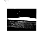
- Metal particles this small have a strong tendency to agglomerate into aggregates with an open skeletal structure as shown in Figure 2a.
- This is a copper powder produced by evaporating copper metal into inert gas where it condensed into particles of the desired size.
- the individual particles were totally agglomerated into large aggregates with a rigid skeletal structure which prevented consolidation of the mixtures made with the powder.
- Figure 2b shows a TEM of colloidal silver particles with a nominal diameter of 20 nanometers in an excellent state of dispersion. This material has been used in silver compositions and has lowered the critical consolidation temperature from 300 to 260 degrees C. These results and similar results with various copper powders are shown in Table 1.
- the Reactive Organic Medium provides the environment in which the metal powder mixture is bonded together to form well-consolidated conductors.
- Many classes of organic compounds can function as the ROM.
- the common characteristic which they share and which renders them effective is that they have, or can form, a bond to the metal via a hetero-atom.
- the hetero-atoms can be oxygen, nitrogen, sulfur, phosphorous, arsenic, selenium and other nonmetallic elements, preferably oxygen, nitrogen or sulfur. This bond is weaker than the bonds holding the organic moiety together, and can be thermally broken to deposit the metal.
- R - M ⁇ R + M where R is a reactive organic compound and M is the metal.
- R is a reactive organic compound and M is the metal.
- examples of such compounds are soaps of carboxylic acids, in which the hetero-atom is oxygen; amino compounds, in which the hetero-atom is nitrogen; and mercapto compounds, in which the hetero-atom is sulfur.
- ROM constituents are the carboxylic acids and the corresponding metallic soaps of neodecanoic acid and 2-ethyl hexanoic acid with silver and copper, such as silver neodecanoate illustrated by the formula: where R 1 , R 2 , and R 3 are C 9 H 19 and silver 2-ethyl hexanoate as illustrated by the formula: Gold amine 2-ethyl hexanoate is an example of a nitrogen compound.: Gold amine 2-ethyl hexanoate (gold amine octoate)
- Gold t-dodecyl mercaptide is an example of a sulfur compound: where R 1 , R 2 , and R 3 are C 11 H 23
- ROM compositions can be made by methods well known in the art. All of the above compounds are capable of decomposition to the respective metals at relatively low temperatures.
- the decomposition temperature is between 200 and 250°C .
- the corresponding copper compounds it is between 300 and 315 C.
- Gold sulfides decompose at very low temperatures in the neighborhood of 150°C .
- Gold amine octoate decomposes between 300 and 500°C .
- the copper and silver compounds can be reformed from the corresponding acids at the same temperature, so the reaction is reversible, as mentioned above.
- Alpha-terpineol has been used to reduce the viscosity of copper and silver compositions to facilitate screen printing.
- Alpha-terpineol also participates in the consolidation reaction by virtue of the acid character of the OH group bonded to an unsaturated ring.
- compositions of this invention have been applied by screening, stenciling, gravure printing, dispensing, ink jet printing and by coating an adhesive pattern with a dry powder composition or toner.
- Screening as used in applying conventional thick film pastes has been used most extensively for preparing samples for evaluation.
- a composition with a viscosity of approximately 500 poise is forced through a fine screen with a photo-defined open image of the desired conductor pattern in it by a rubber squeegee.
- the resolution which has been achieved by this method is approximately 125 micron (5 mil) lines and spaces, although production screen printers can achieve patterns as fine as 50 microns.
- Conductive traces with thicknesses up to 50 microns have been printed, though most of the test patterns have been in the neighborhood of 12 microns thick, which is equivalent to 0.37 ounces of copper per square foot.
- Preferred substrates include polymer-based substrates such as FR-4 glass reinforced epoxy laminate and coated polyimide films for silver compositions. Copper compositions, because of their higher curing temperature, are limited to the coated polyimides. Tested compounds would not adhere to bare polyimide films, although films treated in an oxygen plasma show some improvement. The reason is that adhesion is dependent on the chemical nature of the surface and some form of organic adhesive is necessary for good adhesion. This can be inherent in the chemistry of the surface as it appears to be in many epoxies. The silver compositions of this invention will adhere powerfully to FR-4 surfaces, even though the epoxy has been cured in the original lamination process. It is possible to apply the materials of his invention to one side of the laminate, oven cure it, apply another pattern to the other side, and cure again with no appreciable decrease in the adhesion achievable on the second side.
- the organic adhesive can be either thermoplastic or thermosetting.
- DuPont Kapton® FN which has been extensively used in developing the present compositions has a coating of FEP Teflon® on the surface which melts and bonds to the metal traces deposited by the present process.
- Kapton® KJ films have a surface coating of low glass transition point polyimide which can be softened to bond the present compositions in the temperature range of 220 to 350°C ..
- Polyamic acid coatings can be metallized with these compositions and cured to polyimide dielectric which insulates and bonds the conductors thus formed. Photoimageable epoxy-acrylate surfaces provide excellent adhesion after curing.
- Silver compositions containing only the metallo organic decomposition compound will adhere to silver plated or tinned copper surfaces or to those protected by an organic solder protectant such as benzotriazines.
- Silver compositions containing neodecanoic acid or other acids will also stick to bare copper. Copper compounds containing acids will bond well to bare copper.
- the adhesion measured in pull tests on various metal and substrate combinations is summarized in the accompanying table.
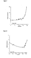
- the critical temperature for copper and silver mixtures is shown in Figures 5a and 5b. In both cases traces were screened onto Kapton substrates and held at the critical temperature for 60 seconds. For copper (and gold) the critical temperature is in excess of 300°C. It can be seen that between 305 and 325°C the resistivity of the traces drops by a factor of 100 to a value below 10 microohm-cm. The bulk resistivity of copper is 1.7 microohm-cm. At the same temperature at which the resistivity drops the mechanical properties of the traces improve equally dramatically.
- the critical temperature is approximately 230°C.
- a mixture of flake and acid only achieves some reduction in resistivity but only to 25-100 microohm cm similar to polymer thick film compositions in which the metal flakes are not well-bonded.
- the mixture contains metal flake plus colloidal metal powder plus tetradecane, an inert saturated hydrocarbon, in place of the reactive organic medium, the resistivity is poor and no consolidation takes place.
- the rate of sintering at 325° C can be expected to be lower than that at the usual thick film sintering temperature of 850°C by a factor of seventy million (7 x 10 7 ). A ten minute process at 850° C will take 1300 years at 325° C.
- compositions of the present invention consolidate as rapidly as they do at a temperature compatible with polymer-based substrates. It may be that the finely divided metal powders have a higher surface energy than bulk metal, and in the ROM environment in which it is processed, it is free of surface layers which would inhibit metal-to-metal contact and consolidation.
- the surface energy of the noble metals is as follows; Cu 1670 ergs. cm 2 @ 1047°C Ag 1140 ergs. cm 2 @ 907°C Au 1410 ergs. cm 2 @ 1027 °C (Chemistry in Two Dimensions-Surfaces, G.A. Somorjai, Cornell University Press, (1981)
- the metallo-organic compound decomposes directly onto the preexisting metal particles, welding them together by: AgCOOC 9 H 19 + Ag metal ⁇ More Ag metal ⁇ + organics ⁇ rather than by precipitation of new metal particles which then aggregate.
- the preexisting metal unquestionably provides a rigid framework, preventing shrinkage of the deposited metal and spreading of the molten ROM during decomposition which otherwise results in poor definition, poor adhesion and breaks in the traces.
- colloidal particles added to the compositions of this invention are themselves a source of additional metallo-organic by Ag colloid + HCOOC 9 H 19 ⁇ AgCOOC 9 H 19 providing a mechanism whereby the ROM can transport metal from high surface energy particles and edges to low surface area crevices and surfaces to consolidate the metal particles by a "chemical welding" process.
- the critical temperature can be adjusted by mixing metallo-organic constituents.
- gold amine octoate decomposes at temperatures up to 500°C . This is too high for use with polymer-based printed circuit substrates or most other electronic components.
- Gold t-dodecyl mercaptide decomposes at approximately 150°C. This is too low to bond effectively with the substrates of interest or with added gold flake.
- Gold neodecanoate decomposes at about 120-154°C.
- a mixture of gold amine octoate and gold neodecanoate has been used to achieve a decomposition temperature in the desirable range as described in Example 6 cited below.
- Both gold and silver mixtures can be heated in air since the elemental metals are the stable form at the temperature at which the metallo-organic constituent decomposes.
- Copper requires the use of a protective atmosphere to prevent the formation of copper oxide which is the stable product of decomposition in air.
- a nitrogen atmosphere containing less than about 20 and most preferably less than 3 ppm by volume of oxygen has been found to be suitable as shown in Figure 7.
- Addition of water vapor in the amount of about 5% has proven to be helpful in improving the conductivity of the resulting deposits as shown in Figure 8.
- Polymer thick film technology uses mixtures of carbon or metal powders or flakes in polymer adhesives, primarily epoxies, to make printable mixtures. These can be applied to polymer substrates and cured at temperatures up to 176°C to create conductor patterns in the same way that thick film inks and pastes are applied to ceramic and glass substrates at higher temperatures.
- Polymer metallizing is used to provide a conductive layer on polymer parts such as desk top computer housings, usually for electrical shielding. Again, carbon or metal particles are suspended in a paint or other organic coating material.
- the carbon coatings are substantially less electrically conducting than the metal-based coatings.
- the best are silver flake-loaded epoxies which can have resistivities as low as 50-60 microohm-cm.
- the present invention provides an alternative to conventional polymer thick film compositions which can be cured at a temperature which a polymer-based substrate can withstand, while providing an electrical conductivity comparable to the pure metal and at least a factor of ten greater than the best polymer thick films.
- compositions of this invention may be applied to the adhesive-coated polymer substrates by any convenient printing process.
- An advantage of printable metallization compounds is that three dimensional objects can be metallized which is not possible with metal foil and very difficult with sputtered or evaporated metal.
- Wire coating can be carried out continuously in equipment analogous to wire enameling towers.
- An example of this application is recited below in Example 10.
- the heat treating process is done under conditions very similar to soldering and in similar equipment. Additional cost savings can be realized by combining the curing of crossover traces and attachment of components. This is accomplished by printing additional material on the attachment pads for the components to be mounted on the circuit, placing the components on the uncured material with optional addition of additional material to the components themselves by printing or dipping, and heat treating the assembly to simultaneously consolidate and bond the additional traces and bond the components to the circuit, as shown in Figure 9b
- the presently disclosed technology can be combined with photo sensitive materials to create a hybrid technology, as shown in Figure 9 c.
- a photosensitive resist or solder mask is applied to the surface of the circuit and exposed to the desired pattern of conductor traces, which can be very fine.
- the negative image is developed in the usual way be washing the unpolymerized, unexposed material away.
- the mixture of the present disclosure is applied by printing or doctor blading it into the circuit traces. Components may be placed at this stage if desired to make the circuit traces and assemble the circuit simultaneously, as described above.
- the circuit is heat treated in an oven which consolidates the mixture and completely polymerizes the resist or solder mask into an infusible, insoluble dielectric.
- An additional layer of solder mask or potting compound can be applied to protect the finished circuit in the usual way.
- Most contemporary printed circuits are multilayers with attachment pads for components on the two surfaces and the bulk of the circuit connections on thin inner layers. The latter are laminated between the two surface layers to make the completed multilayer.
- Inner layers are produced by the same technology as outer layers and conventional single sided and double sided printed wiring boards.
- the inner layer substrate is similar to conventional glass reinforced epoxy FR-4 material but much thinner. The minimum is about 0.004 inches thick, limited by the fact that it is conventional to use two layers of glass fabric to avoid single strands of glass going from side to side and acting as potential short circuit paths.
- the epoxy-glass is laminated to copper foil on one or both sides to provide the electrical conductors to be developed by etching and/or plating.
- the copper clad substrate is laminated to a dry film resist or coated with a liquid resist. It is then exposed to ultraviolet light to partially polymerize the resist, which is usually an acrylic-epoxy mixture. The unexposed resist is removed by a weak caustic or solvent wash to develop a negative image. The image is then converted to circuitry by etching away the exposed copper to leave circuit traces protected by resist which is stripped by strong caustic.
- An alternative method is to electroplate copper followed by tin-lead etch resist on the exposed copper, strip the polymer resist and etch away the unprotected original copper foil.
- the finished inner layers are stacked with the outer layers on the outside of the stack and with interleaving sheets of "prepreg" which is, again, two layers of glass cloth impregnated with B-stage epoxy resin .
- the stack is then cured in a laminating press typically at 400 psi, 350°F for an hour. Often a vacuum press is used to remove entrained air and improve quality.
- compositions and processes of this invention replace this complexity with a simple print-and-heat technique which can produce inner layers very rapidly and very economically.
- the inner layer material is simply cleaned, printed and heat treated in an oven to convert the image to circuit conductors.
- the printed layers are then laminated in the usual way.
- the conductor pattern can be applied to a continuous web of substrate by a rotary press, much like printing a newspaper but with finer resolution, as shown in Figure 10 a.
- Gravure printing can be used in this application. Offset printing can produce very high resolution also.
- Ink jet printing and electrostatic printing at high speeds are candidates.
- the circuits will be cured in an oven, still as a continuous web. The ability of these mixtures to cure to solid metal in seconds is critical to realizing this concept. Longer processing times would make the oven disproportionately large relative to the press and squander much of the speed advantage of high speed printing.
- ICs Integrated Circuits
- PWBs Printed Wiring Boards
- the conventional method of packaging ICs is to cement them into a ceramic or plastic chip carrier and wire bond the individual input/output pads on the IC to individual pins on a metal lead frame.
- the IC is then potted in plastic or ceramic and covered with a lid for protection.
- the leads are separated from the frame and bent to shape for insertion into a socket or for soldering directly to pads on the PWB (surface mount technology).
- TAB Tape Automated Bonding
- Some Chip on Board (COB) direct attachment is done by wire bonding the IC to pads on the PWB, but this, while conventional and reliable, is expensive and time consuming.
- Both TAB bonding and the more advanced COB applications are gang bonded by "bumping" the pads on the IC with added metal and soldering the bumps to mating pads on the tape or the PWB.
- the bumping process itself is time-consuming and expensive because it is done by depositing a number of metallic layers under vacuum using photolithographic techniques. Preparing the tapes or circuit pads is expensive because it is at the limit of resolution of conventional subtractive etching technology with 50 micron (0.002 inch) lines and spaces.
- the tapes are further processed to remove the polymer in the center portion leaving very fine and fragile metal fingers pointing in toward the IC which can be individually bonded to the pads.
- a technology in which ICs could be gang bonded to traces on a PWB or a polyimide tape in a single operation could achieve a major simplification and cost reduction.
- the compositions of the present invention can be applied to ICs and/or to polymer-based substrates to act as a bonding agent to secure the IC to the substrate with all the electrical connections made simultaneously and reliably.
- the pads on ICs are almost universally made of aluminum, which is compatible with the silicon semiconductor, is a good electrical conductor and is easily and economically applied by evaporation or sputtering.
- Aluminum is not easy to bond to due to the very tenacious native oxide which protects the aluminum surface from oxidation and corrosion. Wire bonding and chip bumping have to overcome this obstacle to obtain reliable bonds.
- wire bonding the connections are made to balls formed on the end of 0.001 inch diameter gold wire by welding them to the aluminum, usually by ultrasonic agitation to mechanically disrupt the oxide film and cold weld the gold to the aluminum.
- a layer of an intermediate bonding metal such as titanium-tungsten alloy is deposited by sputtering to make contact with the aluminum and isolate it from the material of the bump which is deleterious to the silicon.
- Other-layers are added as well as the copper or solder bump material. All of these operations require photolithographic masking and are quite expensive.
- a polyimide insulating layer is often applied to the surface of the chip to protect it from the subsequent processing by covering all but the pads .
- compositions of this invention may be applied to the IC by any convenient printing process. Tests have been done by screen printing conductor images. The mixtures have also been applied by stenciling and ink jet printing. Gravure printing, both direct and offset can be used to produce fine line images. Offset lithography can be used, as can direct impressions by rubber or metal plates. If a mixture can be found which will bond directly to aluminum without the gold or other bonding layer, a particularly elegant lithographic method can be used.
- the compositions of this invention do not stick to untreated polyimide surfaces.
- the IC can be coated with polyimide and patterned to expose the pads as before. The composition can then be applied by doctor blading it across the surface or by a rough printing process with poorer resolution than the pads.
- the composition will detach from the polyimide surface and bead up on the aluminum pads producing the exact structure desired with higher resolution than the printing process used to apply it.
- a mixture might include fluoride based fluxes to dissolve the aluminum oxide layer during the heat treating process.
- the same process could be used to mask off and print very fine conductors on the surface of the semiconductor IC itself to connect pads or reroute I/O leads.
- the bumped chips of this invention must be attached either to a polyimide tape or a PWB with matching metallic circuit traces.
- Such traces may be produced by the methods of this invention by a simple print-and-heat process with high resolution Additional printing processes are applicable to polymer films which are not applicable to ICs.
- electrostatic methods xerography
- ink jet printing provides the ability to generate conductor patterns direct from CAD files. This provides great flexibility in design and in small quantity manufacture and inventory control.
- the highest possible resolution is provided by photolithographic techniques and a hybrid technology in which the dielectric is patterned photographically and a composition of this invention is printed or doctored into the grooves is a highly reliable and promising way to produce very fine conductor patterns for TAB and direct attach.
- the method is the same as method B described above for patterning the chip and the method shown in Figure 9 c above.
- the next highest resolution may be provided by electrostatic printing with liquid toner suspensions with particle diameters of a few microns.
- S.P. Schmidt, et al. "Handbook of Imaging Materials", Chapter 5, pp. 227-252, A.S. Daimond, Ed., (Marcel Dekker, NY).
- the bonding process may be carried out in several ways.
- the image is converted to metal by heating in an oven.
- Example 1 Copper composition with copper flake, copper powder, and acid.
- a composition has been prepared for producing conductive copper traces on dielectric substrates.
- the electrical resistivity of the circuit trace (23.7 cm long, 0.4 mm wide) was calculated to be 5 microohm-cm by measuring the resistance of the trace and weighing the amount of metal deposited. The mass divided by the density gives the total volume of metal. Scotch tape was applied to the circuit trace and immediately removed at a 90 degree angle to determine the bond strength of the copper to the substrate. No metal was removed with the tape.
- a composition has been prepared for producing conductive copper traces on dielectric substrates to show the detrimental effect of eliminating the colloidal copper powder ingredient.
- circuit trace After heating, the circuit trace was dry to the touch, the organic constituents having been completely removed.
- the electrical resistivity of the circuit trace was calculated to be 24 microohm-cm. Scotch tape was applied to the circuit trace and immediately removed at a 90 degree angle to determine the bond strength of the copper to the substrate. Some of the copper was removed with the tape.
- Example 3 Copper powder and acid.
- a composition has been prepared for producing conductive copper traces on dielectric substrates illustrating the detrimental effect of eliminating the copper flake ingredient.
- circuit trace After heating, the circuit trace was dry to the touch, the organic constituents having been completely removed. The circuit trace was not continuous, thus it did not conduct electricity. Scotch tape was applied to the circuit trace and immediately removed at a 90 degree angle to determine the bond strength of the copper to the substrate. No metal was removed with the tape.
- Example 4 Copper flake, copper powder, and tetradecane.
- a composition has been prepared for producing conductive copper traces on dielectric substrates showing the detrimental effect of substituting an unreactive saturated hydrocarbon for the Reactive Organic Medium.
- circuit trace After heating, the circuit trace was dry to the touch, the organic constituents having been completely removed.
- the electrical resistivity of the circuit trace (23.7 cm long, 0.4 mm wide) was calculated to be 25 microohm-cm.
- Scotch tape was applied to the circuit trace and immediately removed at a 90 degree angle to determine the bond strength of the copper to the substrate. Some of the copper was removed with the tape.
- a composition has been prepared for producing conductive silver traces on dielectric substrates containing silver flake, a silver metallo-organic decomposition compound and a reactive rheology modifier.
- circuit trace After heating, the circuit trace was dry to the touch, the organic constituents having been completely removed.
- the electrical resistivity of the circuit trace (23.7 cm long, 0.4 mm wide) was calculated to be 3.7 microohm-cm. Scotch tape was applied to the circuit trace and immediately removed at a 90 degree angle to determine the bond strength of the silver to the substrate. No metal was removed.
- Example 6 Silver flake, silver neodecanoate, and acid
- a composition has been prepared for producing conductive silver traces on dielectric substrates and on copper surfaces with neodecanoic acid as a reactive rheology modifier and flux.
- circuit trace After heating, the circuit trace was dry to the touch, the organic constituents having been completely removed.
- the electrical resistivity of the circuit trace (23.7 cm long, 0.4 mm wide) was calculated to be 3.2 microohm-cm. Scotch tape was applied to the circuit trace and immediately removed at a 90 degree angle to determine the bond strength of the silver to the substrate. No metal was removed.
- Example 7 Gold flake, gold neodecanoate, and gold amine octoate
- a composition has been prepared for producing conductive gold traces on dielectric substrates with a ROM containing two metallo-organic decomposition compounds for temperature optimization.
- circuit trace After heating, the circuit trace was dry to the touch, the organic constituents having been completely removed.
- the electrical resistivity of the circuit trace (23.7 cm long, 0.4 mm wide) was calculated to be 7.4 microohm-cm. Scotch tape was applied to the circuit trace and immediately removed at a 90 degree angle to determine the bond strength of the gold to the substrate. No metal was removed.
- a composition has been prepared for producing conductive silver traces on glass-reinforced epoxy dielectric substrates.
- circuit trace After heating, the circuit trace was dry to the touch, the organic constituents having been completely removed.
- the electrical resistivity of the circuit trace (23.7 cm long, 0.4 mm wide) was calculated to be 3.2 microohm-cm. Scotch tape was applied to the circuit trace and immediately removed at a 90 degree angle to determine the bond strength of the silver to the substrate. No metal was removed.
- a composition has been prepared for producing conductive copper traces on polyimide-coated dielectric substrates.
- circuit trace After heating, the circuit trace was dry to the touch, the organic constituents having been completely removed.
- the electrical resistivity of the circuit trace (23.7 cm long, 0.4 mm wide) was calculated to be 4.5 microohm-cm.
- Scotch tape was applied to the circuit trace and immediately removed at a 90 degree angle to determine the bond strength of the copper to the substrate. No metal was removed with the tape.
- a silver composition has been prepared for producing conductive silver traces on dielectric substrates.
- circuit trace After heating, the circuit trace was dry to the touch, the organic constituents having been completely removed.
- the electrical resistivity of the circuit trace (23.7 cm long, 0.4 mm wide) was calculated to be 3.1 microohm-cm. Scotch tape was applied to the circuit trace and immediately removed at a 90 degree angle to determine the bond strength of the silver to the substrate. No metal was removed.
- a composition has been prepared for producing conductive copper traces bonded to copper foil.
- Example 6 The composition of Example 6 has been applied to copper clad glass-reinforced epoxy substrates.
- circuit trace After heating, the circuit trace was dry to the touch, the organic constituents having been completely removed. Scotch tape was applied to the circuit trace and immediately removed at a 90 degree angle to determine the bond strength of the silver to the substrate. No metal was removed.
- An example of a mixture which has been used for experiments on polymer metallization is one made up of 12 parts silver flake, 3 parts silver neodecanoate and 1.8 parts ⁇ -terpineol by weight prepared as described in the previous examples.
- a demonstration of polymer metallizing using this composition has been carried out by applying a shielding coating to wire-wrap wire.
- Kynar-insulated #30 wire was coated by rubbing with the silver mixture described above and cured in an oven at 277 C. The resulting silver coating was firmly attached to the wire.
- the wire could be tied in an overhand knot and drawn tight without flaking the coating off.
- a linear resistance of 0.2 ohms per cm was achieved with a coating of 0.0006 grams of silver per cm, equivalent to a resistivity of 12 microohm-cm.
- Example 14 Polymer metallization.
- compositions and methods of the present invention offer a wholly new approach to creating fully additive electronic circuitry.
- Figure 12 shows a comparison of the electrical resistivity of traces made by the method of this invention compared to those of prior art methods along with the respective processing conditions of temperature and curing time. It can be seen that the present invention provides conductivity (and solderability) equivalent to conventional thick film processing but at a temperature hundreds of degrees lower. It is compatible with polymer substrates but offers orders of magnitude better electrical conductivity and processing speed than existing polymer thick film and transient liquid phase alternatives.
Landscapes
- Chemical & Material Sciences (AREA)
- Chemical Kinetics & Catalysis (AREA)
- Engineering & Computer Science (AREA)
- Organic Chemistry (AREA)
- Dispersion Chemistry (AREA)
- Polymers & Plastics (AREA)
- Medicinal Chemistry (AREA)
- Health & Medical Sciences (AREA)
- Microelectronics & Electronic Packaging (AREA)
- Spectroscopy & Molecular Physics (AREA)
- Physics & Mathematics (AREA)
- Nanotechnology (AREA)
- Conductive Materials (AREA)
- Parts Printed On Printed Circuit Boards (AREA)
- Manufacturing Of Printed Wiring (AREA)
- Powder Metallurgy (AREA)
- Macromonomer-Based Addition Polymer (AREA)
- Organic Insulating Materials (AREA)
Claims (15)
- Materiezusammensetzung, die folgendes umfaßt:(a) eine Metallpulvermischung, die folgendes umfaßt:(i) Metallflocken mit einem Durchmesser zwischen 2 und 10 Mikrometern und einer Dicke von weniger als 1 Mikrometer und(ii) kolloidalen Metallteilchen mit einem Durchmesser von unter 0,1 Mikrometer und(b) ein reaktives organisches Medium, das eine Bindung zu dem Metall über ein Heteroatom aufweist oder ausbilden kann und ausgewählt ist aus der Gruppe bestehend aus einer metallorganischen Zersetzungsverbindung, einer reaktiven Verbindung, die mit der Metallpulvermischung reagieren kann unter Erzeugung der metallorganischen Zersetzungsverbindung, und einer Mischung aus der metallorganischen Zersetzungsverbindung und der reaktiven Verbindung;wobei die Zusammensetzung auf ein Substrat aufgebracht werden kann und wobei das reaktive organische Medium mit der Metallpulvermischung reagiert und sich bei einer Temperatur unter 450°C unter Ausbildung eines massiven reinen Metalleiters zersetzt.
- Zusammensetzung nach Anspruch 1, wobei das reaktive organische Medium aus einer oder mehreren reaktiven organischen Verbindungen mit jeweils einer anderen Zersetzungstemperatur besteht, wobei das reaktive organische Medium eine Zersetzungstemperatur aufweist, die von jeder der reaktiven organischen Verbindungen verschieden ist.
- Zusammensetzung nach Anspruch 1, wobei die Metallflocken einen Durchmesser von etwa 5 Mikrometern aufweisen.
- Zusammensetzung nach Anspruch 1, wobei das reaktive organische Medium eine organische Gruppierung umfaßt, die durch chemische Bindungen zusammengehalten wird, und wobei die Bindung zu dem Metall über das Heteroatom schwächer ist als die Bindungen, die die organische Gruppierung zusammenhalten, und thermisch gebrochen werden kann.
- Zusammensetzung nach Anspruch 1, bei der das Metall ausgewählt ist aus der Gruppe bestehend aus Kupfer, Silber, Gold, Zink, Cadmium, Palladium, Iridium, Ruthenium, Osmium, Rhodium, Platin, Eisen, Kobalt, Nickel, Indium, Zinn, Antimon, Blei und Bismut.
- Verfahren zum Produzieren von massiven reinen Metalleitern auf einem Substrat, umfassend die folgenden Schritte:(A) Aufbringen eines Leitervorläufers in dem gewünschten Muster auf dem Substrat und(B) Erhitzen des Substrats in einem Ofen auf eine kritische Temperatur unter 450°C für eine Zeit von weniger als etwa 5 Minuten;wobei das aufgebrachte Leitervorläufermuster aus einem reaktiven organischen Medium und einer Metallpulvermischung besteht,
wobei das reaktive organische Medium eine Bindung zu dem Metall über ein Heteroatom aufweist oder ausbilden kann und ausgewählt ist aus der Gruppe bestehend aus einer metallorganischen Zersetzungsverbindung, einer reaktiven Verbindung, die mit der Metallpulvermischung reagieren kann unter Erzeugung der metallorganischen Zersetzungsverbindung, und einer Mischung aus der metallorganischen Zersetzungsverbindung und der reaktiven Verbindung, und
wobei die Metallpulvermischung folgendes umfaßt:(i) Metallflocken mit einem Durchmesser zwischen 2 und 10 Mikrometern und einer Dicke von weniger als 1 Mikrometer und(ii) kolloidalen Metallteilchen mit einem Durchmesser von unter 0,1 Mikrometer undwobei das reaktive organische Medium mit der Metallpulvermischung reagiert und sich bei einer Temperatur unter 450°C unter Ausbildung eines massiven reinen Metalleiters zersetzt. - Verfahren nach Anspruch 6, wobei der Leitervorläufer auf dem Substrat aufgebracht wird durch eine Technologie ausgewählt aus der Gruppe bestehend aus: Siebdruck, Schablonendruck, Gravurdruck, Prägedruck, Offsetdruck, lithographischer Druck, Dispensieren, Rakeln, Tintenstrahldruck, xerographisches Kopieren und elektrostatischer Druck.
- Verfahren nach Anspruch 6, bei dem der Leitervorläufer eine kupferbasierte Zusammensetzung ist und bei dem die Ofenatmosphäre Stickstoff ist mit weniger als 20 Volumenteilen pro Million Sauerstoff, bevorzugt weniger als 3 Teilen pro Million.
- Verfahren nach Anspruch 8, bei dem Wasserdampf dem Stickstoff in einem Ausmaß von etwa 5 mol-% während der Periode zugesetzt wird, in der der Leitervorläufer erhitzt wird, aber nicht vor oder nach der Erhitzungsphase.
- Verfahren nach Anspruch 6, wobei das Substrat ein Polymer umfaßt, das sich bei Temperaturen über 450°C zersetzt.
- Verfahren nach Anspruch 6, wobei das Substrat einen Halbleiter umfaßt, der sich bei Temperaturen über 450°C zersetzt.
- Verfahren nach Anspruch 6, bei dem der Leitervorläufer auf Metalleiter und dielektrische Isolatoren aufgebracht wird, um elektrische Verbindungen zwischen den Leitern herzustellen.
- Verfahren nach Anspruch 6, bei dem der Leitervorläufer in Schritt A) auf ein photostrukturierbares dielektrisches Material aufgebracht wird, das durch Photolithographie strukturiert worden ist, um Kanäle zu definieren, die Leiter werden sollen, wobei die Kanäle mit dem Leitervorläufer durch Rakeln oder Drucken gefüllt werden, wobei die Erhitzung von Schritt B) gleichzeitig das dielektrische Material vernetzt und das aufgebrachte Leitervorläufermuster konsolidiert.
- Verfahren nach Anspruch 6, bei dem der Leitervorläufer in Schritt A) auf eine kontinuierliche Bahn aus dünnem Substratmaterial aufgebracht und in Schritt B) als eine kontinuierliche Bahn in einem Ofen gehärtet wird, weiter umfassend den folgenden Schritt:C) Zuschneiden der kontinuierlichen Bahn aus dünnem Substratmaterial zu einem Endprodukt.
- Verfahren nach Anspruch 6, bei dem der Leitervorläufer auf Halbleiterbauelemente aufgebracht wird, um elektrische Leiterbahnen und Bumps auf der Halbleiteroberfläche herzustellen.
Applications Claiming Priority (15)
| Application Number | Priority Date | Filing Date | Title |
|---|---|---|---|
| US3845397P | 1997-02-20 | 1997-02-20 | |
| US3867097P | 1997-02-20 | 1997-02-20 | |
| US3866997P | 1997-02-20 | 1997-02-20 | |
| US3851497P | 1997-02-20 | 1997-02-20 | |
| US38453P | 1997-02-20 | ||
| US38514P | 1997-02-20 | ||
| US38670P | 1997-02-20 | ||
| US38669P | 1997-02-20 | ||
| US4654197P | 1997-05-15 | 1997-05-15 | |
| US4654097P | 1997-05-15 | 1997-05-15 | |
| US4655297P | 1997-05-15 | 1997-05-15 | |
| US46541P | 1997-05-15 | ||
| US46552P | 1997-05-15 | ||
| US46540P | 1997-05-15 | ||
| PCT/US1997/016226 WO1998037133A1 (en) | 1997-02-20 | 1997-09-12 | Low temperature method and compositions for producing electrical conductors |
Publications (3)
| Publication Number | Publication Date |
|---|---|
| EP0961809A1 EP0961809A1 (de) | 1999-12-08 |
| EP0961809A4 EP0961809A4 (de) | 2004-07-21 |
| EP0961809B1 true EP0961809B1 (de) | 2007-02-07 |
Family
ID=27567891
Family Applications (1)
| Application Number | Title | Priority Date | Filing Date |
|---|---|---|---|
| EP97941061A Expired - Lifetime EP0961809B1 (de) | 1997-02-20 | 1997-09-12 | Niedertemperaturverfahren und zusammensetzungen zur herstellung elektischer leiter |
Country Status (8)
| Country | Link |
|---|---|
| EP (1) | EP0961809B1 (de) |
| JP (1) | JP3585244B2 (de) |
| KR (1) | KR100532734B1 (de) |
| AT (1) | ATE353536T1 (de) |
| AU (1) | AU4269697A (de) |
| CA (1) | CA2280115C (de) |
| DE (1) | DE69737328T2 (de) |
| WO (1) | WO1998037133A1 (de) |
Cited By (1)
| Publication number | Priority date | Publication date | Assignee | Title |
|---|---|---|---|---|
| EP2003940A2 (de) | 2007-06-14 | 2008-12-17 | manroland AG | Drucktechnisch hergestellte funktionale Komponenten |
Families Citing this family (44)
| Publication number | Priority date | Publication date | Assignee | Title |
|---|---|---|---|---|
| US7625420B1 (en) | 1997-02-24 | 2009-12-01 | Cabot Corporation | Copper powders methods for producing powders and devices fabricated from same |
| US6143356A (en) * | 1999-08-06 | 2000-11-07 | Parelec, Inc. | Diffusion barrier and adhesive for PARMOD™ application to rigid printed wiring boards |
| TW511122B (en) * | 1999-12-10 | 2002-11-21 | Ebara Corp | Method for mounting semiconductor device and structure thereof |
| KR100940110B1 (ko) * | 1999-12-21 | 2010-02-02 | 플라스틱 로직 리미티드 | 잉크젯으로 제조되는 집적회로 및 전자 디바이스 제조 방법 |
| JP4596444B2 (ja) * | 2001-03-23 | 2010-12-08 | 大日本印刷株式会社 | オフセット印刷による電極パターンの形成方法 |
| DE60124433T2 (de) * | 2001-06-28 | 2007-09-06 | Parelec, Inc. | Tieftemperaturverfahren und zusammensetzungen zur herstellung elektrischer leiter |
| US6591496B2 (en) | 2001-08-28 | 2003-07-15 | 3M Innovative Properties Company | Method for making embedded electrical traces |
| US7629017B2 (en) | 2001-10-05 | 2009-12-08 | Cabot Corporation | Methods for the deposition of conductive electronic features |
| US7524528B2 (en) | 2001-10-05 | 2009-04-28 | Cabot Corporation | Precursor compositions and methods for the deposition of passive electrical components on a substrate |
| US6951666B2 (en) | 2001-10-05 | 2005-10-04 | Cabot Corporation | Precursor compositions for the deposition of electrically conductive features |
| US7553512B2 (en) | 2001-11-02 | 2009-06-30 | Cabot Corporation | Method for fabricating an inorganic resistor |
| KR100884995B1 (ko) * | 2002-06-12 | 2009-02-20 | 엘지디스플레이 주식회사 | 액정표시장치의 공정라인 및 이를 이용한 제조방법 |
| KR20060012545A (ko) * | 2002-07-03 | 2006-02-08 | 나노파우더스 인더스트리어스 리미티드. | 저온 소결처리한 전도성 나노 잉크 및 이것의 제조 방법 |
| US20040178391A1 (en) * | 2003-01-29 | 2004-09-16 | Conaghan Brian F. | High conductivity inks with low minimum curing temperatures |
| KR100545288B1 (ko) | 2003-03-28 | 2006-01-25 | 주식회사 잉크테크 | 유기은 조성물 및 그 제조방법, 그로부터 제조되는 잉크및 그 잉크를 이용한 도전배선 형성 방법 |
| CN100542692C (zh) * | 2003-07-09 | 2009-09-23 | 福莱金属公司 | 包覆金属颗粒 |
| EP2166543B1 (de) * | 2003-09-02 | 2011-03-23 | Plastic Logic Limited | Herstellung von elektronischen Geräten |
| GB0320491D0 (en) | 2003-09-02 | 2003-10-01 | Plastic Logic Ltd | Multi-level patterning |
| GB0324561D0 (en) * | 2003-10-22 | 2003-11-26 | Koninkl Philips Electronics Nv | A method of producing a conductive layer on a substrate |
| JP4549655B2 (ja) * | 2003-11-18 | 2010-09-22 | メルク パテント ゲゼルシャフト ミット ベシュレンクテル ハフツング | 機能性塗料 |
| KR100872162B1 (ko) * | 2004-04-14 | 2008-12-08 | (주)석경에이.티 | 도전성 금속 나노입자 및 이를 포함하는 나노금속 잉크 |
| JP4628718B2 (ja) * | 2004-07-23 | 2011-02-09 | 株式会社フジクラ | 導電性被膜の形成方法 |
| US7824466B2 (en) | 2005-01-14 | 2010-11-02 | Cabot Corporation | Production of metal nanoparticles |
| US8167393B2 (en) | 2005-01-14 | 2012-05-01 | Cabot Corporation | Printable electronic features on non-uniform substrate and processes for making same |
| TW200640596A (en) | 2005-01-14 | 2006-12-01 | Cabot Corp | Production of metal nanoparticles |
| US7533361B2 (en) | 2005-01-14 | 2009-05-12 | Cabot Corporation | System and process for manufacturing custom electronics by combining traditional electronics with printable electronics |
| US8334464B2 (en) | 2005-01-14 | 2012-12-18 | Cabot Corporation | Optimized multi-layer printing of electronics and displays |
| CA2619997C (en) | 2005-08-24 | 2013-08-13 | A.M. Ramp & Co. Gmbh | Process for producing articles having an electrically conductive coating |
| JP2007084384A (ja) * | 2005-09-22 | 2007-04-05 | Seiko Epson Corp | セラミックス電子部品の製造方法およびセラミックス電子部品 |
| JP2007088221A (ja) * | 2005-09-22 | 2007-04-05 | Seiko Epson Corp | セラミックス電子部品の製造方法およびセラミックス電子部品 |
| KR100707911B1 (ko) * | 2006-05-23 | 2007-04-13 | (주)석경에이.티 | 도전성 금속 나노입자 및 이를 포함하는 나노금속 잉크 |
| JP2006270118A (ja) * | 2006-05-29 | 2006-10-05 | Morimura Chemicals Ltd | 回路基板の製造方法 |
| JP2006229254A (ja) * | 2006-05-29 | 2006-08-31 | Morimura Chemicals Ltd | 透光体の製造方法 |
| KR100790457B1 (ko) * | 2006-07-10 | 2008-01-02 | 삼성전기주식회사 | 금속 나노입자의 제조방법 |
| KR100711505B1 (ko) | 2007-01-30 | 2007-04-27 | (주)이그잭스 | 도전막 형성을 위한 은 페이스트 |
| KR100889489B1 (ko) * | 2008-03-18 | 2009-03-19 | 주식회사하이퍼플렉스 | 도전성 섬유재를 갖는 연성 회로기판 및 이를 갖는전자제품 |
| KR101180475B1 (ko) * | 2009-02-05 | 2012-09-07 | 주식회사 엘지화학 | 전도성 패턴의 형성방법 및 이에 의하여 제조된 전도성 패턴을 갖는 기판 |
| KR101132108B1 (ko) | 2009-02-18 | 2012-04-05 | 도요 보세키 가부시키가이샤 | 금속 박막 제조 방법 및 금속 박막 |
| KR101276237B1 (ko) * | 2010-12-02 | 2013-06-20 | 한국기계연구원 | 저온소결 전도성 금속막 및 이의 제조방법 |
| JP5598739B2 (ja) * | 2012-05-18 | 2014-10-01 | 株式会社マテリアル・コンセプト | 導電性ペースト |
| US11111396B2 (en) * | 2014-10-17 | 2021-09-07 | C3 Nano, Inc. | Transparent films with control of light hue using nanoscale colorants |
| US20170252804A1 (en) * | 2016-03-04 | 2017-09-07 | Lockheed Martin Corporation | Additive manufacturing processes utilizing metal nanoparticles |
| DE102019124954A1 (de) * | 2019-09-17 | 2021-03-18 | Danfoss Silicon Power Gmbh | Verfahren zum Verbinden eines ersten elektronischen Bauteils mit einem zweiten elektronischen Bauteil |
| KR20220028553A (ko) | 2020-08-28 | 2022-03-08 | (주)합동하이텍그라스 | 투과율 가변 필름 및 그 제조 방법 |
Family Cites Families (6)
| Publication number | Priority date | Publication date | Assignee | Title |
|---|---|---|---|---|
| US4122143A (en) * | 1976-05-24 | 1978-10-24 | Mitsui Toatsu Chemicals, Inc. | Process for producing cured products |
| JPH0797696B2 (ja) * | 1986-07-05 | 1995-10-18 | 株式会社豊田自動織機製作所 | ハイブリツドic基板と回路パタ−ン形成方法 |
| US4808274A (en) * | 1986-09-10 | 1989-02-28 | Engelhard Corporation | Metallized substrates and process for producing |
| JPH0747233B2 (ja) * | 1987-09-14 | 1995-05-24 | 古河電気工業株式会社 | 半田析出用組成物および半田析出方法 |
| DE3919564C2 (de) * | 1989-06-15 | 1993-10-07 | Bosch Gmbh Robert | Verfahren zum Herstellen von Leiterbahnen auf einer Polyimidfolie |
| US5059242A (en) * | 1990-04-27 | 1991-10-22 | Firmstone Michael G | Seed layer compositions containing organogold and organosilver compounds |
-
1997
- 1997-09-12 AT AT97941061T patent/ATE353536T1/de not_active IP Right Cessation
- 1997-09-12 JP JP53236498A patent/JP3585244B2/ja not_active Expired - Fee Related
- 1997-09-12 CA CA002280115A patent/CA2280115C/en not_active Expired - Fee Related
- 1997-09-12 DE DE69737328T patent/DE69737328T2/de not_active Expired - Fee Related
- 1997-09-12 AU AU42696/97A patent/AU4269697A/en not_active Abandoned
- 1997-09-12 WO PCT/US1997/016226 patent/WO1998037133A1/en not_active Ceased
- 1997-09-12 KR KR10-1999-7007608A patent/KR100532734B1/ko not_active Expired - Fee Related
- 1997-09-12 EP EP97941061A patent/EP0961809B1/de not_active Expired - Lifetime
Cited By (3)
| Publication number | Priority date | Publication date | Assignee | Title |
|---|---|---|---|---|
| EP2003940A2 (de) | 2007-06-14 | 2008-12-17 | manroland AG | Drucktechnisch hergestellte funktionale Komponenten |
| EP2003941A2 (de) | 2007-06-14 | 2008-12-17 | manroland AG | Drucktechnisch hergestellte funktionale Komponenten |
| DE102007027473A1 (de) | 2007-06-14 | 2008-12-18 | Manroland Ag | Drucktechnisch hergestellte funktionale Komponenten |
Also Published As
| Publication number | Publication date |
|---|---|
| CA2280115A1 (en) | 1998-08-27 |
| AU4269697A (en) | 1998-09-09 |
| JP3585244B2 (ja) | 2004-11-04 |
| EP0961809A1 (de) | 1999-12-08 |
| CA2280115C (en) | 2007-11-13 |
| JP2001515645A (ja) | 2001-09-18 |
| EP0961809A4 (de) | 2004-07-21 |
| KR100532734B1 (ko) | 2005-11-30 |
| DE69737328T2 (de) | 2007-11-22 |
| KR20000075549A (ko) | 2000-12-15 |
| ATE353536T1 (de) | 2007-02-15 |
| WO1998037133A1 (en) | 1998-08-27 |
| DE69737328D1 (de) | 2007-03-22 |
Similar Documents
| Publication | Publication Date | Title |
|---|---|---|
| EP0961809B1 (de) | Niedertemperaturverfahren und zusammensetzungen zur herstellung elektischer leiter | |
| US6379745B1 (en) | Low temperature method and compositions for producing electrical conductors | |
| US7115218B2 (en) | Low temperature method and composition for producing electrical conductors | |
| US6036889A (en) | Electrical conductors formed from mixtures of metal powders and metallo-organic decomposition compounds | |
| US6143356A (en) | Diffusion barrier and adhesive for PARMOD™ application to rigid printed wiring boards | |
| US11699632B2 (en) | Methods for attachment and devices produced using the methods | |
| US6743319B2 (en) | Adhesiveless transfer lamination method and materials for producing electronic circuits | |
| US5039552A (en) | Method of making thick film gold conductor | |
| EP1827066A2 (de) | Elektronenanlagerungsunterstützte Erzeugung elektrischer Leiter | |
| WO1996024938A1 (en) | Composite conductive powder, conductive paste, method of producing conductive paste, electric circuit and method of fabricating electric circuit | |
| EP1410403B1 (de) | Tieftemperaturverfahren und zusammensetzungen zur herstellung elektrischer leiter | |
| WO1999016601A1 (en) | Manufacture of thin metal objects | |
| JP3222950B2 (ja) | 強固なはんだ付け可能な導電性ペースト | |
| WO1999017352A1 (en) | Method and compositions for metallizing microvias and high density interconnects in photodefined dielectrics | |
| JPH0992026A (ja) | 複合導電粉、導電ペースト、導電ペーストの製造法、電気回路及び電気回路の製造法 | |
| MXPA99007655A (en) | Low temperature method and compositions for producing electrical conductors | |
| JP2004186630A (ja) | 導電性塗布組成物、電子回路用導電体、その形成方法及び電子回路用品 | |
| JPS61203504A (ja) | 導電ペ−スト | |
| JPH0240269B2 (de) | ||
| MXPA00003068A (en) | Manufacture of thin metal objects |
Legal Events
| Date | Code | Title | Description |
|---|---|---|---|
| PUAI | Public reference made under article 153(3) epc to a published international application that has entered the european phase |
Free format text: ORIGINAL CODE: 0009012 |
|
| 17P | Request for examination filed |
Effective date: 19990916 |
|
| AK | Designated contracting states |
Kind code of ref document: A1 Designated state(s): AT BE CH DE DK ES FI FR GB GR IE IT LI LU MC NL PT SE |
|
| A4 | Supplementary search report drawn up and despatched |
Effective date: 20040607 |
|
| RIC1 | Information provided on ipc code assigned before grant |
Ipc: 7B 05D 5/12 B Ipc: 7B 05D 1/32 B Ipc: 7C 08L 23/26 B Ipc: 7C 08K 3/08 B Ipc: 7H 01B 1/22 B Ipc: 7H 05K 1/09 A |
|
| 17Q | First examination report despatched |
Effective date: 20050112 |
|
| GRAP | Despatch of communication of intention to grant a patent |
Free format text: ORIGINAL CODE: EPIDOSNIGR1 |
|
| GRAS | Grant fee paid |
Free format text: ORIGINAL CODE: EPIDOSNIGR3 |
|
| GRAA | (expected) grant |
Free format text: ORIGINAL CODE: 0009210 |
|
| AK | Designated contracting states |
Kind code of ref document: B1 Designated state(s): AT BE CH DE DK ES FI FR GB GR IE IT LI LU MC NL PT SE |
|
| PG25 | Lapsed in a contracting state [announced via postgrant information from national office to epo] |
Ref country code: NL Free format text: LAPSE BECAUSE OF FAILURE TO SUBMIT A TRANSLATION OF THE DESCRIPTION OR TO PAY THE FEE WITHIN THE PRESCRIBED TIME-LIMIT Effective date: 20070207 Ref country code: FI Free format text: LAPSE BECAUSE OF FAILURE TO SUBMIT A TRANSLATION OF THE DESCRIPTION OR TO PAY THE FEE WITHIN THE PRESCRIBED TIME-LIMIT Effective date: 20070207 Ref country code: DK Free format text: LAPSE BECAUSE OF FAILURE TO SUBMIT A TRANSLATION OF THE DESCRIPTION OR TO PAY THE FEE WITHIN THE PRESCRIBED TIME-LIMIT Effective date: 20070207 |
|
| REG | Reference to a national code |
Ref country code: GB Ref legal event code: FG4D |
|
| REG | Reference to a national code |
Ref country code: CH Ref legal event code: EP |
|
| REG | Reference to a national code |
Ref country code: IE Ref legal event code: FG4D |
|
| REF | Corresponds to: |
Ref document number: 69737328 Country of ref document: DE Date of ref document: 20070322 Kind code of ref document: P |
|
| PG25 | Lapsed in a contracting state [announced via postgrant information from national office to epo] |
Ref country code: SE Free format text: LAPSE BECAUSE OF FAILURE TO SUBMIT A TRANSLATION OF THE DESCRIPTION OR TO PAY THE FEE WITHIN THE PRESCRIBED TIME-LIMIT Effective date: 20070507 |
|
| REG | Reference to a national code |
Ref country code: CH Ref legal event code: NV Representative=s name: KIRKER & CIE S.A. |
|
| PG25 | Lapsed in a contracting state [announced via postgrant information from national office to epo] |
Ref country code: ES Free format text: LAPSE BECAUSE OF FAILURE TO SUBMIT A TRANSLATION OF THE DESCRIPTION OR TO PAY THE FEE WITHIN THE PRESCRIBED TIME-LIMIT Effective date: 20070518 |
|
| PG25 | Lapsed in a contracting state [announced via postgrant information from national office to epo] |
Ref country code: PT Free format text: LAPSE BECAUSE OF FAILURE TO SUBMIT A TRANSLATION OF THE DESCRIPTION OR TO PAY THE FEE WITHIN THE PRESCRIBED TIME-LIMIT Effective date: 20070709 |
|
| ET | Fr: translation filed | ||
| NLV1 | Nl: lapsed or annulled due to failure to fulfill the requirements of art. 29p and 29m of the patents act | ||
| PLBE | No opposition filed within time limit |
Free format text: ORIGINAL CODE: 0009261 |
|
| STAA | Information on the status of an ep patent application or granted ep patent |
Free format text: STATUS: NO OPPOSITION FILED WITHIN TIME LIMIT |
|
| 26N | No opposition filed |
Effective date: 20071108 |
|
| PG25 | Lapsed in a contracting state [announced via postgrant information from national office to epo] |
Ref country code: MC Free format text: LAPSE BECAUSE OF NON-PAYMENT OF DUE FEES Effective date: 20070930 Ref country code: IT Free format text: LAPSE BECAUSE OF FAILURE TO SUBMIT A TRANSLATION OF THE DESCRIPTION OR TO PAY THE FEE WITHIN THE PRESCRIBED TIME-LIMIT Effective date: 20070207 Ref country code: GR Free format text: LAPSE BECAUSE OF FAILURE TO SUBMIT A TRANSLATION OF THE DESCRIPTION OR TO PAY THE FEE WITHIN THE PRESCRIBED TIME-LIMIT Effective date: 20070508 |
|
| PGFP | Annual fee paid to national office [announced via postgrant information from national office to epo] |
Ref country code: IE Payment date: 20080916 Year of fee payment: 12 Ref country code: AT Payment date: 20080924 Year of fee payment: 12 |
|
| PGFP | Annual fee paid to national office [announced via postgrant information from national office to epo] |
Ref country code: GB Payment date: 20080924 Year of fee payment: 12 |
|
| PGFP | Annual fee paid to national office [announced via postgrant information from national office to epo] |
Ref country code: DE Payment date: 20080918 Year of fee payment: 12 Ref country code: CH Payment date: 20080930 Year of fee payment: 12 |
|
| PGFP | Annual fee paid to national office [announced via postgrant information from national office to epo] |
Ref country code: BE Payment date: 20080929 Year of fee payment: 12 |
|
| PGFP | Annual fee paid to national office [announced via postgrant information from national office to epo] |
Ref country code: FR Payment date: 20080930 Year of fee payment: 12 |
|
| PG25 | Lapsed in a contracting state [announced via postgrant information from national office to epo] |
Ref country code: LU Free format text: LAPSE BECAUSE OF NON-PAYMENT OF DUE FEES Effective date: 20070912 |
|
| BERE | Be: lapsed |
Owner name: PARTNERSHIPS LIMITED, INC. Effective date: 20090930 |
|
| REG | Reference to a national code |
Ref country code: CH Ref legal event code: PL |
|
| GBPC | Gb: european patent ceased through non-payment of renewal fee |
Effective date: 20090912 |
|
| REG | Reference to a national code |
Ref country code: FR Ref legal event code: ST Effective date: 20100531 |
|
| PG25 | Lapsed in a contracting state [announced via postgrant information from national office to epo] |
Ref country code: AT Free format text: LAPSE BECAUSE OF NON-PAYMENT OF DUE FEES Effective date: 20090912 |
|
| PG25 | Lapsed in a contracting state [announced via postgrant information from national office to epo] |
Ref country code: IE Free format text: LAPSE BECAUSE OF NON-PAYMENT OF DUE FEES Effective date: 20090914 Ref country code: FR Free format text: LAPSE BECAUSE OF NON-PAYMENT OF DUE FEES Effective date: 20090930 Ref country code: DE Free format text: LAPSE BECAUSE OF NON-PAYMENT OF DUE FEES Effective date: 20100401 |
|
| PG25 | Lapsed in a contracting state [announced via postgrant information from national office to epo] |
Ref country code: BE Free format text: LAPSE BECAUSE OF NON-PAYMENT OF DUE FEES Effective date: 20090930 |
|
| PG25 | Lapsed in a contracting state [announced via postgrant information from national office to epo] |
Ref country code: LI Free format text: LAPSE BECAUSE OF NON-PAYMENT OF DUE FEES Effective date: 20090930 Ref country code: CH Free format text: LAPSE BECAUSE OF NON-PAYMENT OF DUE FEES Effective date: 20090930 |
|
| PG25 | Lapsed in a contracting state [announced via postgrant information from national office to epo] |
Ref country code: GB Free format text: LAPSE BECAUSE OF NON-PAYMENT OF DUE FEES Effective date: 20090912 |