EP0962782A1 - Elektro-optisches Abtast-Oszilloskop - Google Patents
Elektro-optisches Abtast-Oszilloskop Download PDFInfo
- Publication number
- EP0962782A1 EP0962782A1 EP99304356A EP99304356A EP0962782A1 EP 0962782 A1 EP0962782 A1 EP 0962782A1 EP 99304356 A EP99304356 A EP 99304356A EP 99304356 A EP99304356 A EP 99304356A EP 0962782 A1 EP0962782 A1 EP 0962782A1
- Authority
- EP
- European Patent Office
- Prior art keywords
- circuit
- output
- signal
- ramp
- timing
- Prior art date
- Legal status (The legal status is an assumption and is not a legal conclusion. Google has not performed a legal analysis and makes no representation as to the accuracy of the status listed.)
- Withdrawn
Links
Images


Classifications
-
- G—PHYSICS
- G01—MEASURING; TESTING
- G01R—MEASURING ELECTRIC VARIABLES; MEASURING MAGNETIC VARIABLES
- G01R13/00—Arrangements for displaying electric variables or waveforms
- G01R13/20—Cathode-ray oscilloscopes
- G01R13/22—Circuits therefor
- G01R13/34—Circuits for representing a single waveform by sampling, e.g. for very high frequencies
- G01R13/347—Circuits for representing a single waveform by sampling, e.g. for very high frequencies using electro-optic elements
-
- G—PHYSICS
- G01—MEASURING; TESTING
- G01R—MEASURING ELECTRIC VARIABLES; MEASURING MAGNETIC VARIABLES
- G01R13/00—Arrangements for displaying electric variables or waveforms
- G01R13/20—Cathode-ray oscilloscopes
- G01R13/22—Circuits therefor
- G01R13/32—Circuits for displaying non-recurrent functions such as transients; Circuits for triggering; Circuits for synchronisation; Circuits for time-base expansion
Definitions
- the present invention relates to an electro-optic sampling oscilloscope that carries out measurement of a measured signal by using a optical pulse generated based on a timing signal from a timing generation circuit, and in particular to an electro-optic sampling oscilloscope designed to improve the timing generation circuit that generates the timing signal.
- EOS oscilloscope exploits this phenomenon by using an electro-optic probe that can pulse the laser light, and observe with an extremely high time resolution when sampling the measured signal.
- EOS oscilloscope electro-optic sampling oscilloscope
- the EOS oscilloscope is structured from an EOS oscilloscope main body 1 and an electro-optic probe 2.
- the trigger circuit 3 receives a signal from the outside, and outputs a trigger signal that marks the beginning of measurement of a measured signal.
- the timing generation circuit 4 generates the timing of an optical pulse and the timing for A / D conversion, and the optical pulse generation circuit 5 generates an optical pulse based on the timing signal from the timing generation circuit 4.
- the optical pulse from the optical pulse generation circuit 5 is supplied to the electro-optic probe 2, and is subject to a change in polarization by an electro-optic element.
- the polarization of the polarized optical pulse is detected in the electro-optic probe 2, and it is converted into an electric signal.
- This signal is input into on the EOS oscilloscope main body 1, amplification and A / D conversion of the signal are carried out by the A/ D conversion circuit 6, processing of the signal that has become the object of measurement for display, etc., is carried out by the processing circuit 7, and it is displayed on the display 8.
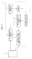
- Fig. 4 is a block diagram showing an example of the conventional structure of the timing generation circuit 4.
- reference numeral 41 is a fast ramp circuit wherein the trigger signal Str is used as a trigger, and the amplified ramp waveforms are output sequentially.
- Reference numeral 42 is a slow ramp circuit comprising a counter 42a that increments the input signals and a D / A conversion circuit that D / A converts and outputs the count value of this counter 42a.
- Reference numeral 43 is a comparator circuit that compares the output of the fast ramp circuit 41 and the output of the slow ramp circuit 42, and outputs the timing signal Stm when they agree. This timing signal Stm becomes the output signal of the timing generation circuit 4. In addition, the timing signal Stm is input into the counter 42a.
- the fast ramp circuit 41 outputs a ramp waveform when the trigger signal Str is input (refer to Fig. 5 (b)).
- the slow ramp circuit 42 when the output of the comparator circuit 43 is input, the counter 42a is incremented by 1, and this count value is made into an analogue value by the D / A conversion circuit 42b, and output.
- a step-shaped waveform is generated (refer to Fig. 5 (c)).
- the comparator circuit 43 compares the output of the fast ramp circuit 41 and the output of the slow ramp circuit 42, and after the trigger signal Str is input and rises to the point they agree the first time, outputs a pulse having a pulse width of a specified time (refer to Fig. 5 (d)). This becomes the timing signal Stm.
- an unnecessary signal (the section shown by reference number S3 in Fig. 2 (d)) is output form the comparator circuit 43 because there is a timing that agrees with the output of the slow ramp circuit 42. Because the output of the comparator circuit 43 is the timing signal Stm, when unstable signals and unnecessary signals are output, there is the problem that accurate sampling cannot be carried out.
- an object of the present invention to provide an EOS oscilloscope that can prevent the output of an unstable output value from the comparator circuit, and can improve the precision of the timing signal.
- this objective can be attained by an electro-optical sampling oscilloscope apparatus that carries out measurement of measured signal by using an optical pulse generated based on a timing signal generated from a timing generation circuit synchronous with a trigger signal, providing the timing generation circuit comprising a fast ramp circuit that outputs a ramp waveform using said trigger signal as a trigger; a slow ramp circuit that increases stepwise and sequentially the output value according to said timing signal; a comparator circuit that compares the output of said fast ramp circuit and the output of said slow ramp circuit and outputs the results of this comparison; and a gate circuit that limits the output of said comparator circuit by closing a gate only when the output of said comparator circuit is unstable based on the input trigger signal and timing signal.
- the present invention provides the advantages that the precision of the timing signal is improved because unnecessary timing signals are not output by receiving an output of the comparator circuit at a gate circuit, and closing the gate during the time that the output of the fast ramp circuit returns from a maximum value to a minimum value and during the time that the D / A conversion operation of the D / A conversion circuit that becomes the output of the slow ramp circuit.
- Fig. 1 is a block diagram showing the structure of an embodiment of the present invention.
- Fig. 2 is a timing diagram of the operation of the slow ramp circuit 42 in the embodiment shown in Fig. 1.
- Fig. 3 is a block diagram showing the structure of an EOS oscilloscope.
- Fig. 4 is a block diagram showing the circuit structure of a conventional example of a timing generation circuit in the EOS oscilloscope.
- Fig. 5 is a timing diagram shown the operation that generates the timing signal in a conventional example shown in Fig. 4.
- the EOS oscilloscope is structured from an EOS oscilloscope main body 1 and an electro-optic probe 2.
- the trigger circuit 3 receives a signal from the outside, and outputs the trigger signal that marks the beginning of the measurement of the measured signal.
- the timing generation circuit 4 generates the generation timing of the optical pulse and the timing for an A / D conversion, and the optical pulse generation circuit 5 carries out the generation of the optical pulse based on the timing signal from the timing generation circuit 4.
- the optical pulse form the optical pulse generation circuit 5 is supplied to the electro-optic probe 2, and is subject to a change in polarization by an electro-optic element.
- the polarization of this polarized optical pulse is detected in the electro-optic probe 2, and converted to an electrical signal.
- This signal is input into the EOS oscilloscope main body 1, amplification of the signal and A / D conversion is carried out by the A / D conversion circuit 6, processing is carried out on the signal which is the object of measurement for displaying, etc., by the processing circuit 7, and it is displayed on a display 8.
- the present invention improves the timing generation circuit 4.
- timing generation circuit 4 in the EOS oscilloscope is explained referring to Fig. 1.
- parts identical to the conventional circuit shown in Fig. 4 have the same reference number, and their explanation is omitted.
- the timing generation circuit shown in this figure differs from the conventional circuit in that a gate circuit 44 is provided.
- This gate circuit 44 is a circuit that limits the output of the timing signal Stm by opening and closing a gate using the trigger signal Str and output of the AND circuit 44c as a trigger.
- the gate circuit 44 comprises a timer 44a that inputs the trigger signal Str and the output of the AND circuit 44c, measures a specific time from the rise of the various input signals, and takes the value "H" (high) only during that time; a NOT circuit 44b that inverts and outputs the output of the timer 44a; and an AND circuit 44c that outputs the logical product of the output of the NOT circuit 44b and the comparator circuit 43.
- the output of the AND circuit 44c becomes the timing signal Stm.
- the fast ramp circuit 41 When the trigger signal Str is output to the fast ramp circuit 41, the fast ramp circuit 41 outputs the ramp waveform.
- This ramp waveform acquires its maximum value after time T3 from the rise of the trigger signal Str, and from this point become a waveform having a minimum value after time T4 (refer to Fig. 2 (b)).
- the slow ramp circuit 42 outputs a step-shaped waveform having an output value that increases each time the timing signal Stm is output.
- This waveform is the value of the count value of the counter 42a that has been D / A converted and output, and during the operation of the D / A conversion, becomes an unstable output (refer to reference numeral S1 of Fig. 2 (c)).
- the comparator circuit 43 compares the output of the fast ramp circuit 41 and the output of the slow ramp circuit 42, and takes the value "H" (high) when they agree.
- the unstable output of the slow ramp circuit 42 is input, and as a result the comparator circuit 43 also has an unstable output fluctuation.
- the output value of the fast ramp circuit 41 intersects the output of the slow ramp circuit 42 when the output of the fast ramp circuit 41 returns to the minimum value, the output of the comparator circuit 43 becomes unstable (refer to Fig. 2 (d)).
- the D / A conversion is in operation and the output of the fast ramp circuit 41 returns to a minimum value.
- the time during which this output is unstable is determined by the time of the D / A conversion of the D / A conversion circuit 42b and the output waveform of the fast ramp circuit 41. If this time is measured by a timer, the gate is closed, and the output value of the comparator circuit 43 is limited, then it is possible to generate a correct timing signal.
- the timer 44a rises at a time T1 after the rise of the timing signal Stm, and from this point, a signal that rises after time T2, during which the output of the D / A conversion circuit is unstable, is output. That is, when the output of the slow ramp circuit 42 is not stable (the section shown by the reference numeral S1 in Fig. 2 (c)), a signal with the value "H" (high) is output (refer to reference number S4 in Fig. 2 (e)).
- the timer 44a outputs a signal that rises after the time T3 from the rise of the trigger signal until the ramp waveform of the fast ramp circuit becomes a maximum value (refer to Fig. 2 (b)) and from this point falls after time T4, until the ramp waveform of the fast ramp circuit 41 becomes a minimum value. That is, in the case that the output of the fast ramp circuit 41 returns to a minimum value from a maximum value, when it agrees with the output of the slow ramp circuit 42 and an unnecessary value is output from the comparator circuit 43 (the section indicated by reference number S3 if Fig. 2 (d)), a signal taking the value "H" (high) is output (refer to reference number S5 in Fig. 2 (e)).
- the output of the timer 44a comprises a signal (reference number S4 is Fig. 2 (e)) taking the value "H" (high) when the output of the slow ramp circuit 42 is unstable and a signal (reference number S5 in Fig. 2 (e)) taking the value "H" (high) when an unnecessary output value is output from the comparator, each generated by the timer, and the their logical sum can be taken.
- the time of the rise and fall of the output of the timer 44a is determined at times T1, T2, T3, and T4, but these can also be arbitrarily set to suit the output waveform of the fast ramp circuit 41 and the D / A converter used by the slow ramp circuit 42.
- the NOT circuit 44b outputs a signal that inverts the output of the timer 44a. That is, it outputs a signal that takes the value "L" (low) only when an unnecessary output value is output from the comparator circuit 43 (refer to Fig. 2 (f)).
- the AND circuit 44c can output a timing signal Stm only when the output of the fast ramp circuit 42 and the output of the slow ramp circuit 42 agree by outputting the logical product of the output of the NOT circuit 44b and the output of the comparator circuit 43 (refer to Fig. 2 (g)).
- a gate circuit 44 is provided, and when an unnecessary output value is output from the comparator circuit 43, a correct timing signal Stm can be obtained because the gate has been closed.
Landscapes
- Physics & Mathematics (AREA)
- General Physics & Mathematics (AREA)
- Tests Of Electronic Circuits (AREA)
- Measurement Of Current Or Voltage (AREA)
- Measurement Of Unknown Time Intervals (AREA)
Applications Claiming Priority (3)
| Application Number | Priority Date | Filing Date | Title |
|---|---|---|---|
| JP10155046A JPH11352156A (ja) | 1998-06-03 | 1998-06-03 | 電気光学サンプリングオシロスコープ |
| JP15504698 | 1998-06-03 | ||
| US09/323,942 US6288529B1 (en) | 1998-06-03 | 1999-06-02 | Timing generation circuit for an electro-optic oscilloscope |
Publications (1)
| Publication Number | Publication Date |
|---|---|
| EP0962782A1 true EP0962782A1 (de) | 1999-12-08 |
Family
ID=26483155
Family Applications (1)
| Application Number | Title | Priority Date | Filing Date |
|---|---|---|---|
| EP99304356A Withdrawn EP0962782A1 (de) | 1998-06-03 | 1999-06-03 | Elektro-optisches Abtast-Oszilloskop |
Country Status (3)
| Country | Link |
|---|---|
| US (1) | US6288529B1 (de) |
| EP (1) | EP0962782A1 (de) |
| JP (1) | JPH11352156A (de) |
Families Citing this family (4)
| Publication number | Priority date | Publication date | Assignee | Title |
|---|---|---|---|---|
| JP2001099717A (ja) * | 1999-09-30 | 2001-04-13 | Ando Electric Co Ltd | 波長計のデータ処理装置、及びそのデータ処理方法 |
| US6711954B2 (en) * | 2001-01-19 | 2004-03-30 | Lockheed Martin Corporation | Method and apparatus for improving the dynamic range of laser detected ultrasound in attenuative materials |
| JP2005249690A (ja) * | 2004-03-05 | 2005-09-15 | Agilent Technol Inc | 信号保持方法、アナログ・ディジタル変換方法、信号保持装置、アナログ・ディジタル変換装置、および、信号観測装置 |
| US7045992B1 (en) * | 2004-06-22 | 2006-05-16 | National Semiconductor Corporation | Apparatus and method for start-up for a synchronous switching regulator |
Citations (2)
| Publication number | Priority date | Publication date | Assignee | Title |
|---|---|---|---|---|
| EP0345011A1 (de) * | 1988-05-30 | 1989-12-06 | Hamamatsu Photonics K.K. | Elektrische Signalüberwachungsvorrichtung |
| JPH0582606A (ja) * | 1991-09-19 | 1993-04-02 | Fujitsu Ltd | 半導体集積回路試験装置 |
Family Cites Families (24)
| Publication number | Priority date | Publication date | Assignee | Title |
|---|---|---|---|---|
| US4219762A (en) * | 1979-01-26 | 1980-08-26 | Gilbert Raine M | Wideband self-calibrated fiber-optic data link with fiber-optic storage |
| JP2598458B2 (ja) * | 1988-05-31 | 1997-04-09 | 浜松ホトニクス株式会社 | 電気信号観測装置 |
| JP2607798B2 (ja) | 1991-03-18 | 1997-05-07 | 日本電信電話株式会社 | 集積回路の電圧信号測定方法および測定装置 |
| JPH04295028A (ja) * | 1991-03-26 | 1992-10-20 | Nippon Sheet Glass Co Ltd | 濃色ガラスおよびその製造法 |
| JP2542754B2 (ja) | 1991-08-05 | 1996-10-09 | 日本電信電話株式会社 | 集積回路の電界測定用プロ―ブ位置決め方法および位置決め装置 |
| JPH0547883A (ja) | 1991-08-12 | 1993-02-26 | Nippon Telegr & Teleph Corp <Ntt> | 集積回路の回路試験装置および回路試験方法 |
| JPH0580083A (ja) | 1991-09-20 | 1993-03-30 | Nippon Telegr & Teleph Corp <Ntt> | 集積回路の試験方法および装置 |
| JP3187505B2 (ja) | 1992-03-02 | 2001-07-11 | 日本電信電話株式会社 | 集積回路の電界測定装置 |
| JP3139644B2 (ja) | 1992-09-11 | 2001-03-05 | 日本電信電話株式会社 | 集積回路の電圧信号測定装置 |
| US5546325A (en) * | 1993-02-04 | 1996-08-13 | International Business Machines Corporation | Automated system, and corresponding method, for testing electro-optic modules |
| JP3165873B2 (ja) | 1993-08-06 | 2001-05-14 | 日本電信電話株式会社 | 電気信号測定方法および装置 |
| JPH0755891A (ja) | 1993-08-09 | 1995-03-03 | Nippon Telegr & Teleph Corp <Ntt> | 集積回路の試験方法および試験装置 |
| US5844288A (en) * | 1994-07-06 | 1998-12-01 | The Regents Of The University Of Michigan | Photoconductive element and method for measuring high frequency signals |
| JPH0843499A (ja) | 1994-08-03 | 1996-02-16 | Nippon Telegr & Teleph Corp <Ntt> | ティップ型回路試験用電界センサおよびその電界検出方法 |
| JP3489701B2 (ja) | 1994-08-04 | 2004-01-26 | 日本電信電話株式会社 | 電気信号測定装置 |
| JPH08152361A (ja) | 1994-11-29 | 1996-06-11 | Nippon Telegr & Teleph Corp <Ntt> | 光信号波形の測定装置 |
| JPH08160110A (ja) | 1994-12-06 | 1996-06-21 | Nippon Telegr & Teleph Corp <Ntt> | 電気信号測定装置 |
| JP3326317B2 (ja) | 1995-12-05 | 2002-09-24 | 横河電機株式会社 | 電圧測定装置 |
| JP3334743B2 (ja) | 1996-01-19 | 2002-10-15 | 日本電信電話株式会社 | 電気信号測定装置 |
| JPH09211035A (ja) | 1996-01-30 | 1997-08-15 | Nippon Telegr & Teleph Corp <Ntt> | 電界測定装置 |
| JP3352376B2 (ja) * | 1997-12-15 | 2002-12-03 | 安藤電気株式会社 | 電気光学サンプリングオシロスコープ |
| JP3372468B2 (ja) * | 1998-01-13 | 2003-02-04 | 安藤電気株式会社 | 電気光学サンプリングオシロスコープ |
| JP3372467B2 (ja) * | 1998-01-13 | 2003-02-04 | 安藤電気株式会社 | 電気光学サンプリングオシロスコープ |
| JP3377943B2 (ja) * | 1998-01-13 | 2003-02-17 | 安藤電気株式会社 | 電気光学サンプリングオシロスコープ |
-
1998
- 1998-06-03 JP JP10155046A patent/JPH11352156A/ja active Pending
-
1999
- 1999-06-02 US US09/323,942 patent/US6288529B1/en not_active Expired - Fee Related
- 1999-06-03 EP EP99304356A patent/EP0962782A1/de not_active Withdrawn
Patent Citations (2)
| Publication number | Priority date | Publication date | Assignee | Title |
|---|---|---|---|---|
| EP0345011A1 (de) * | 1988-05-30 | 1989-12-06 | Hamamatsu Photonics K.K. | Elektrische Signalüberwachungsvorrichtung |
| JPH0582606A (ja) * | 1991-09-19 | 1993-04-02 | Fujitsu Ltd | 半導体集積回路試験装置 |
Non-Patent Citations (1)
| Title |
|---|
| PATENT ABSTRACTS OF JAPAN vol. 017, no. 415 (E - 1407) 3 August 1993 (1993-08-03) * |
Also Published As
| Publication number | Publication date |
|---|---|
| US6288529B1 (en) | 2001-09-11 |
| JPH11352156A (ja) | 1999-12-24 |
Similar Documents
| Publication | Publication Date | Title |
|---|---|---|
| US5712582A (en) | Test signal generator having timing calibration circuit | |
| JPH0447269B2 (de) | ||
| JPWO2001020288A1 (ja) | オプチカルタイムドメインリフレクトメータ | |
| EP0962782A1 (de) | Elektro-optisches Abtast-Oszilloskop | |
| US6839130B2 (en) | Optical fiber measuring apparatus | |
| US7046094B2 (en) | Method and ring oscillator circuit for measuring circuit delays over a wide operating range | |
| US4105932A (en) | "Slewed pulse" scope sweep calibrator | |
| US6232765B1 (en) | Electro-optical oscilloscope with improved sampling | |
| US2939075A (en) | Delay calibrating apparatus | |
| EP0921402A2 (de) | Elektro-optisches Abtast-oszilloskop | |
| EP0908732A2 (de) | Elektrooptisches Sampling-Oszilloskop | |
| US6377036B1 (en) | Electro-optic sampling oscilloscope | |
| JP3379905B2 (ja) | 電気光学サンプリングオシロスコープ | |
| PL175439B1 (pl) | Sposób mierzenia interwału czasowego i urządzenie do mierzenia interwału czasowego | |
| JP3101101B2 (ja) | パルスパワーメータ | |
| RU2100815C1 (ru) | Устройство для регистрации формы однократных оптических и электрических импульсных сигналов | |
| RU2043637C1 (ru) | Осциллограф | |
| EP0918225A2 (de) | Elektrooptisches Sampling-Oszilloskop | |
| RU2159446C1 (ru) | Способ калибровки стробоскопических преобразователей | |
| US6654700B2 (en) | Testing method of semiconductor integrated circuit and equipment thereof | |
| JP3080480B2 (ja) | 信号遅延時間測定装置 | |
| RU2106646C1 (ru) | Осциллограф | |
| JPH08223006A (ja) | 遅延時間調整方法及び遅延時間調整装置 | |
| SU1711234A2 (ru) | Измеритель параметров аналогового запоминающего устройства | |
| JPS60113161A (ja) | 出力波形の計測調整装置 |
Legal Events
| Date | Code | Title | Description |
|---|---|---|---|
| PUAI | Public reference made under article 153(3) epc to a published international application that has entered the european phase |
Free format text: ORIGINAL CODE: 0009012 |
|
| AK | Designated contracting states |
Kind code of ref document: A1 Designated state(s): DE GB |
|
| AX | Request for extension of the european patent |
Free format text: AL;LT;LV;MK;RO;SI |
|
| 17P | Request for examination filed |
Effective date: 20000112 |
|
| RIN1 | Information on inventor provided before grant (corrected) |
Inventor name: YAMADA, JUNZO C/O NIPPON TELEGRAPH AND Inventor name: NAGATSUMA, TADAO C/O NIPPON TELEGRAPH AND Inventor name: SHINAGAWA, MITSURU C/O NIPPON TELEGRAPH. AND Inventor name: ENDOU, YOSHIO C/O ANDO ELECT. CO.,LTD, Inventor name: BANJOU, NOBUKAZU C/O ANDO ELECT. CO.,LTD, Inventor name: KIKUCHI JUN C/O ANDO ELECT. CO.,LTD, Inventor name: YANAGISAWA, YOSHIKI, C/O ANDO ELECT. CO.,LTD, Inventor name: TAKEUCHI, NOBUAKI C/O ANDO ELECTRIC CO., LTD, |
|
| AKX | Designation fees paid |
Free format text: DE GB |
|
| 17Q | First examination report despatched |
Effective date: 20030901 |
|
| STAA | Information on the status of an ep patent application or granted ep patent |
Free format text: STATUS: THE APPLICATION IS DEEMED TO BE WITHDRAWN |
|
| 18D | Application deemed to be withdrawn |
Effective date: 20040101 |