EP0918225A2 - Elektrooptisches Sampling-Oszilloskop - Google Patents
Elektrooptisches Sampling-Oszilloskop Download PDFInfo
- Publication number
- EP0918225A2 EP0918225A2 EP98309261A EP98309261A EP0918225A2 EP 0918225 A2 EP0918225 A2 EP 0918225A2 EP 98309261 A EP98309261 A EP 98309261A EP 98309261 A EP98309261 A EP 98309261A EP 0918225 A2 EP0918225 A2 EP 0918225A2
- Authority
- EP
- European Patent Office
- Prior art keywords
- circuit
- signal
- pulse
- electro
- sampling
- Prior art date
- Legal status (The legal status is an assumption and is not a legal conclusion. Google has not performed a legal analysis and makes no representation as to the accuracy of the status listed.)
- Withdrawn
Links
Images



Classifications
-
- G—PHYSICS
- G01—MEASURING; TESTING
- G01R—MEASURING ELECTRIC VARIABLES; MEASURING MAGNETIC VARIABLES
- G01R13/00—Arrangements for displaying electric variables or waveforms
- G01R13/02—Arrangements for displaying electric variables or waveforms for displaying measured electric variables in digital form
- G01R13/0281—Arrangements for displaying electric variables or waveforms for displaying measured electric variables in digital form using electro-optic elements
Definitions
- the present invention relates to an electro-optic sampling oscilloscope which measures a measurement signal to be measured using optical pulses generated based on a signal from a pulse circuit which pulses sampling signals and, in particular, to an electro-optic sampling oscilloscope characterized by a pulse circuit for the purpose of pulsing the sampling signal.
- EOS electro-optic sampling oscilloscope
- the EOS oscilloscope comprises an EOS oscilloscope main body 1 and an electro-optic probe 2.
- the trigger circuit 3 is a circuit related to the trigger signal which initiates measurement of the signal to be measured.
- delay circuit 4 delays the signal from the trigger circuit 3 by only a delay time set for the purpose of conversion of the starting position of the sampling.
- Sweep circuit 5 uses the signal from delay circuit 4 as an input signal and generates a sampling signal for sampling, and this sampling signal is pulsed by pulse circuit 6.
- optical pulse generation circuit 7 generates optical pulses.
- the optical pulses from this optical pulse generation circuit 7 are supplied to the electro-optic probe 2 and undergo polarity conversion by an electro-optic element.
- the optical pulses which has undergone this polarization change undergo polarization detection by a polarization detection optical system (not shown in the Figure) in the electro-optic probe 2, and this signal is input into the EOS oscilloscope main body 1.
- the signals from the electro-optic probe 2 undergo signal amplification and A/D conversion by the A/D conversion circuit 8.
- the processing circuit 9, which comprises a CPU (central processing unit) and the like, carries out the processing for the purpose of displaying the signal that is the subject of measurement.
- the delay circuit 4 outputs a signal delayed by a predetermined time only (in the Example in part (b) in the Figure, this is time T).
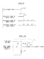
- the sweep circuit 5 outputs a sampling signal for the purpose of sampling based on the output signal from the delay circuit 4 as shown in part (c) in Figure 9.
- the pulse circuit 6 pulses the signal from sweep circuit 5 as in part (d) in Figure 9.
- FIG 10 is a diagram of a conventional example of pulse circuit 6.
- the pulse circuit 6 comprises two step recovery diodes (hereinafter abbreviated as "SRD") 21 and 22, two condensers 23 and 24, and two resistors 25 and 26.
- SRD step recovery diodes
- a fixed bias voltage is supplied through the resistor 25 and resistor 26 as the bias voltage of the SRD 21 and the SRD 22. Then, the pulse circuit 6 outputs a pulsed signal from the SRD 22.
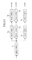
- FIG. 11 is a diagram showing a part of the inside of an EOS oscilloscope main body 1.
- FIG. 11 there are from 1 to n channels, and as shown by reference symbols 6a to 6n, there are n number of pulse circuits provided.
- delay circuits 15a ⁇ 15n are provided, and adjustment of the skew of each of these channels is carried out by these delay circuits 15a ⁇ 15n.
- the present invention was made in view of these circumstances and the object of the present invention is to provide an electro-optic sampling oscilloscope in which delay processing is also possible in the pulse circuit and, thereby, the circuit structure can be simplified.
- the present invention provides an electro-optic sampling oscilloscope for conducting measurement of a signal to be measured using an optical pulse generated based on a signal from a pulse circuit which pulses sampling signals.
- the pulse circuit comprises a step recovery diode, and the bias voltage of said step recovery diode is variable.
- the delay circuit when the delay processing is within the range which can be carried out by the pulse circuit, the delay circuit can be omitted, and it is possible to simplify the circuit structure. Moreover, when the delay circuit is omitted, the effect that unstable factors such as jitter are not present results.
- the present invention provides an electro-optic sampling oscilloscope for conducting measurement of a signal to be measured for each channel using an optical pulse generated based on signals from a pulse circuit provided in each channel for the purpose of pulsing sampling signals.
- the pulse circuit comprises a step recovery diode and the bias voltage of said step recovery diode is variable.
- a pulse circuit is provide for each channel, and it is possible to carry out time delay by varying the bias voltage of the step recovery diode which is contained in this pulse circuit.
- this pulse circuit it is also possible to adjust the skew of each channel and, thereby, it is not necessary to provide a delay circuit for each channel.
- Figure 1 is a structural diagram is a delay pulse circuit of an EOS oscilloscope according to an embodiment of the present invention.
- FIG. 2 is a diagram showing the structure of an EOS oscilloscope according to an embodiment of the present invention.
- Figure 3 is a circuit diagram according to an embodiment of the pulse circuit.
- Figure 4 is a timing chart for the purpose of explaining the relationship between the output signal from the sweep circuit and the output signal from the delay pulse circuit.
- Figure 5 is a diagram showing the relationship between the bias voltage and the delay time in a given step recovery diode.
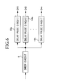
- Figure 6 is a diagram showing the structure between a delay pulse circuit and a sweep circuit when there are a plurality of channels in an EOS oscilloscope according to an embodiment of the present invention.
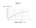
- Figure 7 is a Figure showing a relationship between a delay time and a forward current in a given step recovery diode.
- Figure 8 is a diagram showing the structure of an example of a conventional EOS oscilloscope.
- Figure 9 is a timing chart for the purpose of explaining the operation of the EOS oscilloscope shown in Figure 8.
- Figure 10 is a circuit diagram according to a conventional example of a pulse circuit.
- Figure 11 is a diagram showing a conventional example of the structure between a pulse circuit and a sweep circuit when there are a plurality of channels in an EOS oscilloscope.
- the EOS oscilloscope comprises an EOS oscilloscope main body 1 and an electro-optic probe 2.
- the EOS oscilloscope main body 1 comprises a trigger circuit 3, delay circuit 4, a sweep circuit 5, a delay pulse circuit 10, an optical pulse generation circuit 7, an A/D conversion circuit 8, and a processing circuit 9.
- trigger circuit 3 is a circuit related to trigger signals which initiate measurement with respect to measurement signals.
- delay circuit 4 delays the signal from the trigger signal 3 by only the delay time set for the purpose of changing the initial position of the sampling of the signal to be measured.
- the sweep circuit 5 generates a sampling signal for sampling, based on the signal from delay circuit 4.
- Delay pulse circuit 10 uses, as input signals, sampling signals from the sweep circuit 5 and control signals from the processing circuit 9 which comprises a CPU (central processing unit) and the like.
- the delay pulse circuit 10 delays a sampling signal based on the control signal from processing circuit 9, pulses the sampling signal and outputs delayed and pulsed signal.
- the reason why it is necessary for pulsing is because the width of the sampling signal from the sweep circuit 5 is too large to be used as a signal for outputting optical pulses from optical pulse generation circuit 7.
- the optical pulse generation circuit 7 generates optical pulses based these pulsed signals.
- the optical pulses from the optical pulse generation circuit 7 are supplied to the electro-optic probe 2 and undergo polarization change by an electro-optic element.
- the optical pulses which have undergone this polarization change are detected by a polarization detection system (not shown in the Figures), and these signals are input into the EOS oscilloscope main body 1.
- the signal from the electro-optic probe 2 undergoes signal amplification and A/D conversion by the A/D conversion circuit 8.
- the processing circuit 9 carries out the processing for the purpose of displaying the signal which is the subject of measurement.
- the delay pulse circuit 10 it is also possible for the delay pulse circuit 10 to carry out delay processing of the signal of the sweep circuit 5 within a certain time range. Therefore, when the necessary time delay is within the range which can be delayed by the delay pulse circuit 10, it is possible to omit the delay circuit 4.
- EOS oscilloscope when called an "EOS oscilloscope", there are situations in which this comprises the EOS oscilloscope main body 1 and the electro-optic probe 2 of Figure 1, and situations in which there is only the EOS oscilloscope main body 1.
- FIG. 1 is a diagram showing the structure of a delay pulse circuit 10 in an EOS oscilloscope.
- delay pulse circuit 10 comprises a pulse circuit 11 and a D/A conversion circuit 12.
- the information ⁇ T which relates to the delay time from processing circuit 9 and the sampling signal from sweep circuit 5 is used as an input signal, the delay pulse circuit 10 outputs signal which is the delayed by ⁇ T and pulsed sampling signal.
- the D/A conversion circuit 12 is provided for the conversion of digital information ⁇ T related to the delay time from the processing circuit 9 into an analogue signal.
- the pulse circuit 11 has a structure which includes an SRD. This SRD has the characteristic of generating delays in accordance with bias voltage.
- the signal from the D/A conversion circuit 12 is input as bias voltage of SRD, and the pulse circuit 11 carries out the delay in accordance with the bias voltage and with respect to the sampling signal from the sweep circuit 5, pulses the sampling signal, and outputs the delayed and pulsed signal.
- FIG 3 is a diagram showing an example of the circuit structure of a pulse circuit 11.
- the pulse circuit 11 comprises two SRDs 41 and 42, a condenser 43, two resistors 44 and 45, and transistors TR1 and TR2.
- the bias voltage which is the output from the D/A converter 12 is input to the base of the bias setting transistor TR2, and controls the source voltage of the transistor TR1 for amplifying the sampling signal from sweep circuit 5.
- the pulse output section which comprises SRD 41 and 42 and condenser 43
- the bias voltage from the D/A converter 12 and the pulse from the sweep circuit 5 are supplied as a single signal.
- the pulse output section delays the sampling signal in accordance with the bias voltage and pulses the sampling signal. And the delayed and pulsed signal is output from the SRD 42.
- SRD has temperature characteristics
- a circuit (not shown in the Figures) is necessary for maintaining the temperature of these SRDs 41 and 42 within a specified range.
- SRDs 41 and 42 one input signal is sufficient, and SRD 41 and 42 can be arranged adjacently, and it is possible to shorten the connection electrical wiring for the purpose of temperature control.
- the connection electrical wiring When it is possible to shorten the connection electrical wiring, the dispersion of heat by the electrical wiring can be reduced and stable temperature control is easy.
- the delay pulse circuit 10 carries out delay of delay time ⁇ T which is set by processing circuit 9 and outputs the delayed and pulsed sampling signal as shown in part (b) in Figure 4.
- the pulsed signal having a width of 200 [ps] is generated.
- the processing circuit 9 stores information with regard to the relationship between the bias voltage and the delay time of the SRD which is comprised by pulse circuit 11 such as shown in Figure 5, for example, and, based on this information, determines a bias voltage which corresponds to the desired delay time, and outputs it to the D/A conversion circuit 12 as a digital signal.
- the desired delay time is established by a user of the EOS oscilloscope via a setting section, not shown in the Figures, for the purpose of changing the initial measurement position of the signal to be measured. In the example of Figure 5, delay processing at a range of 0 ⁇ 500 [ps] is possible.
- delay processing is made possible by variation ofthe bias voltage for pulse circuit 11. Therefore, when the delay processing is within the range which can be conducted by the pulse circuit 11, delay circuit 4 can be omitted, and it is possible to carry out simplification of the circuit structure. Moreover, when the delay processing exceeds the range which can be conducted by the pulse circuit 11, it is possible to conduct delay processing by combination with a delay circuit 4.
- the delay pulse circuit 10 shown in Figure 1 may be provided for each channel as shown by references 10a to 10n in Figure 6. Since the delay pulse circuits 10a ⁇ 10n can also carry out delay processing, based on this, it is not necessary to provide a delay circuit for each channel for the purpose of adjusting skew.
- Figure 6 is a diagram showing a part of the inside of the EOS oscilloscope main body 1. It is possible for the bias voltage to be varied and then input to each delay pulse circuit 10a ⁇ 10n, for the purpose of adjusting the skew of each channel by signal wires which are not shown in the Figure.
- the processing circuit 7 stores information regarding the relationship between the forward current and the delay time of the SRD which is comprised by pulse circuit 11 such as shown in Figure 7, and based on this information, the current for the desired delay time is determined and is output to the D/A conversion circuit 12.
- a pulse circuit is provided in the EOS oscilloscope for the purpose of pulsing sampling signals.
- This pulse circuit has a step recovery diode as a component, the bias voltage of this step recovery diode is variable, and, thereby, delay processing can carried out.
- the delay circuit can be omitted, and it is possible to simplify the circuit structure.
- the delay circuit is omitted, the effect that unstable factors such as jitter are not present results.
- a pulse circuit is provide for each channel, and it is possible to carry out time delay by varying the bias voltage of the step recovery diode which is contained in this pulse circuit.
- this pulse circuit it is also possible to adjust the skew of each channel and, thereby, it is not necessary to provide a delay circuit for each channel.
- a D/A conversion circuit is provided for the purpose of supplying bias voltage to the step recovery diode which makes up the pulse circuit. By this, it is possible to control the delay time from the processing circuit which comprises the CPU, and the like, via the D/A conversion circuit.
Landscapes
- Physics & Mathematics (AREA)
- General Physics & Mathematics (AREA)
- Measurement Of Current Or Voltage (AREA)
- Tests Of Electronic Circuits (AREA)
Applications Claiming Priority (3)
| Application Number | Priority Date | Filing Date | Title |
|---|---|---|---|
| JP31869997A JP3406499B2 (ja) | 1997-11-19 | 1997-11-19 | 電気光学サンプリングオシロスコープ |
| JP31869997 | 1997-11-19 | ||
| JP318699/97 | 1997-11-19 |
Publications (2)
| Publication Number | Publication Date |
|---|---|
| EP0918225A2 true EP0918225A2 (de) | 1999-05-26 |
| EP0918225A3 EP0918225A3 (de) | 2000-08-23 |
Family
ID=18102023
Family Applications (1)
| Application Number | Title | Priority Date | Filing Date |
|---|---|---|---|
| EP98309261A Withdrawn EP0918225A3 (de) | 1997-11-19 | 1998-11-12 | Elektrooptisches Sampling-Oszilloskop |
Country Status (2)
| Country | Link |
|---|---|
| EP (1) | EP0918225A3 (de) |
| JP (1) | JP3406499B2 (de) |
Cited By (3)
| Publication number | Priority date | Publication date | Assignee | Title |
|---|---|---|---|---|
| CN104374973A (zh) * | 2014-11-25 | 2015-02-25 | 苏州立瓷电子技术有限公司 | 一种基于简易前置放大电路的示波器 |
| CN104374975A (zh) * | 2014-11-25 | 2015-02-25 | 苏州立瓷电子技术有限公司 | 一种基于低功耗双重放大电路的示波器 |
| CN104391149A (zh) * | 2014-11-25 | 2015-03-04 | 苏州立瓷电子技术有限公司 | 一种采用分段放大电路的示波器 |
Family Cites Families (10)
| Publication number | Priority date | Publication date | Assignee | Title |
|---|---|---|---|---|
| JPS5139068B1 (de) * | 1968-09-20 | 1976-10-26 | ||
| JPS57118428A (en) * | 1981-01-14 | 1982-07-23 | Yokogawa Hewlett Packard Ltd | Pulse generating circuit |
| US4727340A (en) * | 1986-04-30 | 1988-02-23 | Tektronix, Inc. | Comb generators |
| JP2564148B2 (ja) * | 1987-10-13 | 1996-12-18 | 浜松ホトニクス株式会社 | 電圧検出装置 |
| JPH0666498B2 (ja) * | 1988-05-07 | 1994-08-24 | 浜松ホトニクス株式会社 | 光源駆動装置 |
| JPH07109911B2 (ja) * | 1989-06-16 | 1995-11-22 | 浜松ホトニクス株式会社 | 光源駆動装置 |
| US5179565A (en) * | 1990-06-07 | 1993-01-12 | Hamamatsu Photonics, K.K. | Low noise pulsed light source utilizing laser diode and voltage detector device utilizing same low noise pulsed light source |
| JP2906633B2 (ja) * | 1990-10-12 | 1999-06-21 | 横河電機株式会社 | 光サンプリング装置 |
| JPH08116244A (ja) * | 1994-10-19 | 1996-05-07 | Yokogawa Electric Corp | サンプリング信号発生回路 |
| JP3473925B2 (ja) * | 1995-08-10 | 2003-12-08 | 浜松ホトニクス株式会社 | トリガ回路および電界測定装置 |
-
1997
- 1997-11-19 JP JP31869997A patent/JP3406499B2/ja not_active Expired - Fee Related
-
1998
- 1998-11-12 EP EP98309261A patent/EP0918225A3/de not_active Withdrawn
Cited By (3)
| Publication number | Priority date | Publication date | Assignee | Title |
|---|---|---|---|---|
| CN104374973A (zh) * | 2014-11-25 | 2015-02-25 | 苏州立瓷电子技术有限公司 | 一种基于简易前置放大电路的示波器 |
| CN104374975A (zh) * | 2014-11-25 | 2015-02-25 | 苏州立瓷电子技术有限公司 | 一种基于低功耗双重放大电路的示波器 |
| CN104391149A (zh) * | 2014-11-25 | 2015-03-04 | 苏州立瓷电子技术有限公司 | 一种采用分段放大电路的示波器 |
Also Published As
| Publication number | Publication date |
|---|---|
| JPH11153626A (ja) | 1999-06-08 |
| EP0918225A3 (de) | 2000-08-23 |
| JP3406499B2 (ja) | 2003-05-12 |
Similar Documents
| Publication | Publication Date | Title |
|---|---|---|
| EP1529327B1 (de) | Vorrichtung und verfahren zur messung dynamischer lasersignale | |
| US20070159186A1 (en) | Transmission line pulse measurement system for measuring the response of a device under test | |
| JPS6030898B2 (ja) | ロジツク・アナライザの入力装置 | |
| US6586953B1 (en) | Optically driven driver, optical output type voltage sensor, and IC testing equipment using these devices | |
| CN114089319B (zh) | 一种vcsel器件的纳秒级liv测试系统及方法 | |
| US20180109073A1 (en) | Light-emitting device and distance measurement device | |
| JP2004028983A (ja) | 測定機器及び測定方法 | |
| JP3406499B2 (ja) | 電気光学サンプリングオシロスコープ | |
| US5399978A (en) | Probe apparatus and method for measuring high-frequency signals | |
| US3459969A (en) | System for producing equal and opposite pulses on selected channels | |
| US5185635A (en) | Method of calibrating and controlling the optical power output of an OTDR | |
| US5847570A (en) | Low jitter trigger circuit for electro-optic probing apparatus | |
| EP0921402A2 (de) | Elektro-optisches Abtast-oszilloskop | |
| US8059967B2 (en) | Optical pulse generator and optical pulse tester | |
| US7705622B1 (en) | Method to synchronize two different pulse generators | |
| US4289399A (en) | Light signal observation device | |
| EP0962782A1 (de) | Elektro-optisches Abtast-Oszilloskop | |
| JP2007096100A (ja) | 半導体レーザ駆動用電気パルス発生装置 | |
| CN201616814U (zh) | 超快边沿阶跃脉冲发生器 | |
| US5142284A (en) | Sample and hold with intermediate reset voltage outside of the magnitude range of the input | |
| US6795787B2 (en) | Method and apparatus for calibrating a sampling circuit | |
| US6737853B2 (en) | Photoconductive-sampling voltage measurement | |
| JP3734877B2 (ja) | Ic試験装置のi/o切換スイッチ回路 | |
| JP3001015B2 (ja) | 半導体デバイスドライバ回路 | |
| EP0908734A2 (de) | Elektrooptisches Sampling-Oszilloskop |
Legal Events
| Date | Code | Title | Description |
|---|---|---|---|
| PUAI | Public reference made under article 153(3) epc to a published international application that has entered the european phase |
Free format text: ORIGINAL CODE: 0009012 |
|
| AK | Designated contracting states |
Kind code of ref document: A2 Designated state(s): DE FR GB |
|
| AX | Request for extension of the european patent |
Free format text: AL;LT;LV;MK;RO;SI |
|
| RIN1 | Information on inventor provided before grant (corrected) |
Inventor name: YAMADA, JUNZO, NIPPON TELEGR. & TEL. CORP. Inventor name: NAGATSUMA, TADAO, NIPPON TELEGR. & TEL. CORP. Inventor name: SHINAGAWA, MITSURU, NIPPON TELEGR. & TEL. CORP. Inventor name: ENDOU, YOSHIO, C/O ANDO ELECTRIC CO. LTD. Inventor name: BANJOU, NOBUKAZU, C/O ANDO ELECTRIC CO. LTD. Inventor name: KIKUCHI, JUN, C/O ANDO ELECTRIC CO. LTD. Inventor name: YANAGISAWA, YOSHIKI, C/O ANDO ELECTRIC CO. LTD. Inventor name: TAKEUCHI, NOBUAKI, C/O ANDO ELECTRIC CO. LTD. |
|
| PUAL | Search report despatched |
Free format text: ORIGINAL CODE: 0009013 |
|
| AK | Designated contracting states |
Kind code of ref document: A3 Designated state(s): AT BE CH CY DE DK ES FI FR GB GR IE IT LI LU MC NL PT SE |
|
| AX | Request for extension of the european patent |
Free format text: AL;LT;LV;MK;RO;SI |
|
| 17P | Request for examination filed |
Effective date: 20001128 |
|
| AKX | Designation fees paid |
Free format text: DE FR GB |
|
| RAP1 | Party data changed (applicant data changed or rights of an application transferred) |
Owner name: NIPPON TELEGRAPH ANDTELEPHONE CORPORATION Owner name: YOKOGAWA ELECTRIC CORPORATION |
|
| STAA | Information on the status of an ep patent application or granted ep patent |
Free format text: STATUS: THE APPLICATION IS DEEMED TO BE WITHDRAWN |
|
| 18D | Application deemed to be withdrawn |
Effective date: 20060601 |