EP0962974A2 - Dispositif semi-conducteur - Google Patents
Dispositif semi-conducteur Download PDFInfo
- Publication number
- EP0962974A2 EP0962974A2 EP99303988A EP99303988A EP0962974A2 EP 0962974 A2 EP0962974 A2 EP 0962974A2 EP 99303988 A EP99303988 A EP 99303988A EP 99303988 A EP99303988 A EP 99303988A EP 0962974 A2 EP0962974 A2 EP 0962974A2
- Authority
- EP
- European Patent Office
- Prior art keywords
- resin
- insulating
- semiconductor device
- substrate
- base plate
- Prior art date
- Legal status (The legal status is an assumption and is not a legal conclusion. Google has not performed a legal analysis and makes no representation as to the accuracy of the status listed.)
- Granted
Links
Images




Classifications
-
- H—ELECTRICITY
- H10—SEMICONDUCTOR DEVICES; ELECTRIC SOLID-STATE DEVICES NOT OTHERWISE PROVIDED FOR
- H10W—GENERIC PACKAGES, INTERCONNECTIONS, CONNECTORS OR OTHER CONSTRUCTIONAL DETAILS OF DEVICES COVERED BY CLASS H10
- H10W76/00—Containers; Fillings or auxiliary members therefor; Seals
- H10W76/40—Fillings or auxiliary members in containers, e.g. centering rings
- H10W76/42—Fillings
- H10W76/47—Solid or gel fillings
-
- H—ELECTRICITY
- H10—SEMICONDUCTOR DEVICES; ELECTRIC SOLID-STATE DEVICES NOT OTHERWISE PROVIDED FOR
- H10W—GENERIC PACKAGES, INTERCONNECTIONS, CONNECTORS OR OTHER CONSTRUCTIONAL DETAILS OF DEVICES COVERED BY CLASS H10
- H10W70/00—Package substrates; Interposers; Redistribution layers [RDL]
- H10W70/60—Insulating or insulated package substrates; Interposers; Redistribution layers
- H10W70/67—Insulating or insulated package substrates; Interposers; Redistribution layers characterised by their insulating layers or insulating parts
- H10W70/69—Insulating materials thereof
-
- H—ELECTRICITY
- H10—SEMICONDUCTOR DEVICES; ELECTRIC SOLID-STATE DEVICES NOT OTHERWISE PROVIDED FOR
- H10W—GENERIC PACKAGES, INTERCONNECTIONS, CONNECTORS OR OTHER CONSTRUCTIONAL DETAILS OF DEVICES COVERED BY CLASS H10
- H10W90/00—Package configurations
-
- H—ELECTRICITY
- H10—SEMICONDUCTOR DEVICES; ELECTRIC SOLID-STATE DEVICES NOT OTHERWISE PROVIDED FOR
- H10W—GENERIC PACKAGES, INTERCONNECTIONS, CONNECTORS OR OTHER CONSTRUCTIONAL DETAILS OF DEVICES COVERED BY CLASS H10
- H10W72/00—Interconnections or connectors in packages
- H10W72/50—Bond wires
- H10W72/541—Dispositions of bond wires
- H10W72/547—Dispositions of multiple bond wires
- H10W72/5473—Dispositions of multiple bond wires multiple bond wires connected to a common bond pad
-
- H—ELECTRICITY
- H10—SEMICONDUCTOR DEVICES; ELECTRIC SOLID-STATE DEVICES NOT OTHERWISE PROVIDED FOR
- H10W—GENERIC PACKAGES, INTERCONNECTIONS, CONNECTORS OR OTHER CONSTRUCTIONAL DETAILS OF DEVICES COVERED BY CLASS H10
- H10W72/00—Interconnections or connectors in packages
- H10W72/50—Bond wires
- H10W72/541—Dispositions of bond wires
- H10W72/547—Dispositions of multiple bond wires
- H10W72/5475—Dispositions of multiple bond wires multiple bond wires connected to common bond pads at both ends of the wires
-
- H—ELECTRICITY
- H10—SEMICONDUCTOR DEVICES; ELECTRIC SOLID-STATE DEVICES NOT OTHERWISE PROVIDED FOR
- H10W—GENERIC PACKAGES, INTERCONNECTIONS, CONNECTORS OR OTHER CONSTRUCTIONAL DETAILS OF DEVICES COVERED BY CLASS H10
- H10W72/00—Interconnections or connectors in packages
- H10W72/50—Bond wires
- H10W72/551—Materials of bond wires
- H10W72/552—Materials of bond wires comprising metals or metalloids, e.g. silver
- H10W72/5524—Materials of bond wires comprising metals or metalloids, e.g. silver comprising aluminium [Al]
-
- H—ELECTRICITY
- H10—SEMICONDUCTOR DEVICES; ELECTRIC SOLID-STATE DEVICES NOT OTHERWISE PROVIDED FOR
- H10W—GENERIC PACKAGES, INTERCONNECTIONS, CONNECTORS OR OTHER CONSTRUCTIONAL DETAILS OF DEVICES COVERED BY CLASS H10
- H10W72/00—Interconnections or connectors in packages
- H10W72/851—Dispositions of multiple connectors or interconnections
- H10W72/874—On different surfaces
- H10W72/884—Die-attach connectors and bond wires
-
- H—ELECTRICITY
- H10—SEMICONDUCTOR DEVICES; ELECTRIC SOLID-STATE DEVICES NOT OTHERWISE PROVIDED FOR
- H10W—GENERIC PACKAGES, INTERCONNECTIONS, CONNECTORS OR OTHER CONSTRUCTIONAL DETAILS OF DEVICES COVERED BY CLASS H10
- H10W74/00—Encapsulations, e.g. protective coatings
-
- H—ELECTRICITY
- H10—SEMICONDUCTOR DEVICES; ELECTRIC SOLID-STATE DEVICES NOT OTHERWISE PROVIDED FOR
- H10W—GENERIC PACKAGES, INTERCONNECTIONS, CONNECTORS OR OTHER CONSTRUCTIONAL DETAILS OF DEVICES COVERED BY CLASS H10
- H10W90/00—Package configurations
- H10W90/701—Package configurations characterised by the relative positions of pads or connectors relative to package parts
- H10W90/731—Package configurations characterised by the relative positions of pads or connectors relative to package parts of die-attach connectors
- H10W90/734—Package configurations characterised by the relative positions of pads or connectors relative to package parts of die-attach connectors between a chip and a stacked insulating package substrate, interposer or RDL
-
- H—ELECTRICITY
- H10—SEMICONDUCTOR DEVICES; ELECTRIC SOLID-STATE DEVICES NOT OTHERWISE PROVIDED FOR
- H10W—GENERIC PACKAGES, INTERCONNECTIONS, CONNECTORS OR OTHER CONSTRUCTIONAL DETAILS OF DEVICES COVERED BY CLASS H10
- H10W90/00—Package configurations
- H10W90/701—Package configurations characterised by the relative positions of pads or connectors relative to package parts
- H10W90/751—Package configurations characterised by the relative positions of pads or connectors relative to package parts of bond wires
- H10W90/754—Package configurations characterised by the relative positions of pads or connectors relative to package parts of bond wires between a chip and a stacked insulating package substrate, interposer or RDL
Definitions
- the present invention relates to a semiconductor device in which a case of the semiconductor device contains semiconductor elements and is filed with resin.
- a power semiconductor device is disclosed in Japanese Patent Application Laid-Open Hei 8-125071.
- Fig. 10 shows a cross-sectional view showing the schematic composition of the conventional power semiconductor device.
- a ceramic substrate 3a, on whose top and back surfaces copper sheets 3b are attached, is soldered to a metal base plate 1, and a leader-line terminal is led out from the copper sheet 3b attached on the top surface of the ceramic substrate 3a.
- the peripheral part of the ceramic substrate (insulating substrate) 3a is covered with silicone rubber adhesive 14, and the insulating substrate 3a is contained in a case 6, and is covered with gel silicone rubber 5b poured into the case 6.
- a space among a terminal block 8, the gel silicone rubber 5b, and the case 6 is sealed with epoxy resin 15.
- the silicone rubber adhesive 14 covering the peripheral part of the ceramic substrate 3a prevents the decrease of the creepage withstand voltage of the substrate 3a.
- the subjects in the conventional semiconductor device are as follows.
- expansion and contraction of the silicone rubber adhesive 14, which is shown by the arrow mark 17, may bend and break the peripheral part of the ceramic substrate 3a. If the ceramic substrate 3a is broken, the creepage distance between the base plate 1 and the copper sheet attached on the surface of the ceramic substrate 3a decreases, which degrades the withstand voltage of the semiconductor device.
- the present invention has been achieved in consideration of the above descried subjects, and is aimed at providing a semiconductor device with a high reliability, in which the withstand voltage hardly deteriorates.
- the present invention provides a semiconductor device including a base plate and at least one insulating substrate with at least one conductive plate attached on the top surface of the insulating substrate mounted on the base plate, whose back surface facing the base plate.
- the base plate is contained in a case, and semiconductor elements are arranged in the case.
- the case is filled with a first resin.
- the surface region of the insulating substrate, between the edge part of the conductive plate and the peripheral part of the insulating substrate is covered with a second resin. Further, the edges of the second resin exist between the edge part of the conductive plate and the peripheral part of the insulating substrate.
- the second resin since the edges of the second resin exist between the edge part of the conductive plate and the peripheral part of the insulating substrate, the second resin does not contact the base plate. Accordingly, the stress generated in the second resin, which may cause a separation between the first and second resins or the bending of the peripheral part of the insulating substrate, can be reduced, which prevents the degradation of the withstand voltage of the semiconductor device.
- the present invention provides another semiconductor device including semiconductor chips, at least one insulating substrate with at least one electrode pattern sheet on which the semiconductor chips are attached, a base plate on which the insulating substrate is mounted, a member of a case, which is attached to the peripheral edge part of the base plate, and insulating-gel material poured into the case.
- the second semiconductor device of the present invention includes a first insulating resin provided on a creepage surface region (hereafter simply referred to as a creepage region) between the edge part of the electrode pattern sheet and the peripheral edge part of the insulating substrate, and a second insulating resin covering the surface of the base plate, between the member of the case and the peripheral part of the insulating substrate.
- the withstand voltage of the semiconductor device can be further increased, which improves the reliability of the semiconductor device.
- the present invention provides another semiconductor device in which a zone across a boundary between a creepage region of at least one insulating substrate, which is sandwiched by a base plate and at least one electrode pattern sheet, and the edge part of the electrode pattern sheet is covered with non-organic material with a dielectric breakdown voltage higher than insulating-gel material and with a high local-discharge withstand voltage, such as non-crystal and non-organic glass (for example, Bi 2 O 3 -B 2 O 3 glass) with a thermal expansion coefficient of 7.5 - 9.0 ⁇ 10 -6 /°C and a withstand voltage of 10 kvrms.
- non-organic material with a dielectric breakdown voltage higher than insulating-gel material and with a high local-discharge withstand voltage
- non-crystal and non-organic glass for example, Bi 2 O 3 -B 2 O 3 glass
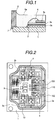
- Fig. 1 is a partial cross-sectional view of a module-type power semiconductor device of an embodiment according to the present invention.
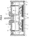
- Fig. 2 is a plan view of semiconductor circuits composed on an aluminum nitride substrate in the embodiment shown in Fig. 1.
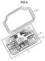
- Fig. 3 is a cross-sectional view showing the whole composition of the semiconductor device shown in Fig. 1.
- Fig. 4 is a plan view of semiconductor circuits composed on an aluminum nitride substrate in a power semiconductor device of another embodiment according to the present invention.
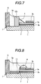
- Fig. 5 is a perspective plan view of semiconductor circuits composed on an aluminum nitride substrate in a power semiconductor device of another embodiment according to the present invention.
- Fig. 6 is a partial cross-sectional view of the semiconductor device of the embodiment shown in Fig. 5.
- Fig. 7 is a partial cross-sectional view of a module-type power semiconductor device of another embodiment according to the present invention.
- Fig. 8 is a partial cross-sectional view of a module-type power semiconductor device of another embodiment according to the present invention.
- Fig. 9 shows the relationship between the dielectric breakdown voltage and the creepage distance in the aluminum nitride substrate in the power semiconductor device of the embodiment.
- Fig. 10 is a cross-sectional view showing the composition of a conventional power semiconductor.
- Fig. 11 is a conceptual illustration showing the dielectric breakdown mechanism in the conventional semiconductor device.
- Fig. 12 is a conceptual illustration showing the dielectric breakdown mechanism in the conventional semiconductor device of the embodiment according to the present invention.
- Fig. 13 is a partial cross-sectional view of a power semiconductor device of an embodiment according to the present invention.
- Fig. 14 is a plan view of semiconductor circuits composed on an aluminum nitride substrate in the embodiment shown in Fig. 13.
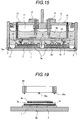
- Fig. 15 is a cross-sectional view showing the whole composition of the semiconductor device shown in Fig. 13.
- Fig. 16 is a partial cross-sectional view of a power semiconductor device of another embodiment according to the present invention.
- Fig. 17 is a partial cross-sectional view of a power semiconductor device of another embodiment according to the present invention.
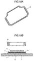
- Fig. 18A is a perspective view of the insulating resin frame in the semiconductor device of the embodiment shown in Fig. 17.
- Fig. 18B is a cross-sectional view of the insulating resin frame and the insulating substrate mounted on the base plate in the semiconductor device of the embodiment shown in Fig. 17.
- Fig. 19 is a cross-sectional view of a modified insulating resin frame and the insulating substrate mounted on the base plate, corresponding to Fig. 18B.
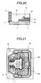
- Fig. 20 is a partial cross-sectional view of a power semiconductor device of another embodiment according to the present invention.
- Fig. 21 is a plan view of semiconductor circuits composed on an aluminum nitride substrate in the power semiconductor device of another embodiment shown in Fig. 20.
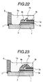
- Fig. 22 is a partial cross-sectional view of a power semiconductor device of another embodiment according to the present invention.
- Fig. 23 is a partial cross-sectional view of a power semiconductor device of another embodiment according to the present invention.
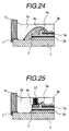
- Fig. 24 is a partial cross-sectional view of a power semiconductor device of another embodiment according to the present invention.
- Fig. 25 is a partial cross-sectional view of a power semiconductor device of another embodiment according to the present invention.
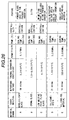
- Fig. 26 is a diagram tabling properties of various kinds of non-organic glass and resin.
- Fig. 1 is a partial cross-sectional view of a module-type power semiconductor device of an embodiment according to the present invention.
- an insulating ceramic substrate 3a such as an aluminum nitride (AlN) substrate, on whose top and back surface thin copper sheets 3b are attached, is mounted on a metal base plate 1 made of Al-SiC.
- the back surface of the aluminum nitride substrate 3a is facing the top surface of the base plate 1, and the thin copper sheet 3b attached on the back surface of the aluminum nitride substrate 3a is connected to the top surface of the base plate 1 with solder 2 such as (Sn-40%Pb) solder.
- solder 2 such as (Sn-40%Pb) solder.
- the peripheral edge part of the base plate 1 is adhered to the inside of an insulating resin case 6 with adhesive 7.
- the case 6 is filled with silicone insulating-gel resin 5a so that the gel resin 5a covers the aluminum nitride substrate 3a, the thin copper sheets 3b attached on the top and back surfaces of the substrate 3a, and silicone-resin 4, which will be explained later, covering the peripheral part of the substrate 3a.
- the surface of the aluminum nitride 3a, between the peripheral edge part of the aluminum nitride substrate 3a and the edge part of the thin copper sheet 3b attached on the substrate 3a, is covered with silicone-resin 4 as shown in Fig. 1.
- the withstand voltage (21 kVrms/mm) of the silicone-resin 4 is higher than that (14 kVrms/mm) of the insulating-gel resin 5a. Accordingly, the creepage withstand voltage of the aluminum nitride substrate 3a is improved in comparison with the semiconductor device in which the aluminum nitride substrate 3a is covered by only the insulating-gel resin 5a.
- the withstand voltage of the siclicone-resin 4 is higher than that (10 - 13 kVrms/mm) of the aluminum nitride substrate 3a. Furthermore, since the distance between the peripheral edge of the aluminum nitride substrate 3a and the edge of the thin copper sheet 3b attached on the substrate 3a is larger than the thickness of the aluminum nitride substrate 3a, the thickness of the silicone-resin 4 in the creepage direction is larger than the thickness of the aluminum nitride substrate 3a. Therefore, the dielectric breakdown voltage of the silicone-resin in the creepage direction is higher than the that of the aluminum nitride substrate 3a. Thus, since the dielectric breakdown hardly occurs on the creepage surface, and depends on only the aluminum nitride substrate 3a, the dielectric breakdown voltage can be easily determined and set.
- the edge and the part near the edge of the thin copper sheet 3b attached on the substrate 3a are also covered with the silicone-resin 4. Therefore, the part of high potential strength in the copper sheet 3b is covered with the silicone-resin 4, which also improves the creepage withstand voltage.
- the edge part of the silicone-resin 4 at the peripheral edge of the aluminum nitride substrate 3a is located within the peripheral surface of the substrate 3. That is, the silicone-resin 4 does not contact the surface of the base plate 1, between the connection part of the case 6 and the base plate 1, and the end side of the connection area of the base plate 1 and the substrate 3a. Therefore, even if the inner stress is generated between the silicone-resin 4 and the base plate 1 by the internal stress in the silicone-resin 4, due to expansion and contraction of the insulating-gel resin 5a or the silicone-resin 4, the stress is not generated between the base plate 1 and the silicone-resin 4.
- the withstand voltage does not easily decrease, which improves the reliability of the power semiconductor device.
- Fig. 2 is a plan view of semiconductor circuits composed on an aluminum nitride substrate in the embodiment shown in Fig. 1.
- a plurality of thin copper sheets 3b are attached on the aluminum nitride substrate 3a.
- semiconductor chips of power semiconductor elements such as IGBTs 100, diodes 110, etc., leader-line main terminals 9, leader-line auxiliary terminals 10, and so on are soldered on the copper sheets 3b.
- the copper sheet to which the leader-line main terminals 9 are soldered is electrically connected to each semiconductor chip with aluminum wires 200.
- the whole peripheral surface zone of the aluminum nitride substrate 3a is continuously covered with the silicone-resin 4. Accordingly, in the whole peripheral zone of the aluminum nitride substrate 3a, the creepage withstand voltage is increased, and the withstand voltage does not easily decrease. Thus, the reliability of the withstand voltage of the power semiconductor can be greatly improved.
- Fig. 3 is a cross-sectional view showing the whole composition of the semiconductor device shown in Fig. 1.
- a plurality of the aluminum nitride substrates 3a shown in Fig. 1 and Fig. 2 are soldered on the base plate 1, and the leader-line main and auxiliary terminals 9 and 10 are led out. Further, the leader-line main and auxiliary terminals 9 and 10 are passed through a terminal block 8, and a part of each of the leader-line main and auxiliary terminals 9 and 10, which is exposed outside the case 6, is connected to external circuits.
- the resin member of the case 6 is connected to the peripheral edge of the base plate 1.
- the terminal block 8 is also a cover of the case 6.
- the aluminum nitride substrates 3a, the leader-line main and auxiliary terminals 9 and 10, and the power semiconductor elements are contained in the case 6.
- the insulating-gel resin 5a is poured into the case 6, and the gel resin 5a covers the aluminum nitride substrates 3a, the copper sheets 3b attached on the substrates 3a, the connection parts of the copper sheets 3b and the leader-line main and auxiliary terminals 9 and 10, the power semiconductor elements, and the silicone-resin 4.
- the second-layer of insulating-gel resin 5b is poured on the first layer of the insulating-gel resin 5a.
- the void due to bubbles does not easily generate in the vicinity of the aluminum nitride substrates 3a, the copper sheets 3b attached on the substrates 3a, the connection parts of the copper sheets 3b, and the leader-line main and auxiliary terminals 9 and 10, the power semiconductor elements, and the surface of the silicone-resin 4 in the insulating-gel resin. Also, there is a space 11 between the terminal block 8 and the second-layer of the insulating-gel resin 5b in the case 6.
- the terminal block 8 is not pressed by the insulating-gel resin layers 5a and 5b. Accordingly, the stress in the silicone-resin 4, due to the expansion and contraction of the insulating-gel resin 5a and 5b, can be mitigated, which is effective to suppress the decrease in the withstand voltage of the power semiconductor device.
- the semiconductor circuits in the case 6 is composed as follows. First, the semiconductor chips are attached on the aluminum nitride substrates 3a with high melting point solder such as (Pb-5wt%Sn-1.5wt%Ag) solder by heating the chips and the solder at 350 °C in an H 2 ambience, and wiring is further performed for the chips by an aluminum bonding method. Afterward, the aluminum nitride substrates 3a are fixed on the base plate 1 with low melting point solder (for example, (Sn-40wt%Pb) solder by heating the substrates 3a and the solder at 240 °C in an H 2 ambience.
- high melting point solder such as (Pb-5wt%Sn-1.5wt%Ag) solder by heating the chips and the solder at 350 °C in an H 2 ambience
- wiring is further performed for the chips by an aluminum bonding method.
- the aluminum nitride substrates 3a are fixed on the base plate 1 with low melting point solder (for example, (Sn
- the silicone-resin 4 is applied to the whole peripheral zone of each aluminum nitride substrate 3a, between the edge part of the copper sheet 3b and the peripheral part of the substrate 3a, by using equipment such as a dispenser.
- this process should be performed so that the silicone-resin 4 does not flow out on the base plate 1.
- the applied silicone-resin 4 is heated at 150 °C for one hour in a thermostatic chamber to cure the resin 4.
- the leader-line main and auxiliary terminals 9 and 10 are soldered to the copper sheets 3b attached on the aluminum nitride substrates 3a, and the insulating resin case 6 is adhered to the peripheral of the base plate 1.
- the insulating-gel resin 5a and 5b are poured into the case 6, and the fabrication of the semiconductor device is completed by heating and curing the insulating-gel resin layers 5a and 5b after the degassing process has been performed for the poured gel resin.
- Fig. 9 shows the relationship between the dielectric breakdown voltage and the creepage distance in the aluminum nitride (AlN) substrate in the power semiconductor device of this embodiment, or in the conventional semiconductor device.
- AlN aluminum nitride
- Fig. 9 shows the relationship between the dielectric breakdown voltage and the creepage distance in the aluminum nitride (AlN) substrate in the power semiconductor device of this embodiment, or in the conventional semiconductor device.
- the dielectric breakdown voltage can be greatly improved.
- the improvement effect is larger than the effect obtained by geometrically lengthening the creepage distance.
- the dielectric breakdown occurs in the bulk of the insulating-gel resin 5a, or at the interface between the aluminum nitride substrate 3a and the insulating-gel resin 5a.
- the dielectric breakdown occurs in the silicone-resin 4 or the bulk of the aluminum nitride substrate 3a. This difference between the above two types of mechanisms in the dielectric breakdown causes the difference between the dialectic voltage values in the semiconductor device of this embodiment and the conventional semiconductor device.
- a protrusion of the silicone-resin 4 from the periphery of the aluminum nitride substrate 3a is permitted if the protrusion does not contact the surface of the base plate 1, between the connection part of the case 6 and the base plate 1, and the connection part of the aluminum nitride substrate 3a and base plate 1.
- the silicone-resin 4 can be replaced with material whose withstand voltage is higher than that of the substrate 3a, such as polyamide-resin whose withstand voltage is about 230 kVrms, polyimide-resin whose withstand voltage is about 200 kVrms, and the like.
- an insulating substrate made of alumina, or other kind of resin can be also used in place of the aluminum nitride substrate 3a.
- other metal or alloy other than copper can be used if it is conductive.
- brazing filler metal other than solder can be used to connect the aluminum nitride substrate 3a, the base plate 1, and to connect the copper sheet 3b, the semiconductor elements, and the leader-line terminals 9 and 10.
- Al-SiC is used for the base plate in Fig.
- the base plate 1 can be also made of Mo or W. Additionally, to improve the heat dissipation performance of the base plate 1, other metal such as copper or alloy can be used for the base plate 1. Meanwhile, in addition to IGBTs and diodes described in this embodiment, various types of semiconductor elements such as power transistors, MOSFETs, thyristors, and so on can be mounted on the substrates 23a in the case 6. Further, these semiconductor elements can be mounted on another substrate other than the aluminum nitride 3a and contained in the case 6. The above modifications are applicable to other embodiments according to the present invention.
- Fig. 4 is a plan view of semiconductor circuits composed on the aluminum nitride substrate 3a in a power semiconductor device of another embodiment according to the present invention.
- partial regions including at least corner parts in the peripheral zone of the aluminum nitride substrate 3a, at which the probability of the dielectric breakdown is comparatively high, are covered with the silicone-resin 4. This point is different from the embodiment shown in Fig. 2.
- This embodiment can also increase the dielectric breakdown voltage as shown in Fig. 9.
- the area to which the amount of the silicone-resin 4 is applied can be reduced, the time necessary to apply the silicone-resin 4 can be reduced, which improves the fabrication efficiency of the semiconductor devices, and the unevenness in the resin application can be also suppressed, which improves the yield of the semiconductor devices with a high dielectric breakdown voltage.
- Fig. 5 is a perspective plan view of semiconductor circuits composed on the aluminum nitride substrate 3a in a power semiconductor device of another embodiment according to the present invention.
- a frame 12a which is made of insulating resin such as PPS (poly phenylene sulfide), with an outline sectional shape equal to that of the peripheral zone in the aluminum nitride substrate 3a, is fabricated, and adhered to the peripheral zone in the aluminum nitride substrate 3a with the silicone-resin 4.
- PPS poly phenylene sulfide
- Fig. 6 is a partial cross-sectional view of the semiconductor device of the embodiment shown in Fig. 5.
- the PPS-resin frame 12a is adhered to the peripheral zone in the aluminum nitride substrate 3a, between the periphery edge of the substrate 3a and the edge part of the copper sheet 3a attached on the substrate 3a with the silicone-resin 4 also covering the peripheral zone. That is, the semiconductor device of this embodiment has the structure in which the PPS-resin frame 12a is attached on the silicone-resin 4 described in the embodiment shown in Fig. 1. According to this embodiment, the creepage distance in the aluminum nitride substrate 3a is practically increased by this PPS-resin frame 12a. Accordingly, the withstand voltage between the base plate 1 and the aluminum nitride substrate 3a is increased. Moreover, a frame made of other insulating material such as ceramics can be used in place of the PPS-resin frame 12a.
- Fig. 7 is a partial cross-sectional view of a power semiconductor device of another embodiment according to the present invention.
- the creepage distance in the aluminum nitride substrate 3a can be practically increased similar in the embodiment shown in Fig. 6.
- the inside shape of the frame 12b is equal to the periphery shape of the substrate 3a, and the frame 12b is adhered on the surface of the base plate 1, different from the frame 12a of the embodiment shown in Fig. 6.
- the aluminum nitride substrate 3a is surrounded by the frame 12b, and is soldered on the base plate 1.
- the surface of the aluminum nitride substrate 3a, between the peripheral part of the substrate 3a and the edge part of the copper sheet 3b attached on the substrate 3a, is covered with the silicone-resin 4.
- the inside wall of the PPS-resin frame 12b is adhered to the edge surface of the substrate 3a with the silicone-resin 4, and is supported by the substrate 3a.
- the creepage distance is secured by the PPS-resin frame 12b and the silicone-resin 4.
- a frame made of other insulating material such as ceramics can be used in place of the PPS-resin frame 12b.
- Fig. 8 is a partial cross-sectional view of a power semiconductor device of another embodiment according to the present invention.
- an insulating resin sheet 13 such as a polyimide-film is adhered on the surface of the aluminum nitride substrate 3a, between the peripheral part of the substrate 3 and the edge of the copper sheet 3b attached on the substrate 3.
- the creepage region between the peripheral part of the substrate 3 and the edge of the copper sheet 3b attached on the substrate 3, which also includes the surface of the resin sheet 13, is further covered with the silicone-resin 4.
- the creepage distance can be increased by only a little of the silicon-resin 4 along with the effects of the resin sheet 13 adhered on the creepage region of the aluminum nitride substrate 3a.
- the surface of the base plate 1, outside the aluminum nitride substrate 3a is also covered with the insulating resin sheet 13.
- This insulating resin sheet 13 covers the solder in the connection part of the base plate 1 and the aluminum nitride substrate 3a, and the copper sheet attached on the back surface of the substrate 3a. Further still, although not shown in Fig. 8, even if solder protrudes or projects from the connection part, the protruding or projecting solder is covered with the resin sheet 13. Therefore, the creepage distance is further increased, which also increases the withstand voltage of the substrate 3.
- an insulating module-type power semiconductor device with a withstand voltage of more than 4500V can be obtained.
- IGBT modules with the a withstand voltage of 5000V - 6000V can be obtained.
- an IGBT inverter for high-voltage power conversion can be composed with the IGBT modules of the present invention.
- the size of the IGBT inverter can be also decreased.
- Fig. 13 is a partial cross-sectional view of a power semiconductor device of an embodiment according to the present invention.
- the insulating substrate 3a made of insulating materiel such as aluminum nitride (AlN), on which the electrode pattern sheet 3b (for example, a copper film) is attached, is mounted on the base plate 1 made of metal such as Mo, composite material such as Al-SiC, or sintered material such CuCuO 2 , with solder 2, for example, (Sn-40wt%Pb) solder.
- AlN aluminum nitride
- solder 2 for example, (Sn-40wt%Pb) solder.
- the region of the insulating substrate 3a, between the edge part of the substrate 3a and the edge part of the electrode pattern sheet 3b, - that is, the creepage surface in the peripheral part of the substrate 3a -, is covered with resin 4 possessing a high withstand voltage higher than that of insulating-gel material such as silicone-gel resin whose dielectric breakdown voltage is 14 kVrms.
- resin 4 possessing a high withstand voltage higher than that of insulating-gel material such as silicone-gel resin whose dielectric breakdown voltage is 14 kVrms.
- silicon-resin whose dielectric breakdown voltage is 21 kvrms, polyamide-resin whose dielectric breakdown voltage is 230 kVrms, etc. can be used for the resin 4.
- a case member 6 made of insulating resin is adhered to peripheral part of the base plate 1 with adhesive 7.
- the surface of the base plate 1, between the case member 6 and the peripheral part of the substrate 3a, is covered with another resin 37 possessing a high withstand voltage, and the insulating-gel material 5a is poured on the substrate 3, the silicon-resin 4, and the resin 37 in the case member 6.
- the resin 37 with a high withstand voltage is poured into the case member 6 until the resin 37 contacts the inside wall of the case member 6, the insulating substrate 3a, and the resin 4 with a high withstand voltage.
- the surface of the base plate 1 is filled with the resin 37 without any opening.
- the same kind or different kinds of resin can be used for the resin 4 and 37 with a high withstand voltage if the resin to be used possesses the dielectric breakdown voltage higher than that of the insulating-gel material 5b.
- Fig. 14 is a plan view of semiconductor circuits composed on an aluminum nitride substrate in the embodiment shown in Fig. 13, and Fig. 15 is a cross-sectional view showing the whole composition of the semiconductor device shown in Fig. 14.
- Fig. 14 which is an enlarged plan view of the composition of semiconductor circuits mounted on one insulating substrate
- the semiconductor chips 16a and 16b are attached on the insulating substrate 3a with high melting point solder such as (Pb-5wt%Sn-1.5w%Ag) solder with the melting point of 296 - 305 °C by heating the chips and the solder at 350 °C in an H 2 ambience.
- high melting point solder such as (Pb-5wt%Sn-1.5w%Ag) solder with the melting point of 296 - 305 °C by heating the chips and the solder at 350 °C in an H 2 ambience.
- aluminum wire bonding is performed for the semiconductor chips 16a and 16b with aluminum wires.
- the insulating substrate 3a is connected on the base plate 1 with low melting point solder such as (Pb-60wt%Sn) solder by heating the substrate 3a and the solder at 240 °C in an H 2 ambience.
- the surface of the substrate 3a, between the peripheral part of substrate 3a and the edge part of the electrode pattern sheet 3b, is covered with the resin 4 possessing a high withstand voltage.
- the resin 4 with a high withstand voltage on the substrate 3a is cured by heating the resin 4 in a thermostatic oven (150 °C ⁇ lh).
- the leader-line terminals 9 and 10 are connected on the substrate 3a with solder paste such as (Pb-60wt%Sn) paste by heating the terminals 9 and 10 and the solder paste at 240 °C.
- the insulating resin case member 6 is adhered to the peripheral part of the base plate 1 with the adhesive 7 shown in Fig. 13. Furthermore, the surface of the base plate 1, between the case member 6 and the edge part of the insulating substrate 3a covered with resin 4, is further covered with the resin 37 possessing a high withstand voltage. Afterward, the insulating silicone-gel material 5b is poured into the case member 6 so that a space 11 remains under the terminal block 8 provided as a cover of the case member 6. Moreover, after the degassing process is performed for the poured silicone-gel material 37 (1 Trr ⁇ 80 m), the silicon gel material 37 is heated and cured (150 °C ⁇ 2 h). Thus, the fabrication of the semiconductor device is completed.
- the withstand voltage can be further improved.
- the resin 37 whose dielectric breakdown voltage is higher than that of the insulating-gel material 5a and 5b is used, the withstand voltage is greatly improved.
- the resin 37 covering the surface of the base plate 1 does not flow or extend onto the insulating substrate 3a or the electrode pattern sheet 3b.
- the electrode pattern sheet 3b is surrounded by the annular cover zone of the resins 4, and does not contact the resin 37. Therefore, each stress generated at interfaces among the resin 37, the base plate 1, and the insulating plate 3a is mitigated, which decreases the probability of occurrence of a separation in the semiconductor device. Thus, the dielectric breakdown voltage is not easily degraded, and the reliability of the semiconductor device is improved.
- Fig. 16 is a partial cross-sectional view of a power semiconductor device of another embodiment according to the present invention.
- the creepage surface of the insulating substrate 3a, and a partial zone of the surface of the base plate 1, surrounding the substrate 3a are covered with the resin 4 with possessing a high withstand voltage, and the resin 4 is cured.
- the remaining surface of the base plate 1, between the case member 6 and the resin 4 is further covered with the resin 37 possessing high withstand voltage.
- it is desirable that the shape and size of the electrode pattern sheet 3b attached at the edge of the base plate 1 is almost the same as that of the insulating substrate 3a.
- the intrusion of the resin 4 into the gap between the substrate 3a and the base plate 1 - that is, the space under the back surface of the substrate 3a- can be prevented. Therefore, the break at the edge part of the insulating substrate 3a due to the intrusion of the resin 4 can be prevented.
- the semiconductor device of this embodiment possesses almost the same dielectric breakdown voltage as that of the device of the embodiment shown in Fig. 13.
- Fig. 17 is a partial cross-sectional view of a power semiconductor device of another embodiment according to the present invention, and the whole composition of the semiconductor device of this embodiment is almost the same as that of the device shown in Fig. 15.
- an insulating resin frame 39 is connected on the peripheral creepage zone of the insulating substrate 3a with the rein 4 possessing a high withstand voltage, and the surface of the base plate 1, between the frame 39 and the case member 6, is covered with the resin 37 possessing a high withstand voltage, similar to the embodiment shown in Fig. 16.
- the insulating resin for example, PPS-resin
- ceramics frame 39 whose cross-sectional shape is almost equal to that of the peripheral creepage zone of the substrate 3a, it is possible to secure the creepage distance longer than twice of that in the conventional structure.
- the surface of the base plate 1, between the case member 6 and the frame 39 is thickly covered with the resin 37 possessing a high withstand voltage.
- the dielectric breakdown voltage between the insulating substrate 3a and the base plate 1 is greatly increased.
- Fig. 18A is a perspective view of the insulating resin (for example, PPS-resin) or ceramic frame 39 in the semiconductor device of the embodiment shown in Fig. 17, and Fig. 18B shows cross-sectional views of the insulating resin frame 39 and the insulating substrate 3a mounted on the base plate 1. Further, Fig. 19 shows cross-sectional views of a modified insulating resin frame 39 and the insulating substrate 3a mounted on the base plate 1, which corresponds to Fig. 18B.
- the insulating resin for example, PPS-resin
- Fig. 19 shows cross-sectional views of a modified insulating resin frame 39 and the insulating substrate 3a mounted on the base plate 1, which corresponds to Fig. 18B.
- projection parts 39a are provided on the back surface of the insulating resin frame 39, the back surface corresponding to the peripheral zone of the insulating substrate 3a. Accordingly, the frame 39 can be easily positioned on the peripheral zone of the substrate 3a, which certainly secures the creepage distance of the insulating substrate 3a. Moreover, by providing three or more projection parts on the back surface of the frame 39, the distance between the back surface of the frame 39 and the peripheral surface of the insulating substrate 3a - that is, the thickness of the resin 4 with a high withstand voltage - can be kept constant, which results in the high adhesive strength in the connection between the frame 39 and the substrate 3a. Thus, a more reliable insulating-withstand-voltage-structure can be realized for the semiconductor device.
- the withstand voltage of material used for the insulating substrate 3a in the conventional semiconductor device and that in the device according to the present invention is expressed by the dielectric breakdown voltage of 10 - 13 kVrms.
- the dielectric breakdown voltage of the gel resin 5a (5b) which is used in the above two types of devices is about 14 kVrms. Therefore, the maximum withstand voltage is about 14 kVrms in the conventional semiconductor device.
- the creepage region of the insulating substrate 3a, between the peripheral part of the substrate 3a and the edge part of the electrode pattern sheet 3b, is covered with the resin 4 possessing a high withstand voltage (high dielectric breakdown voltage).
- the surface of the base plate 1, between the case member 6 and the periphery of the insulating substrate 3a is covered with the resin 4 possessing a high withstand voltage, or the insulating resin frame 39 is attached on the peripheral creepage zone of the insulating substrate 3a.
- the dielectric breakdown occurs in the bulk of the gel resin or at the interface between the insulating substrate 3a and the gel resin in the conventional structure, the dielectric breakdown passes through the resin 4 with a high withstand voltage or the breakdown occurs in the substrate 3a in the structure according to the present invention. Therefore, in accordance with the present invention, greatly larger effects to increase the withstand voltage can be obtained in comparison with the measure of geometrically increasing the creepage distance of the insulating substrate 3a in the conventional structure. Thus, the semiconductor device with a high withstand voltage can be obtained without increasing the size of the insulating substrate.
- Fig. 20 is a partial cross-sectional view of a power semiconductor device of another embodiment according to the present invention
- Fig. 21 is a plan view of semiconductor circuits composed on an aluminum nitride substrate in the power semiconductor device of the embodiment.
- electrode pattern sheets 3b are soldered on the top and back surfaces of the insulating substrate 3a made of insulating material such as aluminum nitride (AlN), with Ag solder such as Cu-Ag eutectic solder containing Ti, with the melting point of 800 - 850 °C.
- the boundary part between the creepage surface of the substrate 3a and the edge part of the electrode pattern sheet 3b is covered with non-organic crystal glass 4a such as (Bi 2 O 3 -B 2 O 3 ) glass, and the glass 4a is fused and fixed to the substrate 3a and the electrode pattern sheet 3b by heating the glass at 700 °C in atmosphere or N 2 gas.
- the semiconductor chips 400 are attached on the electrode pattern sheet 3b with high melting point solder such as (Pb-5wt%Sn-1.5wt%Ag) solder with the melting point of 296 - 305 °C, and wiring is performed for the semiconductor chips 400 with aluminum wires 300.
- the AlN insulating substrates 3a are attached on the base plate 1 made of metal such as Mo, composite material such as Al-SiC, or sintered material such as CuCuO 2 , with solder 2, for example, (Sn-40 wt% Pb) solder with the melting point of 183 - 191 °C, by heating the substrates 3a and the solder in H 2 gas.
- the case member 6 made of PPS insulating resin is attached around the peripheral part of the base plate 1 with silicone-resin adhesive 7.
- the insulating-gel resin 5a is poured into the case member 6, and is cured, the fabrication of the module-type semiconductor device is completed by sealing the upper aperture of the case member 6.
- the withstand voltage between the edge part of the electrode pattern sheet 3b and the base plate 1 can be greatly increased.
- the frame positioned and connected around the peripheral creepage region of the insulating substrate 3a is made of the same resin making the case member 6 or ceramics similar to that making the insulating substrate 3a, the high withstand voltage of the semiconductor device can be secured.
- material used for the base plate 1 is selected such that the thermal expansion coefficient of the base plate 1 on which the insulating substrate 3a is soldered, the electrode pattern sheet 3b being attached on the insulating substrate 3a, is less than three times of that of silicon (Si). Accordingly, in the operation state of the semiconductor device, the difference between thermal expansion coefficients of the substrate 3a and the base plate 1 can be reduced, and the thermal stress applied to the solder 2 can be also mitigated, which realizes a highly reliable semiconductor device.
- metal such as Mo, composite material such as Al-SiC, sintered material such as CuCuO 2 , and so on are desirable as material used for the base plate 1.
- Figs. 22, 23, and 24 are partial cross-sectional views of power semiconductor device of other embodiments according to the present invention.
- the boundary part between the creepage surface of the substrate 3a and the edge part of the electrode pattern sheet 3b is covered with non-organic crystal glass 4a such as (Bi 2 O 3 -B 2 O 3 ) glass, and the remaining creepage surface of the substrate 3a is covered with silicone-resin 4b of high insulating-withstand-voltage resin shown by symbol D in Fig. 26.
- non-organic crystal glass 4a such as (Bi 2 O 3 -B 2 O 3 ) glass
- silicone-resin 4b of high insulating-withstand-voltage resin shown by symbol D in Fig. 26.
- silicone-resin 4b of high insulating-withstand-voltage resin shown by symbol D in Fig. 26.
- the breakdown development due to local-discharge in the creepage surface of the AlN insulating substrate 3a can be suppressed by the two-step barriers 4a and 4b, which further increases the withstand voltage.
- the non-organic cover 4a on the boundary part between the substrate 3a and the conductive sheet 3b is protected by the insulating resin 4b, and the withstand voltage is further increased by the double barriers 4a and 4b.
- the withstand voltage in the partial surface of the base plate 1, surrounding the periphery of the substrate 3a can be also additionally obtained.
- the potential concentration at the edge part of the electrode pattern sheet 3b is mitigated by the first layer of the non-organic cover 4a, and the region neighboring or surrounding the non-organic cover 4a is protected by the second layer of the insulating resin 4b.
- the breakdown development due to the local-discharge in the creepage surface of the AlN insulating substrate 3a can be sufficiently suppressed, which brings the very high withstand voltage to the semiconductor device.
- silicone-resin or polyamide-resin which well adheres to the creepage surface of the AlN insulating substrate 3a and is easily obtained, is used for the resin 4a with a high withstand voltage. Therefore, the semiconductor device can be easily and cheaply fabricated.
- Fig. 25 is a partial cross-sectional view of a power semiconductor device of another embodiment according to the present invention.
- the insulating frame 12 made of PPS-resin or ceramics is adhered on the remaining creepage zone in the peripheral part of the insulating substrate 3a with the silicone-resin 4b possessing a high withstand voltage.
- the creepage distance of the insulating substrate 3b can be elongated by more than twice, which can realize the semiconductor device with the withstand voltage greatly higher than that of the conventional semiconductor device.
- the reliability in the withstand voltage of a semiconductor device can be greatly improved.
Landscapes
- Structures Or Materials For Encapsulating Or Coating Semiconductor Devices Or Solid State Devices (AREA)
Applications Claiming Priority (4)
| Application Number | Priority Date | Filing Date | Title |
|---|---|---|---|
| JP14689698 | 1998-05-28 | ||
| JP14689698A JP3440824B2 (ja) | 1998-05-28 | 1998-05-28 | 半導体装置 |
| JP1146599 | 1999-01-20 | ||
| JP11011465A JP2000216332A (ja) | 1999-01-20 | 1999-01-20 | 半導体装置 |
Publications (3)
| Publication Number | Publication Date |
|---|---|
| EP0962974A2 true EP0962974A2 (fr) | 1999-12-08 |
| EP0962974A3 EP0962974A3 (fr) | 2002-04-03 |
| EP0962974B1 EP0962974B1 (fr) | 2005-01-26 |
Family
ID=26346892
Family Applications (1)
| Application Number | Title | Priority Date | Filing Date |
|---|---|---|---|
| EP99303988A Expired - Lifetime EP0962974B1 (fr) | 1998-05-28 | 1999-05-24 | Dispositif semi-conducteur |
Country Status (3)
| Country | Link |
|---|---|
| EP (1) | EP0962974B1 (fr) |
| DE (1) | DE69923374T2 (fr) |
| RU (1) | RU2165115C2 (fr) |
Cited By (18)
| Publication number | Priority date | Publication date | Assignee | Title |
|---|---|---|---|---|
| EP1193761A2 (fr) | 2000-09-29 | 2002-04-03 | Kabushiki Kaisha Toshiba | Dispositif semi-conducteur comprenant un dispositif de connection intermédiaire |
| WO2003001594A3 (fr) * | 2001-06-25 | 2003-11-06 | Eupec Gmbh & Co Kg | Module haute tension et son procede de production |
| EP1465250A1 (fr) * | 2003-04-02 | 2004-10-06 | Abb Research Ltd. | Module de puissance à semi-conducteur isolé à décharge partielle reduite et sa méthode de production |
| WO2005096374A1 (fr) * | 2004-03-15 | 2005-10-13 | Siemens Aktiengesellschaft | Produit electrotechnique comprenant un element electrique et une masse de scellement pour l'isolation electrique de l'element, et procede de fabrication associe |
| DE10312238B4 (de) * | 2002-07-15 | 2008-09-04 | Mitsubishi Denki K.K. | Leistungshalbleitereinrichtung |
| DE102007041229A1 (de) * | 2007-08-31 | 2009-03-05 | Fraunhofer-Gesellschaft zur Förderung der angewandten Forschung e.V. | Schaltungsanordnung und ein Verfahren zum Verkapseln derselben |
| EP2302676A1 (fr) * | 2009-09-29 | 2011-03-30 | ABB Technology AG | Dispositif semi-conducteur haute puissance |
| CN103222053A (zh) * | 2010-09-24 | 2013-07-24 | 半导体元件工业有限责任公司 | 电路装置 |
| WO2015074431A1 (fr) * | 2013-11-21 | 2015-05-28 | 西安永电电气有限责任公司 | Module igbt haute tension à atténuation de décharge partielle et son procédé de fabrication |
| US9048227B2 (en) | 2013-02-13 | 2015-06-02 | Mitsubishi Electric Corporation | Semiconductor device |
| DE102014110455A1 (de) * | 2014-07-24 | 2016-01-28 | Infineon Technologies Ag | Verfahren zur Herstellung eines Elektronenmoduls mit Vergussmasse |
| CN105304619A (zh) * | 2014-05-28 | 2016-02-03 | 株洲南车时代电气股份有限公司 | 一种igbt衬板结构及其制作方法 |
| WO2016044179A3 (fr) * | 2014-09-15 | 2016-05-12 | Invensas Corporation | Structures électroniques renforcées de couches poreuses et non poreuses, et procédés de fabrication |
| US9466548B2 (en) | 2012-02-22 | 2016-10-11 | Mitsubishi Electric Corporation | Semiconductor device and method of manufacturing semiconductor device |
| WO2019011890A1 (fr) * | 2017-07-12 | 2019-01-17 | Abb Schweiz Ag | Module semi-conducteur de puissance |
| EP3518278A1 (fr) * | 2018-01-30 | 2019-07-31 | Infineon Technologies AG | Module semi-conducteur de puissance et procédé de sa fabrication |
| FR3084964A1 (fr) * | 2018-08-09 | 2020-02-14 | Universite Toulouse Iii - Paul Sabatier | Dispositif electronique presentant une isolation electrique multicouche, et procede de fabrication correspondant. |
| US11916001B2 (en) | 2018-03-14 | 2024-02-27 | Mitsubishi Electric Corporation | Semiconductor power module and power conversion device |
Families Citing this family (2)
| Publication number | Priority date | Publication date | Assignee | Title |
|---|---|---|---|---|
| CN109743882B (zh) | 2016-09-21 | 2022-12-30 | 三菱电机株式会社 | 半导体装置以及电力变换装置 |
| JP2023134143A (ja) * | 2022-03-14 | 2023-09-27 | 富士電機株式会社 | 半導体モジュール、半導体装置、及び車両 |
Family Cites Families (7)
| Publication number | Priority date | Publication date | Assignee | Title |
|---|---|---|---|---|
| DE3309679A1 (de) * | 1983-03-17 | 1984-09-20 | Siemens AG, 1000 Berlin und 8000 München | Halbleiterbauelement mit giessharzfuellung |
| JPS6164144A (ja) * | 1984-09-05 | 1986-04-02 | Mitsubishi Electric Corp | 半導体装置 |
| JPH063819B2 (ja) * | 1989-04-17 | 1994-01-12 | セイコーエプソン株式会社 | 半導体装置の実装構造および実装方法 |
| JPH06268094A (ja) * | 1993-03-12 | 1994-09-22 | Sanyo Electric Co Ltd | 混成集積回路 |
| JPH06334070A (ja) * | 1993-05-27 | 1994-12-02 | Sanyo Electric Co Ltd | 混成集積回路装置 |
| JPH08125071A (ja) * | 1994-10-25 | 1996-05-17 | Fuji Electric Co Ltd | 半導体装置 |
| CA2255441C (fr) * | 1997-12-08 | 2003-08-05 | Hiroki Sekiya | Boitier pour dispositif d'alimentation a semiconducteurs et methode d'assemblage connexe |
-
1999
- 1999-05-24 DE DE69923374T patent/DE69923374T2/de not_active Expired - Lifetime
- 1999-05-24 EP EP99303988A patent/EP0962974B1/fr not_active Expired - Lifetime
- 1999-05-27 RU RU99111593/28A patent/RU2165115C2/ru not_active IP Right Cessation
Cited By (30)
| Publication number | Priority date | Publication date | Assignee | Title |
|---|---|---|---|---|
| EP1193761A2 (fr) | 2000-09-29 | 2002-04-03 | Kabushiki Kaisha Toshiba | Dispositif semi-conducteur comprenant un dispositif de connection intermédiaire |
| EP1193761A3 (fr) * | 2000-09-29 | 2005-03-09 | Kabushiki Kaisha Toshiba | Dispositif semi-conducteur comprenant un dispositif de connection intermédiaire |
| US7078795B2 (en) | 2001-06-25 | 2006-07-18 | Eupec Europaische Gesellschaft Fur Leistungshalbleiter Gmbh & Co. Kg | High voltage module and method for producing same |
| WO2003001594A3 (fr) * | 2001-06-25 | 2003-11-06 | Eupec Gmbh & Co Kg | Module haute tension et son procede de production |
| US7407836B2 (en) | 2001-06-25 | 2008-08-05 | Infineon Technologies Ag | High-voltage module and method for producing same |
| DE10312238B4 (de) * | 2002-07-15 | 2008-09-04 | Mitsubishi Denki K.K. | Leistungshalbleitereinrichtung |
| WO2004088748A1 (fr) * | 2003-04-02 | 2004-10-14 | Abb Research Ltd | Module semi-conducteur isole presentant une decharge partielle limitee et son procede de fabrication |
| CN100444358C (zh) * | 2003-04-02 | 2008-12-17 | Abb研究有限公司 | 局部放电减少的绝缘功率半导体模块及制造方法 |
| EP1465250A1 (fr) * | 2003-04-02 | 2004-10-06 | Abb Research Ltd. | Module de puissance à semi-conducteur isolé à décharge partielle reduite et sa méthode de production |
| WO2005096374A1 (fr) * | 2004-03-15 | 2005-10-13 | Siemens Aktiengesellschaft | Produit electrotechnique comprenant un element electrique et une masse de scellement pour l'isolation electrique de l'element, et procede de fabrication associe |
| DE102007041229A1 (de) * | 2007-08-31 | 2009-03-05 | Fraunhofer-Gesellschaft zur Förderung der angewandten Forschung e.V. | Schaltungsanordnung und ein Verfahren zum Verkapseln derselben |
| EP2302676A1 (fr) * | 2009-09-29 | 2011-03-30 | ABB Technology AG | Dispositif semi-conducteur haute puissance |
| US9271397B2 (en) | 2010-09-24 | 2016-02-23 | Semiconductor Components Industries, Llc | Circuit device |
| CN103222053A (zh) * | 2010-09-24 | 2013-07-24 | 半导体元件工业有限责任公司 | 电路装置 |
| US9466548B2 (en) | 2012-02-22 | 2016-10-11 | Mitsubishi Electric Corporation | Semiconductor device and method of manufacturing semiconductor device |
| US9048227B2 (en) | 2013-02-13 | 2015-06-02 | Mitsubishi Electric Corporation | Semiconductor device |
| WO2015074431A1 (fr) * | 2013-11-21 | 2015-05-28 | 西安永电电气有限责任公司 | Module igbt haute tension à atténuation de décharge partielle et son procédé de fabrication |
| CN105304619A (zh) * | 2014-05-28 | 2016-02-03 | 株洲南车时代电气股份有限公司 | 一种igbt衬板结构及其制作方法 |
| DE102014110455A1 (de) * | 2014-07-24 | 2016-01-28 | Infineon Technologies Ag | Verfahren zur Herstellung eines Elektronenmoduls mit Vergussmasse |
| DE102014110455B4 (de) * | 2014-07-24 | 2016-06-09 | Infineon Technologies Ag | Verfahren zur Herstellung eines Elektronikmoduls mit Vergussmasse |
| WO2016044179A3 (fr) * | 2014-09-15 | 2016-05-12 | Invensas Corporation | Structures électroniques renforcées de couches poreuses et non poreuses, et procédés de fabrication |
| US9799626B2 (en) | 2014-09-15 | 2017-10-24 | Invensas Corporation | Semiconductor packages and other circuit modules with porous and non-porous stabilizing layers |
| WO2019011890A1 (fr) * | 2017-07-12 | 2019-01-17 | Abb Schweiz Ag | Module semi-conducteur de puissance |
| JP2020526930A (ja) * | 2017-07-12 | 2020-08-31 | アー・ベー・ベー・パワー・グリッズ・スウィツァーランド・アクチェンゲゼルシャフトAbb Power Grids Switzerland Ag | パワー半導体モジュール |
| US11362008B2 (en) | 2017-07-12 | 2022-06-14 | Hitachi Energy Switzerland Ag | Power semiconductor module embedded in a mold compounded with an opening |
| EP3518278A1 (fr) * | 2018-01-30 | 2019-07-31 | Infineon Technologies AG | Module semi-conducteur de puissance et procédé de sa fabrication |
| US11081414B2 (en) | 2018-01-30 | 2021-08-03 | Infineon Technologies Ag | Power semiconductor module arrangement |
| US11557522B2 (en) | 2018-01-30 | 2023-01-17 | Infineon Technologies Ag | Method for producing power semiconductor module arrangement |
| US11916001B2 (en) | 2018-03-14 | 2024-02-27 | Mitsubishi Electric Corporation | Semiconductor power module and power conversion device |
| FR3084964A1 (fr) * | 2018-08-09 | 2020-02-14 | Universite Toulouse Iii - Paul Sabatier | Dispositif electronique presentant une isolation electrique multicouche, et procede de fabrication correspondant. |
Also Published As
| Publication number | Publication date |
|---|---|
| EP0962974A3 (fr) | 2002-04-03 |
| EP0962974B1 (fr) | 2005-01-26 |
| RU2165115C2 (ru) | 2001-04-10 |
| DE69923374T2 (de) | 2006-01-19 |
| DE69923374D1 (de) | 2005-03-03 |
Similar Documents
| Publication | Publication Date | Title |
|---|---|---|
| EP0962974B1 (fr) | Dispositif semi-conducteur | |
| US20250357433A1 (en) | Semiconductor device | |
| US8546926B2 (en) | Power converter | |
| US11201121B2 (en) | Semiconductor device | |
| US11942449B2 (en) | Semiconductor arrangement and method for producing the same | |
| JP2002076197A (ja) | 半導体装置用基板及び半導体装置 | |
| US9466542B2 (en) | Semiconductor device | |
| CN112786550B (zh) | 半导体装置 | |
| EP1739740A2 (fr) | Semiconducteur à puissance | |
| JP3440824B2 (ja) | 半導体装置 | |
| US12564094B2 (en) | Power semiconductor module arrangement and method for producing the same | |
| CN110447099B (zh) | 半导体器件 | |
| CN112530915B (zh) | 半导体装置 | |
| JPH10173098A (ja) | パワー半導体装置およびその製法 | |
| CA2339523A1 (fr) | Composant plat a semi-conducteur, son procede de fabrication et convertisseur comprenant ce composant | |
| CN111834307B (zh) | 半导体模块 | |
| JP2000091472A (ja) | 半導体装置 | |
| JP7157783B2 (ja) | 半導体モジュールの製造方法及び半導体モジュール | |
| JP2025025374A (ja) | 半導体装置および半導体装置の製造方法 | |
| CN111033723A (zh) | 功率半导体模块 | |
| JP2023170416A (ja) | 半導体モジュール及び電力変換装置 | |
| CN116960066A (zh) | 功率半导体模块装置和用于制造功率半导体模块装置的方法 | |
| CN121890326A (zh) | 半导体装置 | |
| CN118841375A (zh) | 半导体装置、半导体模块及半导体模块的制造方法 | |
| CN120322865A (zh) | 半导体装置、电力转换装置及其制造方法 |
Legal Events
| Date | Code | Title | Description |
|---|---|---|---|
| PUAI | Public reference made under article 153(3) epc to a published international application that has entered the european phase |
Free format text: ORIGINAL CODE: 0009012 |
|
| 17P | Request for examination filed |
Effective date: 19990614 |
|
| AK | Designated contracting states |
Kind code of ref document: A2 Designated state(s): AT BE CH CY DE DK ES FI FR GB GR IE IT LI LU MC NL PT SE Kind code of ref document: A2 Designated state(s): DE FR GB |
|
| AX | Request for extension of the european patent |
Free format text: AL;LT;LV;MK;RO;SI |
|
| PUAL | Search report despatched |
Free format text: ORIGINAL CODE: 0009013 |
|
| AK | Designated contracting states |
Kind code of ref document: A3 Designated state(s): AT BE CH CY DE DK ES FI FR GB GR IE IT LI LU MC NL PT SE |
|
| AX | Request for extension of the european patent |
Free format text: AL;LT;LV;MK;RO;SI |
|
| RIC1 | Information provided on ipc code assigned before grant |
Free format text: 7H 01L 23/24 A, 7H 01L 25/07 B |
|
| AKX | Designation fees paid |
Free format text: DE FR GB |
|
| 17Q | First examination report despatched |
Effective date: 20031006 |
|
| GRAP | Despatch of communication of intention to grant a patent |
Free format text: ORIGINAL CODE: EPIDOSNIGR1 |
|
| GRAS | Grant fee paid |
Free format text: ORIGINAL CODE: EPIDOSNIGR3 |
|
| GRAA | (expected) grant |
Free format text: ORIGINAL CODE: 0009210 |
|
| AK | Designated contracting states |
Kind code of ref document: B1 Designated state(s): DE FR GB |
|
| REG | Reference to a national code |
Ref country code: GB Ref legal event code: FG4D |
|
| REG | Reference to a national code |
Ref country code: IE Ref legal event code: FG4D |
|
| REF | Corresponds to: |
Ref document number: 69923374 Country of ref document: DE Date of ref document: 20050303 Kind code of ref document: P |
|
| PLBE | No opposition filed within time limit |
Free format text: ORIGINAL CODE: 0009261 |
|
| STAA | Information on the status of an ep patent application or granted ep patent |
Free format text: STATUS: NO OPPOSITION FILED WITHIN TIME LIMIT |
|
| ET | Fr: translation filed | ||
| 26N | No opposition filed |
Effective date: 20051027 |
|
| REG | Reference to a national code |
Ref country code: DE Ref legal event code: R082 Ref document number: 69923374 Country of ref document: DE Representative=s name: PATENTANWAELTE STREHL, SCHUEBEL-HOPF & PARTNER, DE |
|
| REG | Reference to a national code |
Ref country code: DE Ref legal event code: R082 Ref document number: 69923374 Country of ref document: DE Representative=s name: STREHL SCHUEBEL-HOPF & PARTNER MBB PATENTANWAE, DE Effective date: 20141127 Ref country code: DE Ref legal event code: R082 Ref document number: 69923374 Country of ref document: DE Representative=s name: PATENTANWAELTE STREHL, SCHUEBEL-HOPF & PARTNER, DE Effective date: 20141127 Ref country code: DE Ref legal event code: R081 Ref document number: 69923374 Country of ref document: DE Owner name: HITACHI POWER SEMICONDUCTOR DEVICE, LTD., HITA, JP Free format text: FORMER OWNER: HITACHI, LTD., TOKYO, JP Effective date: 20141127 Ref country code: GB Ref legal event code: 732E Free format text: REGISTERED BETWEEN 20141204 AND 20141211 |
|
| REG | Reference to a national code |
Ref country code: FR Ref legal event code: TP Owner name: HITACHI POWER SEMICONDUCTOR DEVICE, LTD., JP Effective date: 20141209 Ref country code: FR Ref legal event code: CA Effective date: 20141209 |
|
| REG | Reference to a national code |
Ref country code: FR Ref legal event code: PLFP Year of fee payment: 18 |
|
| REG | Reference to a national code |
Ref country code: FR Ref legal event code: PLFP Year of fee payment: 19 |
|
| REG | Reference to a national code |
Ref country code: FR Ref legal event code: PLFP Year of fee payment: 20 |
|
| PGFP | Annual fee paid to national office [announced via postgrant information from national office to epo] |
Ref country code: GB Payment date: 20180329 Year of fee payment: 20 |
|
| PGFP | Annual fee paid to national office [announced via postgrant information from national office to epo] |
Ref country code: DE Payment date: 20180508 Year of fee payment: 20 |
|
| PGFP | Annual fee paid to national office [announced via postgrant information from national office to epo] |
Ref country code: FR Payment date: 20180412 Year of fee payment: 20 |
|
| REG | Reference to a national code |
Ref country code: DE Ref legal event code: R071 Ref document number: 69923374 Country of ref document: DE |
|
| REG | Reference to a national code |
Ref country code: GB Ref legal event code: PE20 Expiry date: 20190523 |
|
| PG25 | Lapsed in a contracting state [announced via postgrant information from national office to epo] |
Ref country code: GB Free format text: LAPSE BECAUSE OF EXPIRATION OF PROTECTION Effective date: 20190523 |