EP2302676A1 - Dispositif semi-conducteur haute puissance - Google Patents
Dispositif semi-conducteur haute puissance Download PDFInfo
- Publication number
- EP2302676A1 EP2302676A1 EP09171605A EP09171605A EP2302676A1 EP 2302676 A1 EP2302676 A1 EP 2302676A1 EP 09171605 A EP09171605 A EP 09171605A EP 09171605 A EP09171605 A EP 09171605A EP 2302676 A1 EP2302676 A1 EP 2302676A1
- Authority
- EP
- European Patent Office
- Prior art keywords
- conductive layer
- barrier
- substrate
- high power
- power semiconductor
- Prior art date
- Legal status (The legal status is an assumption and is not a legal conclusion. Google has not performed a legal analysis and makes no representation as to the accuracy of the status listed.)
- Withdrawn
Links
Images
Classifications
-
- H—ELECTRICITY
- H10—SEMICONDUCTOR DEVICES; ELECTRIC SOLID-STATE DEVICES NOT OTHERWISE PROVIDED FOR
- H10W—GENERIC PACKAGES, INTERCONNECTIONS, CONNECTORS OR OTHER CONSTRUCTIONAL DETAILS OF DEVICES COVERED BY CLASS H10
- H10W42/00—Arrangements for protection of devices
- H10W42/60—Arrangements for protection of devices protecting against electrostatic charges or discharges, e.g. Faraday shields
-
- H—ELECTRICITY
- H10—SEMICONDUCTOR DEVICES; ELECTRIC SOLID-STATE DEVICES NOT OTHERWISE PROVIDED FOR
- H10W—GENERIC PACKAGES, INTERCONNECTIONS, CONNECTORS OR OTHER CONSTRUCTIONAL DETAILS OF DEVICES COVERED BY CLASS H10
- H10W70/00—Package substrates; Interposers; Redistribution layers [RDL]
- H10W70/60—Insulating or insulated package substrates; Interposers; Redistribution layers
- H10W70/62—Insulating or insulated package substrates; Interposers; Redistribution layers characterised by their interconnections
- H10W70/65—Shapes or dispositions of interconnections
-
- H—ELECTRICITY
- H10—SEMICONDUCTOR DEVICES; ELECTRIC SOLID-STATE DEVICES NOT OTHERWISE PROVIDED FOR
- H10W—GENERIC PACKAGES, INTERCONNECTIONS, CONNECTORS OR OTHER CONSTRUCTIONAL DETAILS OF DEVICES COVERED BY CLASS H10
- H10W70/00—Package substrates; Interposers; Redistribution layers [RDL]
- H10W70/60—Insulating or insulated package substrates; Interposers; Redistribution layers
- H10W70/67—Insulating or insulated package substrates; Interposers; Redistribution layers characterised by their insulating layers or insulating parts
- H10W70/69—Insulating materials thereof
-
- H—ELECTRICITY
- H10—SEMICONDUCTOR DEVICES; ELECTRIC SOLID-STATE DEVICES NOT OTHERWISE PROVIDED FOR
- H10W—GENERIC PACKAGES, INTERCONNECTIONS, CONNECTORS OR OTHER CONSTRUCTIONAL DETAILS OF DEVICES COVERED BY CLASS H10
- H10W72/00—Interconnections or connectors in packages
- H10W72/50—Bond wires
- H10W72/541—Dispositions of bond wires
- H10W72/547—Dispositions of multiple bond wires
- H10W72/5473—Dispositions of multiple bond wires multiple bond wires connected to a common bond pad
-
- H—ELECTRICITY
- H10—SEMICONDUCTOR DEVICES; ELECTRIC SOLID-STATE DEVICES NOT OTHERWISE PROVIDED FOR
- H10W—GENERIC PACKAGES, INTERCONNECTIONS, CONNECTORS OR OTHER CONSTRUCTIONAL DETAILS OF DEVICES COVERED BY CLASS H10
- H10W72/00—Interconnections or connectors in packages
- H10W72/50—Bond wires
- H10W72/541—Dispositions of bond wires
- H10W72/547—Dispositions of multiple bond wires
- H10W72/5475—Dispositions of multiple bond wires multiple bond wires connected to common bond pads at both ends of the wires
-
- H—ELECTRICITY
- H10—SEMICONDUCTOR DEVICES; ELECTRIC SOLID-STATE DEVICES NOT OTHERWISE PROVIDED FOR
- H10W—GENERIC PACKAGES, INTERCONNECTIONS, CONNECTORS OR OTHER CONSTRUCTIONAL DETAILS OF DEVICES COVERED BY CLASS H10
- H10W90/00—Package configurations
Definitions
- the invention relates to the field of high power semiconductor devices and methods of manufacturing such high power semiconductor devices.
- IGBT insulated gate bipolar transistor
- free-wheeling diodes have operating voltages in the range of several thousand volts and operating currents in the range of more than a thousand amperes.
- Such a high power semiconductor device typically comprises a substrate of aluminum nitride, for example, a conductive layer on a major surface of the substrate, and a PD (partial discharge) barrier provided as a PD barrier layer along the edges of the conductive layer where the conductive layer is joined to the substrate.
- a PD barrier layer is employed for preventing the occurrence of partial discharges, and is conventionally made of PI (polyimide), a polymer with high dielectric strength.
- solder stop areas which are applied as a polymer layer.
- the polymer used conventionally has a low surface energy, comparable to that of polytetrafluoroethylene, and is used to hinder the solder from wetting the substrate surface copper (Cu) around the chips and other soldered areas like, for example, pins.
- the solder stop area hinders the solder to wet the substrate; it passivates the surface, and hinders tin (Sn) contained in the solder to react with the copper, which is a driving force for the solder wetting during soldering.
- Thin film silicon nitride is widely used in the microelectronics industry for passivation of semiconductor chip surfaces against corrosion and mechanical damage such as scratching.
- Silicon nitride may be deposited by plasma assisted or plasma enhanced chemical vapor deposition (PECVD) which enables the deposition of silicon nitride at temperatures as low as around 300°C, as described for example in S. M. SZE, "Semiconductor Devices", Physics and Technology", John Wiley & Sons (1985), ISBN O-471-87424.8, pp. 360-362 .
- PECVD plasma assisted or plasma enhanced chemical vapor deposition
- a further objective of the invention is providing a method of manufacturing such a high power semiconductor device.
- the high power semiconductor device comprises a PD barrier which includes a ceramic material.
- Ceramic materials are known which possess a sufficiently high dielectric strength suitable for use as a PD barrier; moreover, ceramic materials may be applied, for example deposited, by techniques which are known, as such, in the microelectronics industry.
- the high power semiconductor device further comprises at least one solder stop area provided as a solder stop layer on the conductive layer, wherein the solder stop area includes the same ceramic material as the PD barrier.
- solder stop area includes the same ceramic material as the PD barrier.
- the ceramic material comprises silicon nitride (SiN).
- SiN silicon nitride
- SiN silicon nitride
- Si 3 N 4 crystalline stoichiometric
- SiN x :H amorphous or hydrogenated forms
- Silicon nitride possesses a very high dielectric strength of approximately 10 7 V/cm, approximately five times higher than that of polyimide which was conventionally used as the PD barrier.
- the silicon nitride is also used as a solder stop and hence replaces the conventionally used polymer solder stop.
- the conductive layer comprises copper (Cu), silver (Ag), or gold (Au).
- the edges of the conductive layer are joined with a substrate by a brazing protrusion bead, and the PD barrier covers the brazing protrusion bead.
- a brazing protrusion bead a secure fixation of the conductive layer to the substrate may be achieved.
- This brazing protrusion bead is covered by the PD barrier for preventing or diminishing partial discharges.
- the high power semiconductor device further comprises a plurality of semiconductor chips, wherein each chip is provided on a respective area of the conductive layer surrounded by a continuous solder stop area. In this manner, a reliable connection by soldering of the semiconductor chips with certain areas of the conductive layer can be provided.
- the arrangement of the substrate, the conductive layer, the PD barrier, and solder stop areas is covered by a first coating layer which includes the same ceramic material as the PD barrier.
- the first coating layer of the ceramic layer is covered by a second coating layer which includes polyimide (PI).
- PI polyimide
- the ceramic material for the PD barrier and the solder stop area may be deposited by techniques which are known, as such, in the microelectronics industry.
- a plasma cleaning step is conducted before the step of providing the PD barrier and/or the solder stop area, and/or before covering by the first coating layer or by the second coating layer.
- a RF (radio frequency) plasma cleaning process may be employed. Plasma cleaning removes surface contaminants, particles, and activates the respective surfaces and thus increases the adhesion of a film of ceramic material.
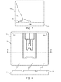
- the silicon nitride layers for the PD barrier and the solder stop areas 30, 32, 34, and 36 are deposited by plasma enhanced chemical vapor deposition (PECVD), and before deposition a mask is placed on the substrate, covering areas of the copper (Cu) metallization where chips, bond wires, pins, terminals, etc. were displaced and no silicon nitride should be deposited.
- PECVD plasma enhanced chemical vapor deposition
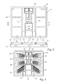
- a RF plasma cleaning process is performed which removes surface contaminants, particles, and activates the surfaces to be coated or covered, and thus increases the adhesion of the silicon nitride film. All edges of the conductive layer 12, as well as parts of the surface of the conductive layer 12 where solder stop areas are to be formed, are covered by depositing a silicon nitride film as shown in Fig. 3 .
- Fig. 3 shows additional areas (not designated by reference signs in Fig. 3 ) which are surrounded by solder stop areas, in particular those in which semiconductor chips 40, 42, 44, 46, 48, and 50 shown in Fig. 4 are to be located.
- Chip assembly follows according to standard processes conventionally used in the semiconductor or microelectronics industry.
- Fig. 4 also shows gate control pins 52, 54 and terminal solder pads 56, 58 of the high power semiconductor device of Fig. 4 .
- pins, terminal contacts, etc. are masked before a second silicon nitride film deposition is performed. Gate, emitter, and collector of the semiconductor chips 40 to 50 are short-circuited to guarantee that they are at the same potential.
- the arrangement shown in Fig. 4 is plasma cleaned and coated with silicon nitride for providing a passivation of the surfaces of the high power semiconductor device of Fig. 4 against corrosion and mechanical damage.
- polyimide PI is deposited thereon as a layer, according to a standard process conventionally employed in the microelectronics or semiconductor industry.
- another ceramic material instead of silicon nitride may be used as the ceramic material for the PD barrier and/or the solder stop area of the high power semiconductor device.
Landscapes
- Internal Circuitry In Semiconductor Integrated Circuit Devices (AREA)
Priority Applications (1)
| Application Number | Priority Date | Filing Date | Title |
|---|---|---|---|
| EP09171605A EP2302676A1 (fr) | 2009-09-29 | 2009-09-29 | Dispositif semi-conducteur haute puissance |
Applications Claiming Priority (1)
| Application Number | Priority Date | Filing Date | Title |
|---|---|---|---|
| EP09171605A EP2302676A1 (fr) | 2009-09-29 | 2009-09-29 | Dispositif semi-conducteur haute puissance |
Publications (1)
| Publication Number | Publication Date |
|---|---|
| EP2302676A1 true EP2302676A1 (fr) | 2011-03-30 |
Family
ID=41428446
Family Applications (1)
| Application Number | Title | Priority Date | Filing Date |
|---|---|---|---|
| EP09171605A Withdrawn EP2302676A1 (fr) | 2009-09-29 | 2009-09-29 | Dispositif semi-conducteur haute puissance |
Country Status (1)
| Country | Link |
|---|---|
| EP (1) | EP2302676A1 (fr) |
Cited By (7)
| Publication number | Priority date | Publication date | Assignee | Title |
|---|---|---|---|---|
| CN103594505A (zh) * | 2013-11-21 | 2014-02-19 | 西安永电电气有限责任公司 | 一种局部放电减弱的高压igbt模块及其制造方法 |
| CN105304619A (zh) * | 2014-05-28 | 2016-02-03 | 株洲南车时代电气股份有限公司 | 一种igbt衬板结构及其制作方法 |
| DE102014115815A1 (de) * | 2014-10-30 | 2016-05-04 | Infineon Technologies Ag | Schaltungsträger, verfahren zur herstellung eines schaltungsträgers, verfahren zur herstellung einer schaltungsanordung, verfahren zum betrieb einer schaltungsanordnung und verfahren zur herstellung eines halbleitermoduls |
| JP2017034075A (ja) * | 2015-07-31 | 2017-02-09 | 富士電機株式会社 | 電子デバイス |
| US9698116B2 (en) | 2014-10-31 | 2017-07-04 | Nxp Usa, Inc. | Thick-silver layer interface for a semiconductor die and corresponding thermal layer |
| DE112015003405B4 (de) * | 2014-07-24 | 2024-03-28 | OSRAM Opto Semiconductors Gesellschaft mit beschränkter Haftung | Träger für ein elektrisches Bauelement und Verfahren zur Herstellung eines Trägers |
| CN118198052A (zh) * | 2024-02-02 | 2024-06-14 | 清华大学 | 电子器件封装模块 |
Citations (9)
| Publication number | Priority date | Publication date | Assignee | Title |
|---|---|---|---|---|
| GB2249670A (en) * | 1990-10-05 | 1992-05-13 | Fuji Electric Co Ltd | Electrical wiring pattern on insulation coated metal substrate |
| GB2268108A (en) * | 1992-06-30 | 1994-01-05 | Hughes Aircraft Co | Electrical interconnection substrate with both wire bond and solder contacts, and fabrication method. |
| EP0921565A2 (fr) * | 1997-12-08 | 1999-06-09 | Kabushiki Kaisha Toshiba | Empaquetage pour dispositif semiconducteur de puissance et procédé pour son assemblage |
| EP0962974A2 (fr) * | 1998-05-28 | 1999-12-08 | Hitachi, Ltd. | Dispositif semi-conducteur |
| JP2002076197A (ja) * | 2000-08-24 | 2002-03-15 | Toshiba Corp | 半導体装置用基板及び半導体装置 |
| EP1321985A1 (fr) * | 2001-12-20 | 2003-06-25 | STMicroelectronics S.r.l. | Transistor à effet de champ de type métal-oxyde-semi-conducteur |
| DE102006004788A1 (de) * | 2005-02-03 | 2006-08-10 | Fuji Electric Device Technology Co. Ltd. | Halbleiterbauelement und Fertigungsverfahren für dieses |
| EP1699080A1 (fr) * | 2005-03-04 | 2006-09-06 | Dowa Mining Co., Ltd. | Substrat en céramique et sa fabrication |
| WO2007012558A1 (fr) * | 2005-07-26 | 2007-02-01 | Siemens Aktiengesellschaft | Ensemble constitue d'un composant electrique et d'un composite a base de films contrecolle sur ce composant et procede de production de cet ensemble |
-
2009
- 2009-09-29 EP EP09171605A patent/EP2302676A1/fr not_active Withdrawn
Patent Citations (9)
| Publication number | Priority date | Publication date | Assignee | Title |
|---|---|---|---|---|
| GB2249670A (en) * | 1990-10-05 | 1992-05-13 | Fuji Electric Co Ltd | Electrical wiring pattern on insulation coated metal substrate |
| GB2268108A (en) * | 1992-06-30 | 1994-01-05 | Hughes Aircraft Co | Electrical interconnection substrate with both wire bond and solder contacts, and fabrication method. |
| EP0921565A2 (fr) * | 1997-12-08 | 1999-06-09 | Kabushiki Kaisha Toshiba | Empaquetage pour dispositif semiconducteur de puissance et procédé pour son assemblage |
| EP0962974A2 (fr) * | 1998-05-28 | 1999-12-08 | Hitachi, Ltd. | Dispositif semi-conducteur |
| JP2002076197A (ja) * | 2000-08-24 | 2002-03-15 | Toshiba Corp | 半導体装置用基板及び半導体装置 |
| EP1321985A1 (fr) * | 2001-12-20 | 2003-06-25 | STMicroelectronics S.r.l. | Transistor à effet de champ de type métal-oxyde-semi-conducteur |
| DE102006004788A1 (de) * | 2005-02-03 | 2006-08-10 | Fuji Electric Device Technology Co. Ltd. | Halbleiterbauelement und Fertigungsverfahren für dieses |
| EP1699080A1 (fr) * | 2005-03-04 | 2006-09-06 | Dowa Mining Co., Ltd. | Substrat en céramique et sa fabrication |
| WO2007012558A1 (fr) * | 2005-07-26 | 2007-02-01 | Siemens Aktiengesellschaft | Ensemble constitue d'un composant electrique et d'un composite a base de films contrecolle sur ce composant et procede de production de cet ensemble |
Non-Patent Citations (1)
| Title |
|---|
| S. M. SZE: "Physics and Technology", 1985, JOHN WILEY & SONS, article "Semiconductor Devices", pages: 360 - 362 |
Cited By (10)
| Publication number | Priority date | Publication date | Assignee | Title |
|---|---|---|---|---|
| CN103594505A (zh) * | 2013-11-21 | 2014-02-19 | 西安永电电气有限责任公司 | 一种局部放电减弱的高压igbt模块及其制造方法 |
| WO2015074431A1 (fr) * | 2013-11-21 | 2015-05-28 | 西安永电电气有限责任公司 | Module igbt haute tension à atténuation de décharge partielle et son procédé de fabrication |
| CN105304619A (zh) * | 2014-05-28 | 2016-02-03 | 株洲南车时代电气股份有限公司 | 一种igbt衬板结构及其制作方法 |
| DE112015003405B4 (de) * | 2014-07-24 | 2024-03-28 | OSRAM Opto Semiconductors Gesellschaft mit beschränkter Haftung | Träger für ein elektrisches Bauelement und Verfahren zur Herstellung eines Trägers |
| DE102014115815A1 (de) * | 2014-10-30 | 2016-05-04 | Infineon Technologies Ag | Schaltungsträger, verfahren zur herstellung eines schaltungsträgers, verfahren zur herstellung einer schaltungsanordung, verfahren zum betrieb einer schaltungsanordnung und verfahren zur herstellung eines halbleitermoduls |
| US9651979B2 (en) | 2014-10-30 | 2017-05-16 | Infineon Technologies Ag | Circuit carrier, method for producing a circuit carrier, method for producing a circuit arrangement, method for operating a circuit arrangement and method for producing a semiconductor module |
| DE102014115815B4 (de) | 2014-10-30 | 2022-11-17 | Infineon Technologies Ag | Verfahren zur herstellung eines schaltungsträgers, verfahren zur herstellung einer halbleiteranordung, verfahren zum betrieb einer halbleiteranordnung und verfahren zur herstellung eines halbleitermoduls |
| US9698116B2 (en) | 2014-10-31 | 2017-07-04 | Nxp Usa, Inc. | Thick-silver layer interface for a semiconductor die and corresponding thermal layer |
| JP2017034075A (ja) * | 2015-07-31 | 2017-02-09 | 富士電機株式会社 | 電子デバイス |
| CN118198052A (zh) * | 2024-02-02 | 2024-06-14 | 清华大学 | 电子器件封装模块 |
Similar Documents
| Publication | Publication Date | Title |
|---|---|---|
| US9673163B2 (en) | Semiconductor device with flip chip structure and fabrication method of the semiconductor device | |
| EP2302676A1 (fr) | Dispositif semi-conducteur haute puissance | |
| US8466007B2 (en) | Power semiconductor module and fabrication method | |
| US20100019381A1 (en) | Semiconductor device and method of manufacturing a semiconductor device | |
| US7659611B2 (en) | Vertical power semiconductor component, semiconductor device and methods for the production thereof | |
| US8164173B2 (en) | Panel, semiconductor device and method for the production thereof | |
| US8310040B2 (en) | Semiconductor device package having high breakdown voltage and low parasitic inductance and method of manufacturing thereof | |
| CN101809770A (zh) | 光电子半导体芯片,光电子器件和用于制造光电子器件的方法 | |
| US9721900B2 (en) | Semiconductor package and its manufacturing method | |
| US9165792B2 (en) | Integrated circuit, a chip package and a method for manufacturing an integrated circuit | |
| US10892253B2 (en) | Semiconductor device manufacturing method and semiconductor device | |
| US8432024B2 (en) | Integrated circuit including bond wire directly bonded to pad | |
| JP6822056B2 (ja) | 半導体装置およびモジュール型半導体装置 | |
| US7368380B2 (en) | Method of manufacturing semiconductor device | |
| CN108346587A (zh) | 芯片封装器件及封装方法 | |
| US8324115B2 (en) | Semiconductor chip, semiconductor device and methods for producing the same | |
| EP2677541A1 (fr) | Méthode pour connecter des fils à une puce semi-conductrice de puissance et le dispositif correspondant | |
| US20080001244A1 (en) | System Comprising an Electrical Component and an Electrical Connecting Lead for Said Component, and Method for the Production of Said System | |
| US10236244B2 (en) | Semiconductor device and production method therefor | |
| JP7138720B2 (ja) | 半導体装置、電力用半導体モジュール、電力変換装置および電力用半導体モジュールの製造方法 | |
| US20130221514A1 (en) | Semiconductor device and fabrication method for the same | |
| US8519547B2 (en) | Chip arrangement and method for producing a chip arrangement | |
| EP1995777A1 (fr) | Paquet de transistor doté d'une isolation diélectrique au niveau de la tranche | |
| US11152286B2 (en) | Power semiconductor module device | |
| JP2020174220A (ja) | 半導体パッケージ |
Legal Events
| Date | Code | Title | Description |
|---|---|---|---|
| PUAI | Public reference made under article 153(3) epc to a published international application that has entered the european phase |
Free format text: ORIGINAL CODE: 0009012 |
|
| AK | Designated contracting states |
Kind code of ref document: A1 Designated state(s): AT BE BG CH CY CZ DE DK EE ES FI FR GB GR HR HU IE IS IT LI LT LU LV MC MK MT NL NO PL PT RO SE SI SK SM TR |
|
| AX | Request for extension of the european patent |
Extension state: AL BA RS |
|
| STAA | Information on the status of an ep patent application or granted ep patent |
Free format text: STATUS: THE APPLICATION IS DEEMED TO BE WITHDRAWN |
|
| 18D | Application deemed to be withdrawn |
Effective date: 20111001 |