EP0963038B1 - Circuit de push-pull réglé par un shunt avec une large gamme des fréquences - Google Patents
Circuit de push-pull réglé par un shunt avec une large gamme des fréquences Download PDFInfo
- Publication number
- EP0963038B1 EP0963038B1 EP99304108A EP99304108A EP0963038B1 EP 0963038 B1 EP0963038 B1 EP 0963038B1 EP 99304108 A EP99304108 A EP 99304108A EP 99304108 A EP99304108 A EP 99304108A EP 0963038 B1 EP0963038 B1 EP 0963038B1
- Authority
- EP
- European Patent Office
- Prior art keywords
- transistor
- circuit
- collector
- srpp
- emitter
- Prior art date
- Legal status (The legal status is an assumption and is not a legal conclusion. Google has not performed a legal analysis and makes no representation as to the accuracy of the status listed.)
- Expired - Lifetime
Links
Images


Classifications
-
- H—ELECTRICITY
- H03—ELECTRONIC CIRCUITRY
- H03F—AMPLIFIERS
- H03F3/00—Amplifiers with only discharge tubes or only semiconductor devices as amplifying elements
- H03F3/30—Single-ended push-pull [SEPP] amplifiers; Phase-splitters therefor
- H03F3/3083—Single-ended push-pull [SEPP] amplifiers; Phase-splitters therefor the power transistors being of the same type
- H03F3/3084—Single-ended push-pull [SEPP] amplifiers; Phase-splitters therefor the power transistors being of the same type one of the power transistors being controlled by the output signal
-
- H—ELECTRICITY
- H03—ELECTRONIC CIRCUITRY
- H03F—AMPLIFIERS
- H03F3/00—Amplifiers with only discharge tubes or only semiconductor devices as amplifying elements
- H03F3/50—Amplifiers in which input is applied to, or output is derived from, an impedance common to input and output circuits of the amplifying element, e.g. cathode follower
Definitions
- the present invention relates to an SRPP circuit (shunt regulated push pull).
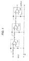
- Fig. 1 of the accompanying drawings shows a case in which a sexinary (six-pole) low-pass filter is formed as an active filter.
- Amplifiers A1 to A3 as used are generally formed of voltage followers.
- the voltage followers A1 to A3 (amplifiers A1 to A3) may be formed of (1) emitter followers, (2) SRPP circuits, (3) operational amplifiers, or the like.
- the emitter follower of (1) may be structured, for example, as shown in Fig. 2. That is, the transistor Q1 has its emitter connected with a constant-current power transistor Q2 to form an emitter follower, its base supplied with an input signal voltage Vin and a base bias voltage VBB and its collector supplied with a supply voltage VCC. In this way, an output voltage or an output current is extracted from the emitter of transistor Q1.
- the emitter current IE1 of the transistor Q1 varies in proportion with a signal voltage Vin with the value IC2 as a centre.
- the amount of variation is extracted as an output.
- an output current as large as desired can be extracted within a range in which the characteristics of the transistor Q1 permit it during a positive half cycle period.
- an output current larger than IC2 cannot be extracted.
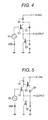
- the SRPP circuit of (2) can be structured as shown in Fig. 4.
- a signal voltage opposite in phase to the input signal voltage Vin is outputted to the collector of the transistor Q1, and the signal voltage is supplied to the base of a transistor Q2 through a capacitor C1. Accordingly, since the transistors Q1 and Q2 are driven with phases opposite to each other, the emitter current of the transistor Q1 and the collector current of the transistor Q2 vary in directions opposite to each other, and the amount of their difference is extracted as the output current. Accordingly, the SRPP circuit can extract a large output current even during the negative half cycle period.
- the SRPP circuit since the base input of the transistor Q2 is supplied from the collector of the transistor Q1 through the capacitor C1 for d.c. cutting, it is necessary to increase the value of the capacitor C1 in order to extract a large output even in a low frequency. Accordingly, the SRPP circuit is not suitable for IC.
- the SRPP circuit shown in Fig. 5 has been proposed. That is, in the SRPP circuit, the collector output of the transistor Q1 is extracted through the transistor Q3 that constitutes the emitter follower, and a d.c. voltage is shifted by a constant voltage diode D1 before being supplied to the base of the transistor Q2.
- DE-A-19 616 443 discloses a shunt regulated push-pull circuit with first and second transistors of the same polarity, the collector of the first transistor being connected to a first reference potential through a resistor and the collector of the second transistor being connected to the emitter of the first transistor.
- the emitter of the second transistor is connected to a second reference potential.
- the circuit further has a third transistor with opposite polarity to that of the first and second, its emitter connected to the collector of the first transistor, its collector connected to the base of the second transistor and a bias voltage being supplied to its base.
- An input signal is supplied to the base of the first transistor and an output is extracted from a node of the emitter of the first transistor and the collector of the second transistor.
- the present invention has been made to reduce or eliminate te above problems with the conventional circuit.
- SRPP circuit Shunt Regulated Push-Pull circuit
- the third transistor since the third transistor operates with its base being grounded to supply the collector output of the first transistor to the base of the second transistor, the above circuit structure operates as an SRPP circuit.
- a transistor Q11 has a base to which an input signal voltage Vin and a base bias voltage V11 are applied, and a collector connected to a first reference potential point, for example, a power supply terminal T13 through a resistor R11.
- the transistor Q11 also has an emitter connected to the collector of a transistor Q12 having the same polarity as that of the transistor Q11, and the emitter of the transistor Q12 is connected to a second reference potential point, for example, the ground.
- the collector of the transistor Q11 is connected to the emitter of a transistor Q13 having the polarity opposite to that of the transistor Q11, and the collector of the transistor Q13 is connected to the base of the transistor Q12.
- the emitter of the transistor Q11 is connected to an output terminal T12
- a capacitor C11 is connected between the emitter and collector of the transistor Q13
- a bias voltage V13 with the power supply terminal T13 as a reference potential point is applied to the base of the transistor Q13.
- the emitter current IE11 of the transistor Q11 increases, and in this situation, the collector current of the transistor Q11 also increases to lower the collector potential thereof.
- the collector current IC12 of the transistor Q12 increases. Therefore, a current which is a difference between an increased amount of the emitter current IE11 and a decreased amount of the collector current IC12 flows out to the terminal T12.
- the emitter current IE11 of the transistor Q11 decreases.
- the collector current of the transistor Q11 also decreases to increase the collector potential thereof.
- the collector current IC12 of the transistor Q12 also increase. Therefore, a current which is a difference between a decreased amount of the emitter current IE11 and an increased amount of the collector current IC12 flows out to the terminal T12.
- the transistor Q13 operates with the base thereof being grounded in response to the collector output of the transistor Q11, and the collector output is supplied to the base of the transistor Q12 in the same phase.
- the input signal voltage Vin is opposite in phase to the collector output of the transistor Q11. Accordingly, the transistors Q11 and Q12 are driven with the phases opposite to each other with respect to the signal voltage Vin, to thereby execute the SRPP operation.
- the transistor Q13 since the transistor Q13 operates with its base being grounded, the frequency characteristic is excellent, and a large output can be obtained from d.c. up to a high frequency.
- the capacitor C11 when the capacitor C11 is connected to the transistor Q13, since the deterioration of the characteristies of the transistor Q13 in a higher frequency can be compensated, a large output can be obtained up to a higher frequency.
- the capacitor C11 since the capacitor C11 is provided for compensation in the high frequency, its value may be set at about 1 to 3 pF, and the entire circuit can be put into an IC without problems.
- the circuit is applicable in a range of a wide supply voltage VCC. Also, since the number of elements as required is small, even in the case where the circuit is applied to a high-degree active filter, the circuit scale is not increased. Further, since the frequency characteristic is excellent as described above, the circuit is also applicable to an active filter adapted to a high frequency without problems.
- the circuit is suitable as the voltage follower in the active filter.
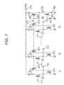
- Fig. 7 shows an embodiment of a bias circuit designed in such a manner that a bias voltage V13 can be applied to the above-described N SRPP circuits, in which reference symbols 11 to 1N denote the respective SRPP circuits described above. It should be noted that those SRPP circuits 11 to 1N are not connected to the capacitor C11 for improvement of a high-frequency characteristic for simplification of the figure, but the former may be connected to the latter.
- a transistor Q21 has a base to which a given bias voltage V21 is applied, an emitter grounded through a resistor R21 and a collector connected to the collector and the base of the transistor Q22.
- the transistor Q22 structures a current mirror circuit 22 in which the transistor Q21 is disposed at an input side and the transistors Q13 to Q13 of the SRPP circuits 11 to 1N are disposed at an output side.
- the base of the transistor Q22 is connected to the bases of the transistors Q13 to Q13, and the emitter of the transistor Q22 is connected to the power supply terminal T13 through a resistor R22.
- the base voltage that supplies the base current IB22 to the transistor Q22 is also applied to the bases of the transistors Q13 to Q13. Accordingly, the bias voltage V13 is applied to the transistors Q13 to Q13.
- the bias voltage V13 can be applied to N SRPP circuits 11 to 1N with an extremely simple structure as is apparent from the drawing. Also, since the transistors Q13 to Q13 operate with their bases being grounded and the base currents of the transistors Q13 to Q13 are extremely small, even if the bias voltage V13 is applied commonly to the bases of the transistors Q13 to Q13, an interference between the SRPP circuits 11 to 1N can be sufficiently reduced.
- a large output can be obtained within a range in which the output is permitted by the characteristics of the transistors Q11 and Q12, and in this situation, there is no case in which the output current during one half cycle is limited.
- the frequency characteristic is excellent, and a large output can be obtained from d.c. even in a high frequency.
- a large output can be obtained up to a higher frequency. Then, since the capacitor C11 is provided for compensation' in a high frequency in this case, the value of the capacitor C11 may be small, and even if the capacitor C11 is connected in the circuit, the entire circuit can be put into an IC without problems.
- the circuit can be used within a range of a wide supply voltage. Also, since the number of elements as required is small, even in the case where the circuit is used in a high-degree active filter, the circuit scale does not become larger. In addition, since the output impedance is low and a change in the output impedance due to the signal frequency is small, the circuit is suitable, for example, as the voltage follower in the active filter.
- the bias circuit can be structured very simply. Also, even when the bias voltage is applied commonly to a plurality of SRPP circuits, an interference between the respective SRPP circuits can be sufficiently reduced.
Landscapes
- Engineering & Computer Science (AREA)
- Power Engineering (AREA)
- Amplifiers (AREA)
- Networks Using Active Elements (AREA)
- Radar Systems Or Details Thereof (AREA)
Claims (5)
- Circuit push-pull réglé par un shunt (circuit SRPP) comprenant :dans lequel un signal d'entrée (Vin) est transmis à la base dudit premier transistor (Q11) et un signal de sortie est extrait d'un noeud présent entre l'émetteur dudit premier transistor et le collecteur dudit deuxième transistor (Q12) ;un premier transistor (Q11) ;une résistance (R11) par le biais de laquelle le collecteur dudit premier transistor est connecté à un premier point de potentiel de référence (T13);un deuxième transistor (Q12) ayant la même polarité que celle dudit premier transistor (Q11), le collecteur dudit deuxième transistor étant connecté à l'émetteur dudit premier transistor, l'émetteur dudit deuxième transistor étant connecté à un deuxième point de potentiel de référence ; etun troisième transistor (Q13) ayant une polarité opposée à celle dudit premier transistor (Q11), l'émetteur dudit troisième transistor étant connecté au collecteur dudit premier transistor et le collecteur dudit troisième transistor étant connecté à la base dudit deuxième transistor (Q12), une tension de polarisation étant appliquée à la base dudit troisième transistor ;
caractérisé en ce que le circuit SRPP comprend en outre un condensateur (C11) connecté en parallèle entre l'émetteur et le collecteur dudit troisième transistor (Q13). - Circuit SRPP selon la revendication 1, dans lequel la totalité du circuit SRPP est conçue sous la forme d'un circuit intégré monoboítier.
- Circuit SRPP selon la revendication 1 ou 2, dans lequel ladite tension de polarisation est appliquée à partir d'un circuit de polarisation qui absorbe une modification des caractéristiques des éléments du circuit SRPP.
- Circuit SRPP selon la revendication 3, dans lequel ledit circuit de polarisation est construit à partir d'un circuit à miroir de courant (22).
- Circuit SRPP selon la revendication 3 ou 4, dans lequel la totalité du circuit SRPP est conçue pour s'intégrer à l'intérieur d'un circuit intégré monoboítier.
Applications Claiming Priority (2)
| Application Number | Priority Date | Filing Date | Title |
|---|---|---|---|
| JP15088498 | 1998-06-01 | ||
| JP10150884A JPH11346125A (ja) | 1998-06-01 | 1998-06-01 | Srpp回路 |
Publications (3)
| Publication Number | Publication Date |
|---|---|
| EP0963038A2 EP0963038A2 (fr) | 1999-12-08 |
| EP0963038A3 EP0963038A3 (fr) | 2000-05-17 |
| EP0963038B1 true EP0963038B1 (fr) | 2005-01-19 |
Family
ID=15506496
Family Applications (1)
| Application Number | Title | Priority Date | Filing Date |
|---|---|---|---|
| EP99304108A Expired - Lifetime EP0963038B1 (fr) | 1998-06-01 | 1999-05-26 | Circuit de push-pull réglé par un shunt avec une large gamme des fréquences |
Country Status (6)
| Country | Link |
|---|---|
| US (1) | US6392454B1 (fr) |
| EP (1) | EP0963038B1 (fr) |
| JP (1) | JPH11346125A (fr) |
| KR (1) | KR100646026B1 (fr) |
| CN (1) | CN1111946C (fr) |
| DE (1) | DE69923254T2 (fr) |
Families Citing this family (6)
| Publication number | Priority date | Publication date | Assignee | Title |
|---|---|---|---|---|
| JPH11346125A (ja) * | 1998-06-01 | 1999-12-14 | Sony Corp | Srpp回路 |
| US6492870B2 (en) | 2001-01-11 | 2002-12-10 | Texas Instruments Incorporated | Class AB, high speed, input stage with base current compensation for fast settling time |
| AU2002313702A1 (en) * | 2001-07-24 | 2003-02-17 | Cargill, Incorporated | Process for isolating phenolic compounds |
| US7256654B2 (en) | 2005-04-12 | 2007-08-14 | Raytheon Company | Amplifying a signal using a current shared power amplifier |
| CN109075756B (zh) * | 2016-03-31 | 2022-06-07 | 日本电信电话株式会社 | 驱动电路和光发射器 |
| CN116243755B (zh) * | 2023-05-09 | 2023-07-25 | 国仪量子(合肥)技术有限公司 | 数据采集装置和数据采集与监控系统 |
Citations (1)
| Publication number | Priority date | Publication date | Assignee | Title |
|---|---|---|---|---|
| DE19616443A1 (de) * | 1996-04-25 | 1997-10-30 | Cafer Borucu | Gegentakt-Endstufe für analoge und digitale Schaltungen |
Family Cites Families (11)
| Publication number | Priority date | Publication date | Assignee | Title |
|---|---|---|---|---|
| JPS5330212Y2 (fr) * | 1972-09-22 | 1978-07-28 | ||
| US4017788A (en) | 1975-11-19 | 1977-04-12 | Texas Instruments Incorporated | Programmable shunt voltage regulator circuit |
| JPS60145784A (ja) | 1984-01-09 | 1985-08-01 | Hitachi Ltd | インデツクス方式カラ−画像再生装置 |
| JPS60223381A (ja) | 1984-04-20 | 1985-11-07 | Hitachi Ltd | 走査速度変調回路 |
| JPS6417505A (en) * | 1987-07-13 | 1989-01-20 | Hitachi Ltd | Srpp system video output circuit |
| JPH0793687B2 (ja) | 1988-04-11 | 1995-10-09 | 株式会社日立製作所 | 垂直偏向回路 |
| US4879506A (en) | 1988-08-02 | 1989-11-07 | Motorola, Inc. | Shunt regulator |
| DE4321483C2 (de) * | 1993-06-28 | 1995-04-20 | Siemens Ag | Leitungstreiberschaltstufe in Stromschaltertechnik |
| JPH08228136A (ja) | 1995-02-21 | 1996-09-03 | Oki Electric Ind Co Ltd | トランジスタスイッチング回路 |
| JP3707212B2 (ja) * | 1997-09-19 | 2005-10-19 | ソニー株式会社 | パルス出力回路 |
| JPH11346125A (ja) * | 1998-06-01 | 1999-12-14 | Sony Corp | Srpp回路 |
-
1998
- 1998-06-01 JP JP10150884A patent/JPH11346125A/ja active Pending
-
1999
- 1999-05-25 US US09/317,832 patent/US6392454B1/en not_active Expired - Fee Related
- 1999-05-26 DE DE69923254T patent/DE69923254T2/de not_active Expired - Fee Related
- 1999-05-26 EP EP99304108A patent/EP0963038B1/fr not_active Expired - Lifetime
- 1999-05-28 KR KR1019990019411A patent/KR100646026B1/ko not_active Expired - Fee Related
- 1999-05-31 CN CN99109260A patent/CN1111946C/zh not_active Expired - Fee Related
Patent Citations (1)
| Publication number | Priority date | Publication date | Assignee | Title |
|---|---|---|---|---|
| DE19616443A1 (de) * | 1996-04-25 | 1997-10-30 | Cafer Borucu | Gegentakt-Endstufe für analoge und digitale Schaltungen |
Also Published As
| Publication number | Publication date |
|---|---|
| JPH11346125A (ja) | 1999-12-14 |
| CN1244067A (zh) | 2000-02-09 |
| DE69923254T2 (de) | 2005-12-29 |
| KR100646026B1 (ko) | 2006-11-13 |
| EP0963038A3 (fr) | 2000-05-17 |
| US6392454B1 (en) | 2002-05-21 |
| EP0963038A2 (fr) | 1999-12-08 |
| DE69923254D1 (de) | 2005-02-24 |
| KR20000005731A (ko) | 2000-01-25 |
| CN1111946C (zh) | 2003-06-18 |
Similar Documents
| Publication | Publication Date | Title |
|---|---|---|
| US6342815B1 (en) | Manufacturable HBT power distributed amplifier for wideband telecommunications | |
| US6147552A (en) | Chopper-stabilized operational amplifier including integrated circuit with true random voltage output | |
| US7365604B2 (en) | RF amplifier with a bias boosting scheme | |
| KR100194311B1 (ko) | 고이득 증폭 회로 | |
| US6064257A (en) | Chopper-stabilized operational amplifier | |
| JP2005512376A (ja) | 電流ミラー回路を使用するバイアス補償を有する増幅器 | |
| US4906869A (en) | Output circuit having wide range frequency response characteristic | |
| US5751190A (en) | Gain-controlled amplifier and distributed amplifier | |
| KR100269007B1 (ko) | 증폭회로 | |
| US4956615A (en) | Input circuit for high-frequency amplifiers | |
| EP0963038B1 (fr) | Circuit de push-pull réglé par un shunt avec une large gamme des fréquences | |
| KR850001539B1 (ko) | 전류형 4차 능동여파기 | |
| US4518930A (en) | Negative resistance circuit for VCO | |
| US4540953A (en) | Gain control circuit for obtaining a constant output signal amplitude by attenuating an input signal amplitude | |
| US4460876A (en) | Low consumption, wide-band linear amplifier operating in sliding class A | |
| US5721484A (en) | Power supply filter with active element assist | |
| KR19980018571A (ko) | 전자 회로 및 저항기 네트워크 | |
| US5262690A (en) | Variable delay clock circuit | |
| US6002296A (en) | Filter circuit with an intermittent constant current with constant period | |
| US6218906B1 (en) | Amplifier circuit | |
| JPH01236811A (ja) | 高周波発振器 | |
| US5986511A (en) | Frequency dependent impedance | |
| US3422365A (en) | Stabilized transistor amplifier | |
| US5218323A (en) | Transistor direct-coupled amplifier | |
| KR100197842B1 (ko) | 가변 리액턴스 회로 |
Legal Events
| Date | Code | Title | Description |
|---|---|---|---|
| PUAI | Public reference made under article 153(3) epc to a published international application that has entered the european phase |
Free format text: ORIGINAL CODE: 0009012 |
|
| AK | Designated contracting states |
Kind code of ref document: A2 Designated state(s): DE FR GB |
|
| AX | Request for extension of the european patent |
Free format text: AL;LT;LV;MK;RO;SI |
|
| RIC1 | Information provided on ipc code assigned before grant |
Free format text: 7H 03F 3/26 A, 7H 02M 3/337 B, 7G 05F 1/59 B, 7G 05F 3/22 B, 7H 02M 3/158 B |
|
| PUAL | Search report despatched |
Free format text: ORIGINAL CODE: 0009013 |
|
| AK | Designated contracting states |
Kind code of ref document: A3 Designated state(s): AT BE CH CY DE DK ES FI FR GB GR IE IT LI LU MC NL PT SE |
|
| AX | Request for extension of the european patent |
Free format text: AL;LT;LV;MK;RO;SI |
|
| 17P | Request for examination filed |
Effective date: 20001020 |
|
| AKX | Designation fees paid |
Free format text: DE FR GB |
|
| 17Q | First examination report despatched |
Effective date: 20040309 |
|
| GRAP | Despatch of communication of intention to grant a patent |
Free format text: ORIGINAL CODE: EPIDOSNIGR1 |
|
| GRAS | Grant fee paid |
Free format text: ORIGINAL CODE: EPIDOSNIGR3 |
|
| GRAA | (expected) grant |
Free format text: ORIGINAL CODE: 0009210 |
|
| AK | Designated contracting states |
Kind code of ref document: B1 Designated state(s): DE FR GB |
|
| REG | Reference to a national code |
Ref country code: GB Ref legal event code: FG4D |
|
| REF | Corresponds to: |
Ref document number: 69923254 Country of ref document: DE Date of ref document: 20050224 Kind code of ref document: P |
|
| PLBE | No opposition filed within time limit |
Free format text: ORIGINAL CODE: 0009261 |
|
| STAA | Information on the status of an ep patent application or granted ep patent |
Free format text: STATUS: NO OPPOSITION FILED WITHIN TIME LIMIT |
|
| ET | Fr: translation filed | ||
| 26N | No opposition filed |
Effective date: 20051020 |
|
| PGFP | Annual fee paid to national office [announced via postgrant information from national office to epo] |
Ref country code: DE Payment date: 20080529 Year of fee payment: 10 |
|
| PGFP | Annual fee paid to national office [announced via postgrant information from national office to epo] |
Ref country code: GB Payment date: 20080528 Year of fee payment: 10 |
|
| GBPC | Gb: european patent ceased through non-payment of renewal fee |
Effective date: 20090526 |
|
| REG | Reference to a national code |
Ref country code: FR Ref legal event code: ST Effective date: 20100129 |
|
| PG25 | Lapsed in a contracting state [announced via postgrant information from national office to epo] |
Ref country code: FR Free format text: LAPSE BECAUSE OF NON-PAYMENT OF DUE FEES Effective date: 20090602 |
|
| PGFP | Annual fee paid to national office [announced via postgrant information from national office to epo] |
Ref country code: FR Payment date: 20080514 Year of fee payment: 10 |
|
| PG25 | Lapsed in a contracting state [announced via postgrant information from national office to epo] |
Ref country code: GB Free format text: LAPSE BECAUSE OF NON-PAYMENT OF DUE FEES Effective date: 20090526 |
|
| PG25 | Lapsed in a contracting state [announced via postgrant information from national office to epo] |
Ref country code: DE Free format text: LAPSE BECAUSE OF NON-PAYMENT OF DUE FEES Effective date: 20091201 |