EP0963101A2 - Bildsensormodul mit sechs Freiheitsgraden für den Gebrauch zusammen mit einer Bilderfassungsvorrichtung - Google Patents
Bildsensormodul mit sechs Freiheitsgraden für den Gebrauch zusammen mit einer Bilderfassungsvorrichtung Download PDFInfo
- Publication number
- EP0963101A2 EP0963101A2 EP99201701A EP99201701A EP0963101A2 EP 0963101 A2 EP0963101 A2 EP 0963101A2 EP 99201701 A EP99201701 A EP 99201701A EP 99201701 A EP99201701 A EP 99201701A EP 0963101 A2 EP0963101 A2 EP 0963101A2
- Authority
- EP
- European Patent Office
- Prior art keywords
- image sensor
- sensor array
- base plate
- optical system
- module
- Prior art date
- Legal status (The legal status is an assumption and is not a legal conclusion. Google has not performed a legal analysis and makes no representation as to the accuracy of the status listed.)
- Withdrawn
Links
Images




Classifications
-
- H—ELECTRICITY
- H04—ELECTRIC COMMUNICATION TECHNIQUE
- H04N—PICTORIAL COMMUNICATION, e.g. TELEVISION
- H04N1/00—Scanning, transmission or reproduction of documents or the like, e.g. facsimile transmission; Details thereof
- H04N1/024—Details of scanning heads ; Means for illuminating the original
- H04N1/028—Details of scanning heads ; Means for illuminating the original for picture information pick-up
- H04N1/03—Details of scanning heads ; Means for illuminating the original for picture information pick-up with photodetectors arranged in a substantially linear array
-
- H—ELECTRICITY
- H04—ELECTRIC COMMUNICATION TECHNIQUE
- H04N—PICTORIAL COMMUNICATION, e.g. TELEVISION
- H04N2201/00—Indexing scheme relating to scanning, transmission or reproduction of documents or the like, and to details thereof
- H04N2201/024—Indexing scheme relating to scanning, transmission or reproduction of documents or the like, and to details thereof deleted
- H04N2201/02406—Arrangements for positioning elements within a head
- H04N2201/02416—Rotational positioning, i.e. with respect to an axis
- H04N2201/02418—Rotation about the optical axis
-
- H—ELECTRICITY
- H04—ELECTRIC COMMUNICATION TECHNIQUE
- H04N—PICTORIAL COMMUNICATION, e.g. TELEVISION
- H04N2201/00—Indexing scheme relating to scanning, transmission or reproduction of documents or the like, and to details thereof
- H04N2201/024—Indexing scheme relating to scanning, transmission or reproduction of documents or the like, and to details thereof deleted
- H04N2201/02406—Arrangements for positioning elements within a head
- H04N2201/02416—Rotational positioning, i.e. with respect to an axis
- H04N2201/0242—Rotation about an axis in the plane of the scanning elements orthogonal to the optical axis, the axis of rotation extending in the main-scanning direction, e.g. the longitudinal axis of a linear array
-
- H—ELECTRICITY
- H04—ELECTRIC COMMUNICATION TECHNIQUE
- H04N—PICTORIAL COMMUNICATION, e.g. TELEVISION
- H04N2201/00—Indexing scheme relating to scanning, transmission or reproduction of documents or the like, and to details thereof
- H04N2201/024—Indexing scheme relating to scanning, transmission or reproduction of documents or the like, and to details thereof deleted
- H04N2201/02406—Arrangements for positioning elements within a head
- H04N2201/02416—Rotational positioning, i.e. with respect to an axis
- H04N2201/02422—Rotation about an axis in the plane of the scanning elements orthogonal to the optical axis, the axis of rotation extending in the sub-scanning direction, e.g. the transverse axis of a linear array
-
- H—ELECTRICITY
- H04—ELECTRIC COMMUNICATION TECHNIQUE
- H04N—PICTORIAL COMMUNICATION, e.g. TELEVISION
- H04N2201/00—Indexing scheme relating to scanning, transmission or reproduction of documents or the like, and to details thereof
- H04N2201/024—Indexing scheme relating to scanning, transmission or reproduction of documents or the like, and to details thereof deleted
- H04N2201/02406—Arrangements for positioning elements within a head
- H04N2201/02427—Element positioned
- H04N2201/02429—Photodetector element, e.g. CCD array
-
- H—ELECTRICITY
- H04—ELECTRIC COMMUNICATION TECHNIQUE
- H04N—PICTORIAL COMMUNICATION, e.g. TELEVISION
- H04N2201/00—Indexing scheme relating to scanning, transmission or reproduction of documents or the like, and to details thereof
- H04N2201/024—Indexing scheme relating to scanning, transmission or reproduction of documents or the like, and to details thereof deleted
- H04N2201/02406—Arrangements for positioning elements within a head
- H04N2201/02439—Positioning method
- H04N2201/02441—Positioning method using screws
-
- H—ELECTRICITY
- H04—ELECTRIC COMMUNICATION TECHNIQUE
- H04N—PICTORIAL COMMUNICATION, e.g. TELEVISION
- H04N2201/00—Indexing scheme relating to scanning, transmission or reproduction of documents or the like, and to details thereof
- H04N2201/04—Scanning arrangements
- H04N2201/047—Detection, control or error compensation of scanning velocity or position
- H04N2201/04753—Control or error compensation of scanning position or velocity
- H04N2201/04794—Varying the control or compensation during the scan, e.g. using continuous feedback or from line to line
- H04N2201/04796—Varying the sub-scan control during the main-scan, e.g. for correcting skew, tilt or bow of a scanning beam
Definitions
- Digital image acquisition devices e.g. , scanners, digital copiers, and digital cameras, are used to digitize the graphic content, be it color or black and white photographs, artwork, text, and other graphics, from reflective and/or transmissive original documents.
- This capability is useful in digital document storage, digital content generation, and in more industrial pre-process environments, In this latter implementation, chemical film-based photographs, for example, can be digitally scanned for pre-print review, followed by production printing.
- one of the most common configurations is the flat-bed scanner.
- a transmissive or reflective original document is placed face down on a bed having a glass plate.
- a carriage, under the glass plate, with a slit aperture facing the document, is then scanned over the original document.
- An optical system in the carriage successively picks-off scan lines.
- a single fold mirror is used in a high-resolution mode, and a series of larger fold mirrors are used in a low-resolution mode.
- the fold mirror(s) relay the scanned lines to high or low resolution imaging lens, also of the optical system, which image the scan lines onto a linear or two dimensional image sensor.
- the image sensor is a trilinear charge-coupled device (CCD) array, although newer CMOS-based image sensors are becoming increasingly popular.
- CCD charge-coupled device
- Calibration is a substantial cost factor in the manufacture of scanners and other image acquisition devices.
- the carriage's optical system including the slit aperture, relay optics, and imaging optics, must be aligned to the image sensor array so that an image of the scan line is properly formed on the sensor array.
- the optical system calibration must be robust. After manufacture, these devices are many times transferred by commercial shippers around the world where exposure to shock and temperature extremes take place.
- the most common calibration technique in a scanner involves attaching a prealigned CCD sensor array to the carriage.
- the relay optics and imaging optics are then finely tuned to the required level of alignment with the attached sensor array.
- in-field re-calibration and/or image sensor array replacement/upgrading is very difficult. It is not uncommon for the sensor arrays to fail in the field. The cause can be related to shipment, normal operation, or electrical surge damage. Additionally, the image sensors are sometimes replaced to increase the scanner's resolution as higher density sensors become available and cost-effective. In these situations, the optics in conventional systems must be re-calibrated since the new image sensor array cannot be attached to the carriage in exactly the same orientation as the old sensor. Without proper calibration, the increase in resolution achievable by a new image sensor, for example, may not be realized because of poor image formation on the device. Calibration in the field, however, is even more difficult due to the unavailability of the special-purpose equipment and jigs used to facilitate calibration in the production environment.
- the principles of the present invention are directed towards any image acquisition device, such as a scanner, digital copier, or digital camera.
- the device comprises an image sensor array that detects light imaged by an optical system and an image sensor module that enables calibration of the position of the image sensor array relative to the optical system.
- the module enables alignment of the image sensor array to the optical system.
- the sensor module is separately calibrated to defined standards, making the optical system's calibration independent of the specific module and the module's calibration independent of the specific optical system used in a given image acquisition device.
- the module enables positioning of the sensor array with six degrees of freedom, allowing it to be aligned completely independently of the optical system.
- the electronic circuit board, on which the sensor array is integrated is separate from the motherboard, on which the analog to digital converters are located. This has the advantage of enabling replacement of the analog to digital converters, a primary source of improper operation in the electronic components, without requiring the replacement of the expensive optical sensor array, coupled with the difficulty of re-alignment.
- the invention features an image sensor module for an image acquisition device.
- the module comprises a base plate that is adapted to be mounted to an optical system, and specifically the carriage.
- An image sensor mounting bracket is adapted to carry the image sensor array.
- the mounting bracket is positionable relative to the base plate to enable alignment of the image sensor array to the optical system.
- the mounting bracket is adjustable relative to the base plate in three degrees of freedom. Specifically, it is translationally adjustable along a z-axis, which is defined as being orthogonal to the image plane of the image sensor array; rotationally adjustable relative to a y-axis, which is defined as running parallel to a longitudinal axis of the image sensor array; and rotationally adjustable relative to an x-axis, which is defined as running parallel to a transverse axis of the image sensor array.
- a bracket position alignment system comprises at least one support pin for preloading the mounting bracket relative to the base plate and at least one set screw for controlling a distance between the mounting bracket and a base plate.
- two support pins are used for preloading, and three set screws are used for distance control between the bracket and base plate.
- a base plate position alignment system enables the base plate, and thus the image sensor array, to be oriented relative to the optical system.
- the base plate alignment system provides the three additional degrees of freedom.
- the base plate is translationally adjustable relative to the optical system along the y-axis, rotationally adjustable relative to the z-axis, and translationally adjustable relative to the x-axis.
- the base plate position alignment system in combination with the bracket position alignment system provide a total of six discrete degrees of freedom in the positioning of the sensor array relative to the optical system.
- the sensor array is bonded to the image sensor mounting bracket.
- a daughterboard supporting the analog signal processing of the signals from the sensor array and sampling control for the array, is provided on a daughter card that is supported by the image sensor array.
- the analog to digital converters that digitize these signals from the sensor array are located on a separate motherboard, connected to the daughterboard by a shielded jumper. This enables the replacement of the motherboard with its analog to digital converters without necessitating the removal or replacement of the daughterboard, which must be aligned to the optical system and contains the expensive sensor array.
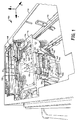
- Fig. 1 shows the main components of a flat-bed scanner 100 incorporating the principles of the present invention.
- the scanner 100 comprises a housing or frame 110. Secured to the housing 110 and extending longitudinally or in the direction parallel to the z-axis are two rails 112, Only the right rail is actually shown due to the perspective. These rails 112 support an optical system carriage 114 that picks-off scan lines s extending in the direction of the y-axis while scanning or traveling in the z-axis.
- An illuminator 116 is installed on the carriage 114.
- a reflector system 118 is used to concentrate light from the illuminator 116 on the original document to be scanned.
- the reflectors are movable between two positions depending upon whether or not a reflective or transmissive original is being scanned. In either case, light from the scanned lines s passes into the carriage through a slit aperture 120.
- relay optics 122 and imaging optics 124 Housed within the carriage are relay optics 122 and imaging optics 124.
- two imaging lens systems are provided 126, 128. They are movable alternatively into the optical path to provide for high or low resolution scanning.
- An image sensor module 130 is secured to the front face 132 of the carriage 114 by three bolts 320, 322, 324. This module 130 carries the image sensor array 134/sensor daughterboard 136.
- the sensor module 130 comprises an image sensor mounting bracket 140 and base plate 142.
- the daughterboard 136 carries the electronics needed to control the image sensor array and to amplify the analog pixel information.
- the analog signals generated by the sensor array are not digitized on the daughterboard 136. Instead they are transferred via a metal shielded jumper 144 to a motherboard 146.
- the motherboard houses the analog to digital converters necessary to digitize the analog signals representing the scanned images from the image sensor array 134.
- the advantage of the separation of the analog to digital converters on the motherboard 146 with the image sensor array on a daughterboard 136 is that the analog to digital converters are replaceable without requiring removal of the image sensor array 134.
- Past experience has demonstrated that the analog to digital converters need to be replaced relatively frequently because of electronic problems. In this configuration, they are replaceable without requiring the removal of the expensive tri-linear CCD array 134 or its realignment.
- Fig. 2 shows the internal arrangement of the optical system carriage.
- reflectors 118 configured for transparent original scanning, surround the illuminator 116 to direct the light through the original ⁇ to slit aperture 120.
- the light is passed to relay optics 122, which direct the light to imaging optics 124.
- the imaging optics 124 form an image of the scan line s on the image sensor array 134 held on the module 130.
- two sets of relay optics are used. Specifically, a single fold mirror 150 is moved into the optical path for high-resolution scanning. During low-resolution scanning. the fold mirror 150 is brought out of the optical path so that the light travels to the low-resolution fold mirrors 154 and 156. The light reflects off the fold mirror 154 to the fold mirror 156 which re-directs the light to the imaging optics 124.
- Fig. 3 is a detailed perspective view of the image sensor module 130 according to the present invention.
- the base plate 142 is essentially rectangular. It supports the image sensor mounting bracket 140 by two pins 160, 162, which provide preloading between the bracket 140 and the base plate 142.
- a bracket position alignment system comprises three bracket set screws 164, 166, 168. These hardened ball tipped set screws 164, 166, 168 engage threads in the bracket 140, project perpendicularly away from rear face of the bracket, and extend through the daughterboard 136, to engage the front face of the base plate 142.
- set screws 164, 166, 168 of the bracket position alignment system By adjustment of the set screws 164, 166, 168 of the bracket position alignment system, the distance between the bracket 140 and the base plate 142 is controlled at three locations. In total, this provides adjustment of the sensor array 134 in three degrees of freedom.
- set screws 164 and 166 are used together to translate the sensor array 134 along the z-axis, which is defined as being orthogonal to the image plane of the image sensor array 134.
- Set screws 164, 166 are adjusted individually or counter to each other to rotate the image sensor array relative to the x-axis.
- the x-axis is defined as running parallel to the transverse axis of the image sensor array 134.
- set screw 168 is used to adjust the rotation of the image sensor array relative to a y-axis.
- the y-axis is defined as running parallel to a longitudinal axis of the image sensor array 134.
- Fig. 3 further shows a base plate position alignment system comprising dog-point set screws 170, 172, 174.
- the base plate set screws 170, 172, 174 mate with threads tapped at 45° through the corners of the base plate 142.
- the base plate alignment system provides three additional degrees of freedom in the positioning of the sensor array 134 by enabling adjustment of the base plate in a mount on the carriage 114.
- adjustment of plate set screws 172 and 170 together provide for translational adjustment of the base plate 142 in the mount along the x-axis.
- the adjustment of set screws 170 or 172 either counter to each other or individually rotate the base plate around the z-axis.
- adjustment of set screw 174 provides for translational adjustment along the y-axis.
- Fig. 4 is another perspective view of the sensor module 130 showing its rear face. This view best shows the CCD array 134 and its position within an aperture 182 in the center of the base plate 142.
- Fig. 5 is an exploded view of the module 130. This view shows the method by which the sensor array 134 is installed on the daughterboard 136. Specifically, its pins 190 extend through holes 192 in the daughterboard 136 to provide mechanical and electrical mating between the sensor array and daughterboard as is convention for chip-to-circuit board connection. Distinguishing the arrangement is the fact that the 142. This allows for expansion and contraction to take place between the bracket 140 and the base plate 142.
- the bracket 140 and base plate 142 are both constructed from die-cast aluminum, and consequently, have the same coefficients of thermal expansion, they are sometimes exposed to different thermal gradients depending due to heat dissipation through the sensor array 134 and daughterboard 136, causing one to expand and contract more than the other. Such thermal expansion and contraction is accommodated in the junction between the bracket 140 and the base plate 142 by allowing set screw 164 to smoothly travel in the V of the set screw engagement region 202.
- set screw engagement region 206 has a flat hardened surface. Since the combination of the cone indent in engagement region 204 and the V of engagement region 202, the movement of the bracket is restricted to y-axis movement. Therefore, region 206 is flat to accommodate this relative movement.
- Fig. 7 is a perspective view showing the front side of the sensor bracket 140. This view shows the ball tips 212 on the bracket set screws 164, 166, 168. Additionally, it shows the block 194 to which the sensor array 134 is bonded.
- Fig. 8 is a perspective view showing the carriage 114 and the mounting area 300 for the module 130.
- the three holes 304, 306, 308 are formed in the frame 290 of the carriage 114. This allows the module 130 to be bolted to the carriage 114 by the three module bolts 320, 322, 324 (shown in Fig. 1).
- three engagement surfaces 310, 312, 314. These form part of the base plate position alignment system. Specifically, the dog-point of base plate adjustment screw 174 engages surface 314, base set screw 172 engages surface 312, and base set screw 170 engages surface 310.
- the set screws are locked from moving out of adjustment by a screw sealant such as VIBRA-TITETM sold by ND Industries.
- sensor array 134 is then bonded to block 194, which is integral with the image sensor mounting bracket 140.
- the daughterboard 136 is actually mechanically supported by the sensor chip. In this way, the sensor array 134 is directly attached to the rigid metal bracket 140.
- the sensor arrays were supported by the daughterboard. This subjected alignment to any mechanical instabilities associated with daughterboard.
- the direct bonding of the CCD array to the metal bracket avoids these variables in the preferred embodiment.
- curved washers 198, 200 that are installed on the shafts of the preload pins 160, 162, respectively, between the head of the preload pins and the mounting bracket 140. These have the effect of biasing or urging the bracket 140 in the direction of the base plate 142, which forces the tips of the bracket set screws 164, 166, 168 into engagement with set screw engagement regions 202, 204, 206 of the base plate 142. This provide a mechanically stable system, which has good mechanical shock survivability and robust calibration.
- holes in the daughterboard 136 that enable the bracket set screws 164-168 and preload pin 168 to engage the base plate without contacting the daughterboard.
- holes 184, 186, 188 provide clearance for set screw 164, 166. 168, respectively, with threaded shoulder washers 191 being used.
- Partial hole 189 provides clearance for preload pin 160.
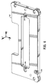
- Fig. 6 is a perspective view showing the front face of the base plate 142. This view is useful for understanding the set screw engagement regions 202, 204, 206 that form the mechanical interface between the ball points of the bracket set screws 164, 166, 168 and the base plate 142.
- set screw engagement region 204 has a conical, preferably hardened, indentation.
- set screw engagement region 202 which the ball point of the set screw 264 engages, has a depressed, V-shaped, and hardened, engagement region. This allows set screw 164 to move or slide along the y-axis relative to the base plate
Landscapes
- Engineering & Computer Science (AREA)
- Multimedia (AREA)
- Signal Processing (AREA)
- Facsimile Scanning Arrangements (AREA)
- Facsimile Heads (AREA)
- Electrophotography Configuration And Component (AREA)
Applications Claiming Priority (2)
| Application Number | Priority Date | Filing Date | Title |
|---|---|---|---|
| US09/090,041 US6473205B1 (en) | 1998-06-03 | 1998-06-03 | Image sensor module adjustable in six degrees of freedom for use with an image acquisition device |
| US90041 | 1998-06-03 |
Publications (2)
| Publication Number | Publication Date |
|---|---|
| EP0963101A2 true EP0963101A2 (de) | 1999-12-08 |
| EP0963101A3 EP0963101A3 (de) | 2001-10-31 |
Family
ID=22220972
Family Applications (1)
| Application Number | Title | Priority Date | Filing Date |
|---|---|---|---|
| EP99201701A Withdrawn EP0963101A3 (de) | 1998-06-03 | 1999-05-28 | Bildsensormodul mit sechs Freiheitsgraden für den Gebrauch zusammen mit einer Bilderfassungsvorrichtung |
Country Status (3)
| Country | Link |
|---|---|
| US (1) | US6473205B1 (de) |
| EP (1) | EP0963101A3 (de) |
| JP (1) | JP2000022907A (de) |
Cited By (2)
| Publication number | Priority date | Publication date | Assignee | Title |
|---|---|---|---|---|
| EP1585308A1 (de) * | 2004-04-02 | 2005-10-12 | Agfa-Gevaert AG | Vorrichtung zum Auslesen von in einer Phosphorschicht gespeicherten Röntgeninformation |
| CN107999330A (zh) * | 2017-12-29 | 2018-05-08 | 科睿驰(深圳)医疗科技发展有限公司 | 一种基于视觉处理的自动化导管涂覆设备和方法 |
Families Citing this family (23)
| Publication number | Priority date | Publication date | Assignee | Title |
|---|---|---|---|---|
| JP3950637B2 (ja) * | 2000-03-09 | 2007-08-01 | キヤノン株式会社 | 画像読取ユニット及び画像読取装置 |
| US6545266B2 (en) * | 2000-12-11 | 2003-04-08 | Silitek Corporation | Four-direction adjustable optical module |
| TW537560U (en) * | 2001-12-19 | 2003-06-11 | Avision Inc | Scanning module with an adjustable height |
| US6642511B1 (en) * | 2002-06-13 | 2003-11-04 | Max Data Systems, Inc. | Mounting apparatus for optical sensor having screw piles with annular fitting boards |
| US7375832B2 (en) * | 2002-09-20 | 2008-05-20 | Datamax Corporation | Adjustable sensor assembly for printers |
| TWI262363B (en) * | 2003-10-21 | 2006-09-21 | Asml Netherlands Bv | An assembly, a lithographic apparatus, and a device manufacturing method |
| US7090177B2 (en) * | 2003-11-19 | 2006-08-15 | Eastman Kodak Company | Device for optics alignment and mounting |
| TWI268103B (en) * | 2005-08-12 | 2006-12-01 | Primax Electronics Ltd | Optical module with adjustable device for adjusting an optical track |
| JP2008235983A (ja) * | 2007-03-16 | 2008-10-02 | Canon Inc | 画像読み取り装置 |
| US8269890B2 (en) | 2007-05-15 | 2012-09-18 | E-Image Data Corporation | Digital microform imaging apparatus |
| JP5043614B2 (ja) * | 2007-12-05 | 2012-10-10 | 株式会社リコー | 画像形成装置及びキャリッジ |
| US20090168116A1 (en) * | 2007-12-26 | 2009-07-02 | Chengwu Cui | Method and System For Calibrating A Scanner Having A Scan Bar Including Sensor Elements |
| US20100283885A1 (en) * | 2009-05-11 | 2010-11-11 | Shih-Schon Lin | Method for aligning pixilated micro-grid polarizer to an image sensor |
| TWI444686B (zh) * | 2011-05-31 | 2014-07-11 | Altek Corp | 對位裝置 |
| CN105651178A (zh) * | 2016-03-16 | 2016-06-08 | 苏州富强科技有限公司 | 一种基于cmos拍摄成像的测量系统 |
| CN105841630A (zh) * | 2016-03-16 | 2016-08-10 | 苏州富强科技有限公司 | 一种基于点激光飞行扫描的测量系统 |
| CN105806225A (zh) * | 2016-03-16 | 2016-07-27 | 苏州富强科技有限公司 | 一种基于线激光拍摄成像的测量系统 |
| CN105651179B (zh) * | 2016-03-16 | 2018-07-27 | 苏州富强科技有限公司 | 一种补光可调且自动装夹的视觉成像测量系统 |
| CN105651175A (zh) * | 2016-03-16 | 2016-06-08 | 苏州富强科技有限公司 | 一种基于ccd飞行拍摄成像的测量系统 |
| US11598852B2 (en) * | 2019-12-27 | 2023-03-07 | Beijing Voyager Technology Co., Ltd. | Kinematic mount for active receiver alignment with multi-degree-of-freedom |
| US11614520B2 (en) | 2019-12-27 | 2023-03-28 | Beijing Voyager Technology Co., Ltd. | Kinematic mount for active galvo mirror alignment with multi-degree-of-freedom |
| USD1018343S1 (en) * | 2020-12-08 | 2024-03-19 | Beijing Voyager Technology Co., Ltd. | Light detection and ranging (LIDAR) component |
| USD1035470S1 (en) * | 2020-12-08 | 2024-07-16 | Beijing Voyager Technology Co., Ltd. | Light detection and ranging (LIDAR) component |
Family Cites Families (6)
| Publication number | Priority date | Publication date | Assignee | Title |
|---|---|---|---|---|
| US4408231A (en) | 1981-07-31 | 1983-10-04 | International Business Machines Corporation | Method and apparatus for calibrating a linear array scanning system |
| JPH0310460A (ja) * | 1989-06-07 | 1991-01-18 | Fuji Xerox Co Ltd | 画像読取装置の位置調整方法および装置 |
| US5303064A (en) | 1991-02-20 | 1994-04-12 | Kent Johnson | Image scanner with calibration mechanism to obtain full dynamic range and compensated linear output |
| US5252818A (en) | 1991-08-22 | 1993-10-12 | Vision Ten, Inc. | Method and apparatus for improved scanner accuracy using a linear sensor array |
| US5444481A (en) | 1993-01-15 | 1995-08-22 | Sanyo Machine Works, Ltd. | Method of calibrating a CCD camera |
| US5696609A (en) * | 1995-06-29 | 1997-12-09 | Agfa Division, Bayer Corporation | Illumination system for a flat-bed scanning system |
-
1998
- 1998-06-03 US US09/090,041 patent/US6473205B1/en not_active Expired - Lifetime
-
1999
- 1999-05-10 JP JP11128623A patent/JP2000022907A/ja active Pending
- 1999-05-28 EP EP99201701A patent/EP0963101A3/de not_active Withdrawn
Cited By (3)
| Publication number | Priority date | Publication date | Assignee | Title |
|---|---|---|---|---|
| EP1585308A1 (de) * | 2004-04-02 | 2005-10-12 | Agfa-Gevaert AG | Vorrichtung zum Auslesen von in einer Phosphorschicht gespeicherten Röntgeninformation |
| US7498598B2 (en) | 2004-04-02 | 2009-03-03 | Agfa-Gevaert Healthcare Gmbh | System for reading out X-ray information stored in a phosphor layer |
| CN107999330A (zh) * | 2017-12-29 | 2018-05-08 | 科睿驰(深圳)医疗科技发展有限公司 | 一种基于视觉处理的自动化导管涂覆设备和方法 |
Also Published As
| Publication number | Publication date |
|---|---|
| US6473205B1 (en) | 2002-10-29 |
| JP2000022907A (ja) | 2000-01-21 |
| EP0963101A3 (de) | 2001-10-31 |
Similar Documents
| Publication | Publication Date | Title |
|---|---|---|
| US6473205B1 (en) | Image sensor module adjustable in six degrees of freedom for use with an image acquisition device | |
| US5883663A (en) | Multiple image camera for measuring the alignment of objects in different planes | |
| US5943089A (en) | Method and apparatus for viewing an object and for viewing a device that acts upon the object | |
| EP2091223B1 (de) | Bildlesevorrichtung und Bilderzeugungsvorrichtung | |
| US6958769B2 (en) | High resolution sheet metal scanner with independent tracking light source | |
| EP0809926B1 (de) | Bestückungsautomat für bauelemente | |
| US7433092B2 (en) | Transparency media adapter and methods of use thereof | |
| US6157467A (en) | CCD rotary-alignment device for optical scanner | |
| US8154774B2 (en) | Optical unit, image reading device, and image forming apparatus | |
| US6239885B1 (en) | Image reading apparatus and adjusting method for the same | |
| US5753908A (en) | Photoelectric imaging device photosensor array alignment apparatus and method | |
| JP2002171387A (ja) | 画像読取装置 | |
| US20020105689A1 (en) | Scanner | |
| US6097026A (en) | CCD self-alignment device for optical scanner | |
| US6073844A (en) | CCD shift-alignment device for optical scanner | |
| CN2569176Y (zh) | 焦深调整装置 | |
| JP2004126447A (ja) | 画像読取装置 | |
| JP3642692B2 (ja) | 画像読取装置 | |
| JP2000035548A (ja) | 光走査装置の固定構造 | |
| JP2818187B2 (ja) | 画像読取装置及び画像読取装置の製造方法 | |
| JP4458593B2 (ja) | 光量検出部材およびこれを備える画像読取装置 | |
| JP2000059581A (ja) | 光センサ調整装置およびその調整方法 | |
| JP2001217991A (ja) | 画像読み取り装置 | |
| CN1937693A (zh) | 图像感测单元及其组装方法,以及扫描仪和多功能打印机 | |
| EP0567179A1 (de) | Optisch aneinandergefügte elektro-optische Bauteile |
Legal Events
| Date | Code | Title | Description |
|---|---|---|---|
| PUAI | Public reference made under article 153(3) epc to a published international application that has entered the european phase |
Free format text: ORIGINAL CODE: 0009012 |
|
| AK | Designated contracting states |
Kind code of ref document: A2 Designated state(s): AT BE CH CY DE DK ES FI FR GB GR IE IT LI LU MC NL PT SE Kind code of ref document: A2 Designated state(s): DE FR GB |
|
| AX | Request for extension of the european patent |
Free format text: AL;LT;LV;MK;RO;SI |
|
| PUAL | Search report despatched |
Free format text: ORIGINAL CODE: 0009013 |
|
| AK | Designated contracting states |
Kind code of ref document: A3 Designated state(s): AT BE CH CY DE DK ES FI FR GB GR IE IT LI LU MC NL PT SE |
|
| AX | Request for extension of the european patent |
Free format text: AL;LT;LV;MK;RO;SI |
|
| 17P | Request for examination filed |
Effective date: 20020502 |
|
| AKX | Designation fees paid |
Free format text: DE FR GB |
|
| STAA | Information on the status of an ep patent application or granted ep patent |
Free format text: STATUS: THE APPLICATION HAS BEEN WITHDRAWN |
|
| 18W | Application withdrawn |
Effective date: 20040320 |