EP0963148A2 - System zur elektromagnetischen Schirmung einer Leiterplatte - Google Patents
System zur elektromagnetischen Schirmung einer Leiterplatte Download PDFInfo
- Publication number
- EP0963148A2 EP0963148A2 EP99304063A EP99304063A EP0963148A2 EP 0963148 A2 EP0963148 A2 EP 0963148A2 EP 99304063 A EP99304063 A EP 99304063A EP 99304063 A EP99304063 A EP 99304063A EP 0963148 A2 EP0963148 A2 EP 0963148A2
- Authority
- EP
- European Patent Office
- Prior art keywords
- shielding
- top surface
- replacement cover
- circuit board
- enclosure
- Prior art date
- Legal status (The legal status is an assumption and is not a legal conclusion. Google has not performed a legal analysis and makes no representation as to the accuracy of the status listed.)
- Withdrawn
Links
- 239000002184 metal Substances 0.000 claims abstract description 15
- 229910052751 metal Inorganic materials 0.000 claims abstract description 15
- 239000000853 adhesive Substances 0.000 claims abstract description 10
- 230000001070 adhesive effect Effects 0.000 claims abstract description 10
- 239000007769 metal material Substances 0.000 claims abstract description 6
- 239000011888 foil Substances 0.000 claims abstract description 5
- 238000000034 method Methods 0.000 claims description 10
- ATJFFYVFTNAWJD-UHFFFAOYSA-N Tin Chemical compound [Sn] ATJFFYVFTNAWJD-UHFFFAOYSA-N 0.000 claims description 6
- 229910000831 Steel Inorganic materials 0.000 claims description 4
- 239000010959 steel Substances 0.000 claims description 4
- 238000005476 soldering Methods 0.000 claims description 2
- 238000005452 bending Methods 0.000 claims 1
- 239000000463 material Substances 0.000 description 9
- 238000004519 manufacturing process Methods 0.000 description 4
- 229910000906 Bronze Inorganic materials 0.000 description 2
- 229910000881 Cu alloy Inorganic materials 0.000 description 2
- OAICVXFJPJFONN-UHFFFAOYSA-N Phosphorus Chemical compound [P] OAICVXFJPJFONN-UHFFFAOYSA-N 0.000 description 2
- 239000010974 bronze Substances 0.000 description 2
- KUNSUQLRTQLHQQ-UHFFFAOYSA-N copper tin Chemical compound [Cu].[Sn] KUNSUQLRTQLHQQ-UHFFFAOYSA-N 0.000 description 2
- 150000002739 metals Chemical class 0.000 description 2
- 238000012986 modification Methods 0.000 description 2
- 230000004048 modification Effects 0.000 description 2
- 238000009423 ventilation Methods 0.000 description 2
- 238000003466 welding Methods 0.000 description 2
- 239000006096 absorbing agent Substances 0.000 description 1
- 229910045601 alloy Inorganic materials 0.000 description 1
- 239000000956 alloy Substances 0.000 description 1
- DMFGNRRURHSENX-UHFFFAOYSA-N beryllium copper Chemical compound [Be].[Cu] DMFGNRRURHSENX-UHFFFAOYSA-N 0.000 description 1
- 230000015572 biosynthetic process Effects 0.000 description 1
- 230000000694 effects Effects 0.000 description 1
- 230000005684 electric field Effects 0.000 description 1
- 230000005670 electromagnetic radiation Effects 0.000 description 1
- 239000012467 final product Substances 0.000 description 1
- 238000009434 installation Methods 0.000 description 1
- 238000004806 packaging method and process Methods 0.000 description 1
- 230000035699 permeability Effects 0.000 description 1
- 230000035939 shock Effects 0.000 description 1
- 229910000679 solder Inorganic materials 0.000 description 1
- 239000010935 stainless steel Substances 0.000 description 1
- 229910001220 stainless steel Inorganic materials 0.000 description 1
- 210000003813 thumb Anatomy 0.000 description 1
Images

Classifications
-
- H—ELECTRICITY
- H05—ELECTRIC TECHNIQUES NOT OTHERWISE PROVIDED FOR
- H05K—PRINTED CIRCUITS; CASINGS OR CONSTRUCTIONAL DETAILS OF ELECTRIC APPARATUS; MANUFACTURE OF ASSEMBLAGES OF ELECTRICAL COMPONENTS
- H05K9/00—Screening of apparatus or components against electric or magnetic fields
- H05K9/0007—Casings
- H05K9/002—Casings with localised screening
- H05K9/0022—Casings with localised screening of components mounted on printed circuit boards [PCB]
- H05K9/0024—Shield cases mounted on a PCB, e.g. cans or caps or conformal shields
- H05K9/0032—Shield cases mounted on a PCB, e.g. cans or caps or conformal shields having multiple parts, e.g. frames mating with lids
-
- Y—GENERAL TAGGING OF NEW TECHNOLOGICAL DEVELOPMENTS; GENERAL TAGGING OF CROSS-SECTIONAL TECHNOLOGIES SPANNING OVER SEVERAL SECTIONS OF THE IPC; TECHNICAL SUBJECTS COVERED BY FORMER USPC CROSS-REFERENCE ART COLLECTIONS [XRACs] AND DIGESTS
- Y10—TECHNICAL SUBJECTS COVERED BY FORMER USPC
- Y10S—TECHNICAL SUBJECTS COVERED BY FORMER USPC CROSS-REFERENCE ART COLLECTIONS [XRACs] AND DIGESTS
- Y10S428/00—Stock material or miscellaneous articles
- Y10S428/901—Printed circuit
-
- Y—GENERAL TAGGING OF NEW TECHNOLOGICAL DEVELOPMENTS; GENERAL TAGGING OF CROSS-SECTIONAL TECHNOLOGIES SPANNING OVER SEVERAL SECTIONS OF THE IPC; TECHNICAL SUBJECTS COVERED BY FORMER USPC CROSS-REFERENCE ART COLLECTIONS [XRACs] AND DIGESTS
- Y10—TECHNICAL SUBJECTS COVERED BY FORMER USPC
- Y10T—TECHNICAL SUBJECTS COVERED BY FORMER US CLASSIFICATION
- Y10T156/00—Adhesive bonding and miscellaneous chemical manufacture
- Y10T156/10—Methods of surface bonding and/or assembly therefor
- Y10T156/1052—Methods of surface bonding and/or assembly therefor with cutting, punching, tearing or severing
- Y10T156/1056—Perforating lamina
-
- Y—GENERAL TAGGING OF NEW TECHNOLOGICAL DEVELOPMENTS; GENERAL TAGGING OF CROSS-SECTIONAL TECHNOLOGIES SPANNING OVER SEVERAL SECTIONS OF THE IPC; TECHNICAL SUBJECTS COVERED BY FORMER USPC CROSS-REFERENCE ART COLLECTIONS [XRACs] AND DIGESTS
- Y10—TECHNICAL SUBJECTS COVERED BY FORMER USPC
- Y10T—TECHNICAL SUBJECTS COVERED BY FORMER US CLASSIFICATION
- Y10T156/00—Adhesive bonding and miscellaneous chemical manufacture
- Y10T156/10—Methods of surface bonding and/or assembly therefor
- Y10T156/1052—Methods of surface bonding and/or assembly therefor with cutting, punching, tearing or severing
- Y10T156/1062—Prior to assembly
-
- Y—GENERAL TAGGING OF NEW TECHNOLOGICAL DEVELOPMENTS; GENERAL TAGGING OF CROSS-SECTIONAL TECHNOLOGIES SPANNING OVER SEVERAL SECTIONS OF THE IPC; TECHNICAL SUBJECTS COVERED BY FORMER USPC CROSS-REFERENCE ART COLLECTIONS [XRACs] AND DIGESTS
- Y10—TECHNICAL SUBJECTS COVERED BY FORMER USPC
- Y10T—TECHNICAL SUBJECTS COVERED BY FORMER US CLASSIFICATION
- Y10T156/00—Adhesive bonding and miscellaneous chemical manufacture
- Y10T156/10—Methods of surface bonding and/or assembly therefor
- Y10T156/1052—Methods of surface bonding and/or assembly therefor with cutting, punching, tearing or severing
- Y10T156/1062—Prior to assembly
- Y10T156/1064—Partial cutting [e.g., grooving or incising]
-
- Y—GENERAL TAGGING OF NEW TECHNOLOGICAL DEVELOPMENTS; GENERAL TAGGING OF CROSS-SECTIONAL TECHNOLOGIES SPANNING OVER SEVERAL SECTIONS OF THE IPC; TECHNICAL SUBJECTS COVERED BY FORMER USPC CROSS-REFERENCE ART COLLECTIONS [XRACs] AND DIGESTS
- Y10—TECHNICAL SUBJECTS COVERED BY FORMER USPC
- Y10T—TECHNICAL SUBJECTS COVERED BY FORMER US CLASSIFICATION
- Y10T156/00—Adhesive bonding and miscellaneous chemical manufacture
- Y10T156/10—Methods of surface bonding and/or assembly therefor
- Y10T156/1052—Methods of surface bonding and/or assembly therefor with cutting, punching, tearing or severing
- Y10T156/1082—Partial cutting bonded sandwich [e.g., grooving or incising]
-
- Y—GENERAL TAGGING OF NEW TECHNOLOGICAL DEVELOPMENTS; GENERAL TAGGING OF CROSS-SECTIONAL TECHNOLOGIES SPANNING OVER SEVERAL SECTIONS OF THE IPC; TECHNICAL SUBJECTS COVERED BY FORMER USPC CROSS-REFERENCE ART COLLECTIONS [XRACs] AND DIGESTS
- Y10—TECHNICAL SUBJECTS COVERED BY FORMER USPC
- Y10T—TECHNICAL SUBJECTS COVERED BY FORMER US CLASSIFICATION
- Y10T225/00—Severing by tearing or breaking
- Y10T225/30—Breaking or tearing apparatus
-
- Y—GENERAL TAGGING OF NEW TECHNOLOGICAL DEVELOPMENTS; GENERAL TAGGING OF CROSS-SECTIONAL TECHNOLOGIES SPANNING OVER SEVERAL SECTIONS OF THE IPC; TECHNICAL SUBJECTS COVERED BY FORMER USPC CROSS-REFERENCE ART COLLECTIONS [XRACs] AND DIGESTS
- Y10—TECHNICAL SUBJECTS COVERED BY FORMER USPC
- Y10T—TECHNICAL SUBJECTS COVERED BY FORMER US CLASSIFICATION
- Y10T428/00—Stock material or miscellaneous articles
- Y10T428/15—Sheet, web, or layer weakened to permit separation through thickness
-
- Y—GENERAL TAGGING OF NEW TECHNOLOGICAL DEVELOPMENTS; GENERAL TAGGING OF CROSS-SECTIONAL TECHNOLOGIES SPANNING OVER SEVERAL SECTIONS OF THE IPC; TECHNICAL SUBJECTS COVERED BY FORMER USPC CROSS-REFERENCE ART COLLECTIONS [XRACs] AND DIGESTS
- Y10—TECHNICAL SUBJECTS COVERED BY FORMER USPC
- Y10T—TECHNICAL SUBJECTS COVERED BY FORMER US CLASSIFICATION
- Y10T83/00—Cutting
- Y10T83/04—Processes
- Y10T83/0495—Making and using a registration cut
Definitions
- the present invention relates generally to a shielding system for a printed circuit board, and in particular, to a shielding system having an integral shielding enclosure with a fixed cover that may be permanently removed, and a replacement cover for attaching thereto.
- a conventional metal shield cover or can, is mounted to a printed circuit board by using fasteners appropriate for the purpose. Thereafter, the metal shield is soldered or welded to selected grounding strips on the printed circuit board at selected locations of its side walls. Using solder or welding to mechanically hold and electrically connect the metal shield to the printed circuit board permanently affixes the metal shield over the selected electronic component(s).
- the printed circuit board After assembling the completed printed circuit board, including the required metal shields, the printed circuit board will generally be subjected to a "burn-in" stage during which it is subjected to elevated temperature tests. If one of the electronic components should fail during the burn-in, however, that component must be replaced. Thus, it becomes necessary to desolder or unweld the metal shield from the printed circuit board in order to obtain access to the failed component and replace the same. This is very difficult to successfully accomplish and, more than likely, the entire printed circuit board will be destroyed.
- shielding devices such as that disclosed in U.S. Patent No. 4,754,101 of the present assignee, the entire contents of which are hereby incorporated by reference, have included a separate wall enclosure and a removable cover.
- the cover is resiliently held in place by deflectable engagement prongs extending from an upper edge of the wall enclosure.
- the presence of the resiliently held cover allows access to the underlying electronic component, should the same be required, however, the manufacturing costs associated with the formation of the engagement prongs are also increased.
- an electromagnetic shielding system including a shielding enclosure having a plurality of side walls and an integral top surface.
- the top surface includes a scored line for allowing removal of an interior portion of the top surface to thereby define a remaining perimeter rim.
- a replacement cover is also included for attachment to the remaining cover rim after the interior portion is removed.
- the replacement cover may include a metal foil having an adhesive surface or a metal sheet material.
- the present invention further provides a method for shielding and obtaining access to a component on a printed circuit board.
- the method includes providing a printed circuit board having a component encompassed by a shielding enclosure.
- the shielding enclosure includes a plurality of side walls and an integral top surface having a scored line which defines an interior portion.
- the scored line on the top surface of the shielding enclosure is severed and the interior portion of the top surface defined by the scored line is removed to thereby leave a remaining perimeter rim on the printed circuit board and allow access to the component within the rim.
- the scored line may be severed by grasping a hole in the top surface of the shielding enclosure and applying force.
- a replacement cover is also provided for the top surface of the shielding enclosure. The replacement cover is attached to the shielding enclosure to thereby encompass and shield the component.
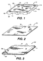
- an electromagnetic shielding system for a printed circuit board in accordance with the present invention is shown generally by reference numeral 10.
- Shielding system 10 is designed to be welded, soldered, or otherwise fixed to a printed circuit board (not shown) during the manufacture thereof and thereby encompass and shield one or more underlying electronic components that are mounted on the printed circuit board.
- the electromagnetic shielding system 10 can be used to shield either a section or component of a printed circuit board or the entire board.
- Shielding system 10 includes an enclosure 12 defined by side walls 14 and a top surface 16 integrally joined therewith.
- the walls 14 could be formed into any reasonable configuration.
- the walls 14 are formed into a square, rectangle or other quadrilateral shape.
- the walls 14 and the top surface 16 are preferably made from a metallic material, such as tin plated steel.
- tin plated phosphor bronze, beryllium copper and other alloys of copper may of course also be used depending upon the required shielding.
- the material be metals that are capable of being readily soldered or welded and capable of low resistance electrical conductivity.
- the primary purpose of the shield is to reduce magnetic field interference, it is generally preferable to use a steel or other alloy which has a relatively high permeability at low frequencies.
- the material may be plated with a low resistance metal, such as tin.
- a copper alloy as will be readily apparent to one skilled in the art of electromagnetic shielding.
- the walls 14 and the top surface 16 preferably have a thickness of approximately 0.005 in.
- the metal material is tin plated steel, tin plated phosphor bronze, or stainless steel.
- Other thicknesses could of course also be used depending upon the material used to form the walls 14 and the top surface 16 and the end use environment in which the enclosure 12 will be placed.
- Each of the walls 14 includes a side member portion 18 and, preferably, one or more projections 20 extending from a lower edge of the side member portion 18.
- the projections 20 are preferably soldered to the printed circuit board to obtain a surface mount thereon, although through hole mounting or any other type of known mounting arrangement could also be utilized.
- the enclosures 12 of the present invention are adaptable for tape and reel packaging for use in standard automated pick and place equipment or, alternatively, the enclosures of the present invention may be packed in trays for correct orientation within an automated syste m or, still further, they be may packed in bulk as may be required by conventional equipment.
- the top surface 16 includes a scored line 22 extending parallel to the perimeter thereof. Although illustrated as being scored substantially continuously around the perimeter, it is also within the scope of the present invention that the scored line 22 may not be continuous and that it may include portions therealong that are not scored, such as along one or more sides of the top surface for example. A non-continuous scored line 22 may be used in order to increase the rigidity of the top surface 16 and its ability to withstand vibrations and shocks encountered during use.
- the scored line 22 is preferably spaced approximately 0.020 in. from the outer perimeter edge in the illustrated embodiment, however, it will be apparent to one skilled in the art that other placements could of course also be used depending upon the specific configuration and size of the enclosure and the top surface thereof.
- the scored line 22 allows an interior portion 26 of the top surface 16 to be removed, and thereby define a remaining perimeter rim 28, as shown in FIG. 4. Being able to remove an integral portion of the top surface, i.e., the interior portion 26, allows access to be gained to an underlying electronic component without removing the entire enclosure 12, as discussed in further detail below.
- the top surface 16 may include air vents 24 in the form of small circular holes as shown in FIG. 1.
- the vents 24 illustrated in the corners of the top surface assist, in conjunction with the score line 22, in allowing for the break away of the interior portion.
- the vents or holes 24 disposed in the interior portion 26 can additionally serve as thumb nail grips for starting the removal of the same.
- the top surface 16 may include, instead of or in addition to the vents 24, louvers or perforations for ventilation, heat sink components, handles, or other hardware to suit a specific need or function.
- material to absorb electrical energy such as a microwave absorber, may be attached or bonded to the inside of the top surface 16.
- a replacement cover 30 is shown in accordance with the present invention.
- the replacement cover 30 is preferably made from the same metal material as the enclosure 12, although a different metal material could of course also be used.
- the replacement cover 30 also includes vents 24 and a plurality of etched formed or lanced elements 32 which are provided in order to assist in self locating the cover 30 on top of the perimeter rim.
- Replacement cover 30 is attached to the perimeter rim 28 of the enclosure 12 by welding, soldering, or any other conventional attachment means.
- Replacement cover 30' includes a main portion 38 generally corresponding in shape to the configuration of the perimeter rim 28.
- cover 30' also includes a plurality of side flanges 40 extending therefrom and a plurality of predefined bend lines 42 disposed between the main portion 38 and the flanges 40.
- Replacement cover 30' is made from a metal foil and includes an adhesive surface 34 that is, at least initially, provided with a release paper 36.
- Replacement cover 30' is attached to the perimeter rim 28 of the enclosure, and also preferably the side walls 14, by removing the release paper 36 to expose the adhesive surface 34, and by bringing the adhesive surface 34 into contact with the rim 28 and folding down the side flanges 40 along the bend lines 42 to thereby bring the flanges 40 into contact with the side walls 14, as shown in FIG. 5.
- shielding system 10 of the present invention can be described as follows.
- shielding enclosure 12 is disposed over one or more electric or electronic components or the entire board, in order to reduce the electromagnetic interference with adjacent components.
- the score line 22 allows the interior portion 26 of the enclosure 12 to be removed using the vents 24 as g rips or otherwise exerting a slight force to sever the score line 22 and completely separate the interior portion 26.
- the perimeter rim 28 of the enclosure 12 will remain attached to the printed circuit board (not shown).
- the shielding system 10 of the present invention allows access to the failed component such that the component itself may be replaced, rather than declaring the entire printed circuit board an entire loss.
- the replacement cover 30, 30' is then attached to the perimeter rim 28 in order to again form a complete shielding enclosure over the electronic component. As shown in FIG. 5, the replacement cover 30' is attached to the perimeter 28 by applying the adhesive surface 34 directly thereto. Similarly, replacement cover 30 is welded, soldered, or otherwise mechanically attached to the perimeter 28. In each instance, the replacement cover 30, 30' together with the perimeter rim 28 encompass and shield the one or more underlying electronic components that are mounted on the printed circuit board.
- the shielding system 10 of the present invention may be easily and inexpensively manufactured, in comparison with the resiliently held covers of the prior art.
- the enclosure 12 including the cover 16 is stamped or punched from a sheet material.
- the score line 22 and air vents 24 are also cut into the sheet material at this stage.
- the sides of the enclosure are bent to form the side member portions 18 and thereby obtain the final product.
- the covers 30, 30' are likewise easily formed using standard sheet metal or sheet foil processing techniques.
Landscapes
- Engineering & Computer Science (AREA)
- Microelectronics & Electronic Packaging (AREA)
- Shielding Devices Or Components To Electric Or Magnetic Fields (AREA)
Applications Claiming Priority (3)
| Application Number | Priority Date | Filing Date | Title |
|---|---|---|---|
| US89238 | 1998-06-02 | ||
| US09/089,238 US6136131A (en) | 1998-06-02 | 1998-06-02 | Method of shielding and obtaining access to a component on a printed circuit board |
| US89238P | 1998-06-15 |
Publications (2)
| Publication Number | Publication Date |
|---|---|
| EP0963148A2 true EP0963148A2 (de) | 1999-12-08 |
| EP0963148A3 EP0963148A3 (de) | 2000-04-05 |
Family
ID=22216499
Family Applications (1)
| Application Number | Title | Priority Date | Filing Date |
|---|---|---|---|
| EP99304063A Withdrawn EP0963148A3 (de) | 1998-06-02 | 1999-05-26 | System zur elektromagnetischen Schirmung einer Leiterplatte |
Country Status (5)
| Country | Link |
|---|---|
| US (2) | US6136131A (de) |
| EP (1) | EP0963148A3 (de) |
| JP (1) | JPH11354967A (de) |
| CA (1) | CA2273468A1 (de) |
| SG (1) | SG74731A1 (de) |
Cited By (5)
| Publication number | Priority date | Publication date | Assignee | Title |
|---|---|---|---|---|
| WO2001076342A1 (en) * | 2000-04-03 | 2001-10-11 | Matsushita Electric Industrial Co., Ltd. | Portable radio apparatus |
| FR2819979A1 (fr) * | 2001-01-19 | 2002-07-26 | Mitsubishi Electric Corp | Structure de blindage pour des elements de circuits electroniques |
| US7005573B2 (en) | 2003-02-13 | 2006-02-28 | Parker-Hannifin Corporation | Composite EMI shield |
| US7326862B2 (en) | 2003-02-13 | 2008-02-05 | Parker-Hannifin Corporation | Combination metal and plastic EMI shield |
| FR2961346A1 (fr) * | 2010-06-15 | 2011-12-16 | Peugeot Citroen Automobiles Sa | Composant electronique avec protection contre les decharges electrostatiques et procede de protection d'un tel composant electronique |
Families Citing this family (83)
| Publication number | Priority date | Publication date | Assignee | Title |
|---|---|---|---|---|
| US6136131A (en) * | 1998-06-02 | 2000-10-24 | Instrument Specialties Company, Inc. | Method of shielding and obtaining access to a component on a printed circuit board |
| US20070137653A1 (en) * | 2000-03-13 | 2007-06-21 | Wood Thomas J | Ventilation interface for sleep apnea therapy |
| JP2001244127A (ja) * | 2000-02-29 | 2001-09-07 | Murata Mfg Co Ltd | 高周波部品および通信装置 |
| JP2002094689A (ja) * | 2000-06-07 | 2002-03-29 | Sony Computer Entertainment Inc | プログラム実行システム、プログラム実行装置、中継装置、および記録媒体 |
| US20020084300A1 (en) * | 2000-12-29 | 2002-07-04 | Charles Elkins | Apparatus and method for separating circuit boards |
| US6377475B1 (en) | 2001-02-26 | 2002-04-23 | Gore Enterprise Holdings, Inc. | Removable electromagnetic interference shield |
| US6649827B2 (en) | 2001-09-28 | 2003-11-18 | Siemens Information & Communication Moblie, Llc | Radio frequency shield enclosure for a printed circuit board |
| US6949706B2 (en) | 2001-09-28 | 2005-09-27 | Siemens Information And Communication Mobile, Llc | Radio frequency shield for electronic equipment |
| US6870090B2 (en) * | 2001-11-01 | 2005-03-22 | International Business Machines Corporation | System for protecting against leakage of sensitive information from compromising electromagnetic emissions from computing systems |
| DE60110267T2 (de) * | 2001-12-17 | 2005-09-22 | Nokia Corporation | Abschirmelement für elektrische und/oder elektronische komponenten einer elektrischen oder elektronischen schaltung |
| DE60327962D1 (de) * | 2002-04-03 | 2009-07-30 | Panasonic Corp | Eingebautes Halbleitermodul im Millimeterwellenband |
| US6744640B2 (en) | 2002-04-10 | 2004-06-01 | Gore Enterprise Holdings, Inc. | Board-level EMI shield with enhanced thermal dissipation |
| US6683795B1 (en) * | 2002-04-10 | 2004-01-27 | Amkor Technology, Inc. | Shield cap and semiconductor package including shield cap |
| US6897371B1 (en) | 2002-08-27 | 2005-05-24 | A K Stamping Co. Inc. | One-piece shielding enclosure with selective interior access, and method and blank therefor |
| US7868723B2 (en) * | 2003-02-26 | 2011-01-11 | Analogic Corporation | Power coupling device |
| US8350655B2 (en) * | 2003-02-26 | 2013-01-08 | Analogic Corporation | Shielded power coupling device |
| US9490063B2 (en) | 2003-02-26 | 2016-11-08 | Analogic Corporation | Shielded power coupling device |
| US9368272B2 (en) | 2003-02-26 | 2016-06-14 | Analogic Corporation | Shielded power coupling device |
| US6831224B2 (en) * | 2003-04-25 | 2004-12-14 | Nokia Corporation | One-piece manufactured shielding casing for accommodating electronic functional elements |
| US7672699B2 (en) * | 2003-06-19 | 2010-03-02 | Samsung Electronics Co., Ltd. | Driving apparatus using magnetic substance for sliding type portable wireless terminal |
| GB2404089B (en) * | 2003-07-11 | 2007-05-02 | Craig Rochford | Printed circuit board assembly |
| US7084356B2 (en) * | 2003-12-08 | 2006-08-01 | Laird Technologies, Inc. | Replacement cover for electromagnetic shielding system |
| TWI351918B (en) | 2004-01-29 | 2011-11-01 | Laird Technologies Inc | Ultra-low height electromagnetic interference shie |
| US7218095B2 (en) * | 2004-07-30 | 2007-05-15 | Verigy (Singapore) Pte. Ltd. | Method and apparatus for electromagnetic interference shielding in an automated test system |
| US7087835B2 (en) * | 2004-10-19 | 2006-08-08 | Bi-Link Metal Specialties Inc. | Apparatus and method for shielding printed circuit boards |
| US7629674B1 (en) * | 2004-11-17 | 2009-12-08 | Amkor Technology, Inc. | Shielded package having shield fence |
| USD522517S1 (en) | 2005-02-25 | 2006-06-06 | Laird Technologies, Inc. | Push-fit EMI shield |
| JP2006310965A (ja) * | 2005-04-26 | 2006-11-09 | Orion Denki Kk | デジタル放送受信装置 |
| US7491899B2 (en) * | 2005-10-06 | 2009-02-17 | Laird Technologies, Inc. | EMI shields and related manufacturing methods |
| TW200730494A (en) * | 2005-10-10 | 2007-08-16 | Glaxo Group Ltd | Novel compounds |
| WO2007057951A1 (ja) * | 2005-11-16 | 2007-05-24 | Mitsubishi Denki Kabushiki Kaisha | シールド構造 |
| US20070139904A1 (en) * | 2005-12-16 | 2007-06-21 | English Gerald R | Low-profile assemblies for providing board level EMI shielding for electrical components on opposite sides of printed circuit boards |
| USD549706S1 (en) | 2005-12-16 | 2007-08-28 | Laird Technologies, Inc. | Frame for an EMI shield assembly |
| USD549231S1 (en) | 2005-12-16 | 2007-08-21 | Laird Technologies, Inc. | Cover for an EMI shield assembly |
| TWM293660U (en) * | 2005-12-16 | 2006-07-01 | Jin-Fu Hung | Shielding structure against electromagnetic Interference |
| USD548738S1 (en) | 2005-12-16 | 2007-08-14 | Laird Technologies, Inc. | EMI shield assembly |
| US7518880B1 (en) | 2006-02-08 | 2009-04-14 | Bi-Link | Shielding arrangement for electronic device |
| US7342303B1 (en) | 2006-02-28 | 2008-03-11 | Amkor Technology, Inc. | Semiconductor device having RF shielding and method therefor |
| SE529319C2 (sv) * | 2006-03-13 | 2007-07-03 | Amc Centurion Ab | Antennanordning och bärbar radiokommunikationsanordning för en sådan antennanordning |
| US20070275237A1 (en) * | 2006-05-24 | 2007-11-29 | Syh-Tau Yeh | Electromagnetic shielding tape |
| US7724542B2 (en) * | 2006-12-30 | 2010-05-25 | Intel Corporation | Reworkable RF shield |
| US7488902B2 (en) * | 2007-01-25 | 2009-02-10 | Laird Technologies, Inc. | Electromagnetic interference shielding apparatus and methods of making the same |
| JP4047366B1 (ja) * | 2007-01-30 | 2008-02-13 | 東レエンジニアリング株式会社 | 超音波トランスデューサ |
| US20080233426A1 (en) * | 2007-03-21 | 2008-09-25 | Gaviglia John J | Steel sheeting for use in room size radio frequency shielded enclosures and method for making improved steel sheeting |
| JP2008288523A (ja) * | 2007-05-21 | 2008-11-27 | Fujitsu Media Device Kk | 電子部品,及びその製造方法 |
| US7898066B1 (en) | 2007-05-25 | 2011-03-01 | Amkor Technology, Inc. | Semiconductor device having EMI shielding and method therefor |
| US7903431B2 (en) * | 2007-06-14 | 2011-03-08 | Laird Technologies, Inc. | Electromagnetic interference shielding apparatus |
| US7745910B1 (en) | 2007-07-10 | 2010-06-29 | Amkor Technology, Inc. | Semiconductor device having RF shielding and method therefor |
| US7504592B1 (en) | 2007-08-31 | 2009-03-17 | Laird Technologies, Inc. | Electromagnetic interference shields and related manufacturing methods |
| US8031485B2 (en) * | 2007-09-07 | 2011-10-04 | Autosplice, Inc. | Electronic shielding apparatus and methods |
| CN201142457Y (zh) * | 2007-12-29 | 2008-10-29 | 富士康(昆山)电脑接插件有限公司 | 电连接器组件 |
| US8008753B1 (en) | 2008-04-22 | 2011-08-30 | Amkor Technology, Inc. | System and method to reduce shorting of radio frequency (RF) shielding |
| US8265329B2 (en) * | 2008-09-05 | 2012-09-11 | Apple Inc. | Compact housing for portable electronic device with internal speaker |
| US8126170B2 (en) | 2008-09-05 | 2012-02-28 | Apple Inc. | Electromagnetic interference shields with piezos |
| US7965495B2 (en) * | 2008-10-13 | 2011-06-21 | Apple Inc. | Battery connector structures for electronic devices |
| CN101730459B (zh) * | 2008-10-17 | 2013-02-20 | 深圳富泰宏精密工业有限公司 | 屏蔽罩及其制作方法 |
| US7915715B2 (en) * | 2008-11-25 | 2011-03-29 | Amkor Technology, Inc. | System and method to provide RF shielding for a MEMS microphone package |
| US8129824B1 (en) | 2008-12-03 | 2012-03-06 | Amkor Technology, Inc. | Shielding for a semiconductor package |
| US8102032B1 (en) | 2008-12-09 | 2012-01-24 | Amkor Technology, Inc. | System and method for compartmental shielding of stacked packages |
| US8012868B1 (en) | 2008-12-15 | 2011-09-06 | Amkor Technology Inc | Semiconductor device having EMI shielding and method therefor |
| US7851894B1 (en) | 2008-12-23 | 2010-12-14 | Amkor Technology, Inc. | System and method for shielding of package on package (PoP) assemblies |
| US7960818B1 (en) | 2009-03-04 | 2011-06-14 | Amkor Technology, Inc. | Conformal shield on punch QFN semiconductor package |
| US20100246143A1 (en) * | 2009-03-26 | 2010-09-30 | Richard Hung Minh Dinh | Electromagnetic Interference Shielding for Compact Electronic Devices |
| US20100257732A1 (en) * | 2009-04-14 | 2010-10-14 | Ziberna Frank J | Shielding Arrangement for Electronic Device |
| US8093691B1 (en) | 2009-07-14 | 2012-01-10 | Amkor Technology, Inc. | System and method for RF shielding of a semiconductor package |
| US8362598B2 (en) * | 2009-08-26 | 2013-01-29 | Amkor Technology Inc | Semiconductor device with electromagnetic interference shielding |
| CN201967298U (zh) * | 2010-02-04 | 2011-09-07 | 卓英社有限公司 | 用于emi屏蔽的屏蔽设备及包括该屏蔽设备的pcb |
| US8199518B1 (en) | 2010-02-18 | 2012-06-12 | Amkor Technology, Inc. | Top feature package and method |
| US8946886B1 (en) | 2010-05-13 | 2015-02-03 | Amkor Technology, Inc. | Shielded electronic component package and method |
| US8508023B1 (en) | 2010-06-17 | 2013-08-13 | Amkor Technology, Inc. | System and method for lowering contact resistance of the radio frequency (RF) shield to ground |
| US8383960B2 (en) * | 2010-07-14 | 2013-02-26 | A.K. Stamping Company, Inc. | One-piece board level shielding with peel-away feature |
| CN102378562A (zh) * | 2010-08-19 | 2012-03-14 | 深圳富泰宏精密工业有限公司 | 电磁屏蔽罩及印刷电路板装置 |
| KR101129621B1 (ko) * | 2011-07-04 | 2012-03-28 | 김선기 | 전자파 차폐 케이스용 금속 스트립 어셈블리, 이를 적용한 차폐 케이스 및 그 제조방법 |
| US20140139985A1 (en) * | 2012-11-12 | 2014-05-22 | Industrial Technology Research Institute | Environmental sensitive electronic device package |
| US9538693B2 (en) * | 2013-03-15 | 2017-01-03 | A.K. Stamping Company, Inc. | Aluminum EMI / RF shield |
| DE102015001148B4 (de) * | 2015-01-30 | 2019-04-11 | e.solutions GmbH | Anordnung und Verfahren zur elektromagnetischen Abschirmung |
| KR102382008B1 (ko) | 2015-07-30 | 2022-04-04 | 삼성전자주식회사 | 쉴드 커버 및 그것을 포함하는 전자 장치 |
| KR102452781B1 (ko) | 2015-12-15 | 2022-10-12 | 삼성전자주식회사 | 차폐 구조를 포함하는 전자 장치 |
| WO2017122220A1 (en) * | 2016-01-11 | 2017-07-20 | Ranga Reddy Seelam | Mobile phone casing |
| US10542644B2 (en) | 2016-12-14 | 2020-01-21 | A.K. Stamping Company, Inc. | Two-piece solderable shield |
| US10177095B2 (en) | 2017-03-24 | 2019-01-08 | Amkor Technology, Inc. | Semiconductor device and method of manufacturing thereof |
| US10497650B2 (en) | 2017-04-13 | 2019-12-03 | Amkor Technology, Inc. | Semiconductor device and manufacturing method thereof |
| US10881036B2 (en) * | 2019-03-04 | 2020-12-29 | Cisco Technology, Inc. | Minimizing or alleviating stress in a surface of a sheet metal structure caused by addition of surface features to the structure |
Family Cites Families (25)
| Publication number | Priority date | Publication date | Assignee | Title |
|---|---|---|---|---|
| US3809233A (en) * | 1971-02-03 | 1974-05-07 | Western Electric Co | Method of and package for transporting articles |
| US4754101A (en) * | 1986-10-23 | 1988-06-28 | Instrument Specialties Co., Inc. | Electromagnetic shield for printed circuit board |
| FI85794C (fi) * | 1989-07-05 | 1992-05-25 | Nokia Mobira Oy | Foerfarande foer att skydda ett kretskort eller en del daerav mot stoerningar som alstrats av elektromagnetisk interferens, och skyddshoelje foer anvaendning i foerfarandet. |
| DE4008335A1 (de) * | 1990-03-15 | 1991-09-26 | Panavia Aircraft Gmbh | Abgeschirmter pc |
| US5676812A (en) * | 1990-03-24 | 1997-10-14 | Canon Kabushiki Kaisha | Electronic equipment with an adhesive member to intercept electromagnetic waves |
| FI91931C (fi) * | 1991-10-22 | 1994-08-25 | Nokia Mobile Phones Ltd | EMC-kotelo |
| MY108723A (en) * | 1992-08-28 | 1996-11-30 | Thomson Consumer Electronics Inc | Printed circuit board shield assembly for a tuner and the like |
| US5354951A (en) * | 1993-03-15 | 1994-10-11 | Leader Tech, Inc. | Circuit board component shielding enclosure and assembly |
| US5436802A (en) * | 1994-03-16 | 1995-07-25 | Motorola | Method and apparatus for shielding an electrical circuit that is disposed on a substrate |
| JPH0818265A (ja) * | 1994-06-29 | 1996-01-19 | Molex Inc | プリント回路基板上での電磁波等のシ−ルド方法 及びその為のシ−ルドカバ− |
| US5495399A (en) * | 1994-07-05 | 1996-02-27 | Motorola, Inc. | Shield with detachable grasp support member |
| AU7979394A (en) * | 1994-08-19 | 1996-03-14 | W.L. Gore & Associates, Inc. | A see-through radiation shielded assembly |
| US5586011A (en) * | 1994-08-29 | 1996-12-17 | At&T Global Information Solutions Company | Side plated electromagnetic interference shield strip for a printed circuit board |
| DE19509553C1 (de) * | 1995-03-16 | 1996-07-18 | Bosch Gmbh Robert | Abschirmhaube |
| US5614694A (en) * | 1995-03-31 | 1997-03-25 | Motorola, Inc. | One piece open and closable metal RF shield |
| US5635775A (en) * | 1995-04-14 | 1997-06-03 | Colburn; Richard H. | Printed circuit board mount electro-magnetic interference suppressor |
| US5594200A (en) * | 1995-06-09 | 1997-01-14 | Ramsey Electronics, Inc. | Electromagnetic isolation chamber |
| US5633786A (en) * | 1995-08-21 | 1997-05-27 | Motorola | Shield assembly and method of shielding suitable for use in a communication device |
| DE19732618A1 (de) * | 1996-07-31 | 1998-02-05 | Motorola Inc | Abschirmung für eine elektrische Schaltung auf einem Substrat |
| DE19636182A1 (de) * | 1996-09-06 | 1998-03-12 | Philips Patentverwaltung | Abschirmgehäuse für elektronische Bauelemente |
| JPH10145078A (ja) | 1996-11-06 | 1998-05-29 | Sony Corp | 電子機器筐体の不要輻射電磁波の遮蔽構造 |
| US5917708A (en) * | 1997-03-24 | 1999-06-29 | Qualcomm Incorporated | EMI shield apparatus for printed wiring board |
| US6169666B1 (en) * | 1997-05-29 | 2001-01-02 | U.S. Philips Corporation | Electromagnetic shielding screen and circuit support having such a screen |
| US6136131A (en) * | 1998-06-02 | 2000-10-24 | Instrument Specialties Company, Inc. | Method of shielding and obtaining access to a component on a printed circuit board |
| US6178097B1 (en) * | 1999-01-22 | 2001-01-23 | Dial Tool Industries, Inc. | RF shield having removable cover |
-
1998
- 1998-06-02 US US09/089,238 patent/US6136131A/en not_active Expired - Lifetime
-
1999
- 1999-05-26 EP EP99304063A patent/EP0963148A3/de not_active Withdrawn
- 1999-05-28 SG SG1999002734A patent/SG74731A1/en unknown
- 1999-06-01 JP JP11154159A patent/JPH11354967A/ja not_active Revoked
- 1999-06-01 CA CA002273468A patent/CA2273468A1/en not_active Abandoned
-
2000
- 2000-05-02 US US09/563,950 patent/US6501016B1/en not_active Expired - Lifetime
Cited By (8)
| Publication number | Priority date | Publication date | Assignee | Title |
|---|---|---|---|---|
| WO2001076342A1 (en) * | 2000-04-03 | 2001-10-11 | Matsushita Electric Industrial Co., Ltd. | Portable radio apparatus |
| US7113740B2 (en) | 2000-04-03 | 2006-09-26 | Matsushita Electric Industrial Co., Ltd. | Portable radio apparatus |
| EP1740034A1 (de) * | 2000-04-03 | 2007-01-03 | Matsushita Electric Industrial Co., Ltd. | Tragbares Funkgerät |
| FR2819979A1 (fr) * | 2001-01-19 | 2002-07-26 | Mitsubishi Electric Corp | Structure de blindage pour des elements de circuits electroniques |
| US6593523B2 (en) | 2001-01-19 | 2003-07-15 | Mitsubishi Denki Kabushiki Kaisha | Shield structure for electronic circuit parts |
| US7005573B2 (en) | 2003-02-13 | 2006-02-28 | Parker-Hannifin Corporation | Composite EMI shield |
| US7326862B2 (en) | 2003-02-13 | 2008-02-05 | Parker-Hannifin Corporation | Combination metal and plastic EMI shield |
| FR2961346A1 (fr) * | 2010-06-15 | 2011-12-16 | Peugeot Citroen Automobiles Sa | Composant electronique avec protection contre les decharges electrostatiques et procede de protection d'un tel composant electronique |
Also Published As
| Publication number | Publication date |
|---|---|
| US6501016B1 (en) | 2002-12-31 |
| SG74731A1 (en) | 2000-08-22 |
| EP0963148A3 (de) | 2000-04-05 |
| JPH11354967A (ja) | 1999-12-24 |
| CA2273468A1 (en) | 1999-12-02 |
| US6136131A (en) | 2000-10-24 |
Similar Documents
| Publication | Publication Date | Title |
|---|---|---|
| US6136131A (en) | Method of shielding and obtaining access to a component on a printed circuit board | |
| US7663895B2 (en) | Electromagnetic shielding device for printed circuit board | |
| EP2031950B1 (de) | Elektromagnetische Abschirmungen und zugehöriges Herstellungsverfahren | |
| US6178097B1 (en) | RF shield having removable cover | |
| EP1130953B1 (de) | Elektromagnetisch geschirmte schicht, elektromagnetisch geschirmte struktur und unterhaltungsgerät | |
| US6870091B2 (en) | Two-piece electrical RF shield and method of manufacturing the same | |
| CA2084499C (en) | Emi shield apparatus and methods | |
| US6903262B2 (en) | Shielding element for electric and/or electronic components of an electric and/or electronic circuit | |
| US20130120957A1 (en) | Rf shielding for electronic components | |
| EP0381378A2 (de) | Verfahren zur Herstellung des Chassis eines Funktelefons und nach diesem Verfahren hergestelltes Chassis | |
| US5748449A (en) | Electrical enclosure for radio | |
| GB2297868A (en) | EMI/RFI shielding device | |
| US8455771B2 (en) | Electromagnetic shielding device | |
| US7609530B2 (en) | Conductive elastomeric shielding device and method of forming same | |
| US8063727B2 (en) | Conductive shielding device | |
| EP0702512B1 (de) | Abschirmungsvorrichtung und Verfahren zur Montage | |
| JP2009117773A (ja) | 電子機器 | |
| JP2000196280A (ja) | 電磁気周波数妨害シ―ルド用の面着式クリップ | |
| JPH11330771A (ja) | 低構造の無線周波数シ―ルド | |
| US20050237727A1 (en) | Radio frequency shield covers | |
| CN1242687A (zh) | 印刷电路板的电磁屏蔽装置 | |
| US6950309B2 (en) | Power amplifier module assembly | |
| HK1025462A (en) | Electromagnetic shielding system for printed circuit board | |
| JP3566237B2 (ja) | シールドボックス構造及び、固定部品、シールドボックス | |
| GB2315923A (en) | Shield for an electrical circuit on a substrate |
Legal Events
| Date | Code | Title | Description |
|---|---|---|---|
| PUAI | Public reference made under article 153(3) epc to a published international application that has entered the european phase |
Free format text: ORIGINAL CODE: 0009012 |
|
| AK | Designated contracting states |
Kind code of ref document: A2 Designated state(s): AT BE CH CY DE DK ES FI FR GB GR IE IT LI LU MC NL PT SE |
|
| AX | Request for extension of the european patent |
Free format text: AL;LT;LV;MK;RO;SI |
|
| PUAL | Search report despatched |
Free format text: ORIGINAL CODE: 0009013 |
|
| AK | Designated contracting states |
Kind code of ref document: A3 Designated state(s): AT BE CH CY DE DK ES FI FR GB GR IE IT LI LU MC NL PT SE |
|
| AX | Request for extension of the european patent |
Free format text: AL;LT;LV;MK;RO;SI |
|
| 17P | Request for examination filed |
Effective date: 20000901 |
|
| AKX | Designation fees paid |
Free format text: AT BE CH CY DE DK ES FI FR GB GR IE IT LI LU MC NL PT SE |
|
| STAA | Information on the status of an ep patent application or granted ep patent |
Free format text: STATUS: THE APPLICATION IS DEEMED TO BE WITHDRAWN |
|
| 18D | Application deemed to be withdrawn |
Effective date: 20011203 |