EP0964425A2 - Appareil pour le traitment d'une cible par un faisceau d'ions uniformement neu tralisé - Google Patents
Appareil pour le traitment d'une cible par un faisceau d'ions uniformement neu tralisé Download PDFInfo
- Publication number
- EP0964425A2 EP0964425A2 EP99110048A EP99110048A EP0964425A2 EP 0964425 A2 EP0964425 A2 EP 0964425A2 EP 99110048 A EP99110048 A EP 99110048A EP 99110048 A EP99110048 A EP 99110048A EP 0964425 A2 EP0964425 A2 EP 0964425A2
- Authority
- EP
- European Patent Office
- Prior art keywords
- ion beam
- processing apparatus
- electrode
- microwave
- wave guide
- Prior art date
- Legal status (The legal status is an assumption and is not a legal conclusion. Google has not performed a legal analysis and makes no representation as to the accuracy of the status listed.)
- Withdrawn
Links
Images


Classifications
-
- H—ELECTRICITY
- H01—ELECTRIC ELEMENTS
- H01J—ELECTRIC DISCHARGE TUBES OR DISCHARGE LAMPS
- H01J37/00—Discharge tubes with provision for introducing objects or material to be exposed to the discharge, e.g. for the purpose of examination or processing thereof
- H01J37/02—Details
- H01J37/04—Arrangements of electrodes and associated parts for generating or controlling the discharge, e.g. electron-optical arrangement or ion-optical arrangement
- H01J37/08—Ion sources; Ion guns
-
- H—ELECTRICITY
- H01—ELECTRIC ELEMENTS
- H01J—ELECTRIC DISCHARGE TUBES OR DISCHARGE LAMPS
- H01J27/00—Ion beam tubes
- H01J27/02—Ion sources; Ion guns
- H01J27/16—Ion sources; Ion guns using high-frequency excitation, e.g. microwave excitation
- H01J27/18—Ion sources; Ion guns using high-frequency excitation, e.g. microwave excitation with an applied axial magnetic field
-
- H—ELECTRICITY
- H01—ELECTRIC ELEMENTS
- H01J—ELECTRIC DISCHARGE TUBES OR DISCHARGE LAMPS
- H01J2237/00—Discharge tubes exposing object to beam, e.g. for analysis treatment, etching, imaging
- H01J2237/004—Charge control of objects or beams
- H01J2237/0041—Neutralising arrangements
-
- H—ELECTRICITY
- H01—ELECTRIC ELEMENTS
- H01J—ELECTRIC DISCHARGE TUBES OR DISCHARGE LAMPS
- H01J2237/00—Discharge tubes exposing object to beam, e.g. for analysis treatment, etching, imaging
- H01J2237/06—Sources
- H01J2237/08—Ion sources
- H01J2237/0815—Methods of ionisation
- H01J2237/0817—Microwaves
-
- H—ELECTRICITY
- H01—ELECTRIC ELEMENTS
- H01J—ELECTRIC DISCHARGE TUBES OR DISCHARGE LAMPS
- H01J2237/00—Discharge tubes exposing object to beam, e.g. for analysis treatment, etching, imaging
- H01J2237/30—Electron or ion beam tubes for processing objects
- H01J2237/31—Processing objects on a macro-scale
- H01J2237/3142—Ion plating
Definitions
- the present invention is related to an ion beam processing apparatus, and in particular, to an ion beam processing apparatus which is suitable for processing a work piece by etching with a large current and a large diameter ion beam.
- an etching apparatus for etching a work piece using an ion beam as disclosed in JPA Laid-Open No. 63-157887.
- an ion beam neutralizing method is employed, wherein a plasma is generated by a microwave discharge in a neutralizing unit disposed near to the ion beam, and electrons are supplied from the plasma through a small opening to the ion beam so as to neutralize the ion beam.
- This method assures a longer time of operation compared to an ion beam neutralizing method which uses a hollow cathode containing a filament for emitting thermoelectrons, and thus is suitable for neutralizing a reactive ion beam. Further, because no filament such as tungsten is used, contamination of the work piece by heavy metals constituting the filament can be prevented, thereby providing for a clean ion beam processing.
- the conventional neutralizing method has a limitation in providing for a large current and large diameter ion beam because of the following reasons to be described below.
- annular electrode 8 is disposed between a plasma generating chamber 1 and a processing chamber 23 and the processing chamber 23 is connected to the plasma generating chamber 1 through the annular electrode 8.
- the annular electrode 8 forms a portion of the vacuum chamber providing the vacuum of the vacuum chamber, and needs to be constructed with a thick metal to be strong in order to prevent the vacuum chamber from an atmospheric pressure.
- the thick metal of the annular electrode 8 make the annular magnetic field generated by the many permanent magnets 9, difficult sufficiently to be formed inside of the vacuum chamber through the thick metal.
- the present invention is provided referring to this problem.
- An ion beam processing apparatus in the present invention comprises an ion source for producing a processing plasma, a processing chamber provided as a vacuum chamber for accommodating a process target being disposed adjacent to said ion source, an extract electrode for extracting an ion beam from said processing plasma into the processing chamber so as to irradiate on said process target, an annular electrode disposed in said processing chamber for forming an annular magnetic field therein, through which said ion beam being irradiated on said process, and a wave guide for introducing microwave through an opening provided on a wall forming said processing chamber, into said annular magnetic field.
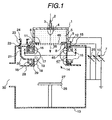
- FIG 1 is a schematic cross-sectional view of an ion beam processing apparatus according to a first embodiment of the invention.
- Figure 2 is a schematic cross-sectional view of a main part of a guide wave indicative of its structure for introducing the microwave according to the invention.
- the ion beam processing apparatus of Figs. 1 and 2 is comprised of ion source 1, acceleration electrode 6, deceleration electrode 9, protection electrode (third electrode) 11, microwave neutralizer 14, and processing chamber 13.
- the processing chamber 13, which constitutes a vacuum container is disposed in juxtaposition with the ion source 1, and is connected thereto via insulation spacer 12.
- the microwave neutralizer 14 a part of which that does not constitute the vacuum container, is disposed outside the processing chamber 13, and a main part thereof is disposed inside the processing chamber 13.
- the ion source 1 which is composed as a container for generating a processing plasma has a plasma gas inlet pipe 3 connected at its upper side, a plasma generation filament 4 disposed therein, and an opening portion 46 formed at its bottom side.
- Plasma gas 2 which is introduced into the ion source 1 through gas inlet tube 3 is heated by conduction of filament 4 so as to obtain a sufficient energy to become a plasma 5.
- Acceleration electrode 6 is disposed in the opening portion 46 of the ion source 1 and firmly connected thereto. This acceleration electrode 6 is connected to an acceleration power supply 7 via ion source 1. Both the acceleration electrode 6 and ion source 1 are applied a positive voltage from the acceleration power supply 7.
- a deceleration electrode 9 is mounted on the acceleration electrode 6 via an electrode insulation spacer 8.
- the deceleration electrode 9 is supplied with a negative voltage from a deceleration power supply 10.
- the acceleration electrode 6 and the deceleration electrode 9 are disposed in juxtaposition with the ion source 1, and are composed as an extraction electrode for extracting a processing ion beam 36 from plasma 5 within the ion source 1 into processing chamber 13 and irradiating the same on a wafer (process target) 27 placed on a holder 26.
- Protection electrode (third electrode) 11 is mounted on the deceleration electrode 9 via insulation spacer 8, and the protection electrode 11 is further connected to microwave neutralizer 14 via conductor 45.
- Microwave neutralizer 14 is connected to neutralizing power supply 25.
- a potential of the protection electrode 11 and microwave neutralizer 14 is maintained at a negative potential relative to a potential of the processing chamber 13. Namely, by setting the potential of the protection electrode 11 at a negative potential relative to the potential of processing chamber 13, the ions in the neutralizing plasma generated by the microwave neutralizer 14 are collected by protection electrode 11 before they collide on the deceleration electrode 9, thereby preventing for the deceleration electrode 9 to be damaged by ion bombardment.
- the microwave neutralizer 14 of the invention which functions as the neutralizing plasma generation means and the ion collection means, is comprised of external (atmospheric side) wave guide 24, quartz plate 23, internal (vacuum side) wave guide 21, a plurality of permanent magnets 16, annular electrode 47, and deposition prevention plate 28, and wherein the annular electrode 47 is disposed inside the processing chamber 13 aligned with the center line of ion source 1 and is firmly fixed thereto via insulation spacer 15.
- the external (atmospheric side) wave guide 24 disposed outside the processing chamber 13 and with interposition of quartz plate (microwave transparent plate) 23 which hermetically seals the opening 22 formed in the processing chamber 13 for introducing the microwave thereinto is firmly fixed on an outer wall of processing chamber 13 as an external portion of the wave guide for guiding microwave 34 generated in a microwave generator (not shown) to the opening 22.
- a recess portion 31 and O-ring groove 32 are formed on the outer surface of processing chamber 13 and in the vicinity of the opening 22.
- O-ring 33 is mounted in the O-ring groove 32, and quartz plate 23 is disposed on the O-ring 33.
- the quartz plate 23 is coupled to the opening 22 as supported by an end portion of the wave-guide 24.
- the end portion of the wave guide 24 is firmly fixed to the outer wall of processing chamber 13 by means of fixtures such as insulated screws, insulated bolts and the like (not shown). Namely, by connecting firmly the wave guide 24 outside the opening 22 of processing chamber 13 via O-ring 33 and quartz plate 23, vacuum in processing chamber 13 is maintained.
- Internal wave guide (on vacuum side) 21 provided for guiding the microwave passing through quartz plate 23 is firmly fixed at its one end to an inner wall of processing chamber 13 via insulation spacer 15, and at the other end thereof coupled to annular electrode 47 formed into a straight tube integral therewith. Further, the wave guide 21 is provided with a deflection portion 20 for reflecting microwave 34 passing through quartz plate 23 toward a direction of annular electrode 47 on its way so as to prevent for high energy conducting particles from depositing on quartz plate 23 which serves as the microwave introduction window.
- Annular electrode 47 which is formed approximately into a cylindrical shape as an annular member which surrounds a periphery of a propagation region of processing ion beam 36, is provided with an opening 19 for introducing microwave 34 into a region inside the annular member 47. Further, the annular electrode 47, likewise the protection electrode 11, is connected to neutralizing power supply 27, and the annular electrode 47 is applied with a voltage which is negative relative to that of the processing chamber 13. A pair of permanent magnets 16 having their magnetic poles counterposed is disposed in plural numbers at a predetermined space along an external periphery of annular electrode 47.
- arrays of plural permanent magnets (magnetic substances) 16 which constitute the magnetic field forming members of the invention are arranged with their magnetic polarities counterposed along the outer periphery of the annular electrode 47.
- Each pair of permanent magnets 16 disposed in opposite polarities produces a line of magnetic force 17, and a magnetic field 18 is allowed to be formed, on the internal side of annular electrode 47, having a flux density of electron cyclotron resonance corresponding to a frequency of microwave 34.
- Magnetic field 18 is allowed to form a multi ring cusp magnetic field as will be described later.
- annular electrode 47 is connected to a deposition prevention plate 28 via insulation spacer 29.
- This deposition prevention plate 28 is provided for preventing a sputter from wafer 27 placed on holder 26 from depositing on microwave neutralizer 14. This deposition prevention plate 28 is maintained at the same potential as that of the processing chamber 13 (which is normally at the earth potential). Further, an exhaust opening 30 is formed in the processing chamber 13 so as to allow for the inside of the processing chamber 13 to be vacuum deaerated as required by an exhaust system connected to the opening 30.
- an exhaust opening 30 is formed in the processing chamber 13 so as to allow for the inside of the processing chamber 13 to be vacuum deaerated as required by an exhaust system connected to the opening 30.
- microwave 34 of 2.45 GHz is introduced from the microwave generator into the atmospheric side wave guide 24, microwave 34 guided through wave guide 24 is allowed to pass through quartz plate 23 to enter vacuum side wave guide 21.
- this microwave 34 is reflected on the deflector 20 and is introduced into the inner region of annular electrode 47 through opening 19, this microwave 34 is absorbed by electrons by resonance absorption in the magnetic field 18 with an electron cyclotron resonance flux density of 875 gauss, thereby generating high energy electrons.
- This high energy electrons move along the line of magnetic force 17 reciprocating in the multi ring cusp magnetic field formed between the juxtaposed magnets and on the inner surface of annular electrode 47.
- the high energy electrons revolve in a circumferential direction by a magnetic field grading drift action as indicated in Fig. 4 along annular (band) electrode 47 so as to ionize the gas and generate a neutralizing plasma in an uniform ring shape.
- a portion of the neutralizing plasma having a good containment of the plasma is represented as a high-density plasma portion 35.
- This plasma portion 35 is in contact with the annular electrode 47 and the ion beam 36.
- microwave 34 introduced from the wave guide 21 is deflected outwardly in the directions of electron cyclotron resonance magnetic fields 18 so as to facilitate its arrival thereto, thereby ensuring an efficient absorption of microwave 34.
- each opening connected to each of a plurality of vacuum side wave guides 21 allows for a plurality of microwaves 34 to be introduced therein through the plurality of vacuum side wave guides 21, thereby capable of neutralizing a larger current, broader diameter ion beam 36.
- one end of wave-guide 21 can be formed into a tapered opening type wave-guide 41, which can be connected integral with annular electrode 41.
- the wave guide 21 having tapered opening type wave guide 41 at its one end is provided, because its microwave is caused to propagate in wider radial directions, it becomes possible to irradiate microwave 34 more efficiently into electron cyclotron resonance magnetic field 18, ensuring for microwave 34 to reach the electron cyclotron resonance magnetic field 18 more easily.
- wave guide 21 allowing for an insertion fit-in connection method can be provided wherein one end of wave guide 21 is formed into a tapered opening type wave guide 41, which can be inserted into the opening 19 for connection therebetween.
- FIG. 8 A schematic block diagram indicating a second embodiment of the invention is shown in Fig. 8.
- a feature of the second embodiment of the invention different from the preceding embodiment resides in that although the negative voltage is applied to annular electrode 47 by connecting the same to neutralizing power supply 25 in the preceding embodiment, its negative voltage is applied from neutralizing power supply 25 to a band electrode 43 which is fixed via electrode insulation spacer 42 on the internal side of annular electrode 47, and through opening 48 formed in annular electrode 47 for internal connection therebetween.
- Other elements for construction thereof are the same as those in the preceding embodiment of the invention of Fig. 1.
- the band electrode 43 provided as a second annular electrode is formed into a cylindrical shape, and allows microwave 34 to be introduced through opening 49. The same is further connected to protection electrode 11 via conductor 45.
- wave guide 21 can be formed integral with annular electrode 47, otherwise as indicated in Fig. 9(a) the one end of wave guide 21 can be formed into tapered opening type wave guide 41 having spacer 44 mounted on its end, which can be inserted into opening 19.
- one end of wave guide 21 can be formed into a straight tube opening type wave guide 40 having spacer 44 mounted to this end, which can be inserted into opening 19 for connection therebetween.
Landscapes
- Chemical & Material Sciences (AREA)
- Engineering & Computer Science (AREA)
- Combustion & Propulsion (AREA)
- Analytical Chemistry (AREA)
- Drying Of Semiconductors (AREA)
- Electron Sources, Ion Sources (AREA)
- Plasma Technology (AREA)
- Welding Or Cutting Using Electron Beams (AREA)
- ing And Chemical Polishing (AREA)
Applications Claiming Priority (2)
| Application Number | Priority Date | Filing Date | Title |
|---|---|---|---|
| JP16027198 | 1998-06-09 | ||
| JP16027198A JP3364830B2 (ja) | 1998-06-09 | 1998-06-09 | イオンビーム加工装置 |
Publications (2)
| Publication Number | Publication Date |
|---|---|
| EP0964425A2 true EP0964425A2 (fr) | 1999-12-15 |
| EP0964425A3 EP0964425A3 (fr) | 2004-02-11 |
Family
ID=15711400
Family Applications (1)
| Application Number | Title | Priority Date | Filing Date |
|---|---|---|---|
| EP99110048A Withdrawn EP0964425A3 (fr) | 1998-06-09 | 1999-05-21 | Apparaeil pour le traitement d'une cible par un faisceau d'ions uniformement neutralisé |
Country Status (3)
| Country | Link |
|---|---|
| US (2) | US6184625B1 (fr) |
| EP (1) | EP0964425A3 (fr) |
| JP (1) | JP3364830B2 (fr) |
Cited By (1)
| Publication number | Priority date | Publication date | Assignee | Title |
|---|---|---|---|---|
| DE10024883A1 (de) * | 2000-05-19 | 2001-11-29 | Bosch Gmbh Robert | Plasmaätzanlage |
Families Citing this family (20)
| Publication number | Priority date | Publication date | Assignee | Title |
|---|---|---|---|---|
| US8314064B2 (en) * | 1998-07-31 | 2012-11-20 | Massachusetts Institute Of Technology | Uridine administration stimulates membrane production |
| KR100382720B1 (ko) * | 2000-08-30 | 2003-05-09 | 삼성전자주식회사 | 반도체 식각 장치 및 이를 이용한 반도체 소자의 식각 방법 |
| US6922019B2 (en) * | 2001-05-17 | 2005-07-26 | The Regents Of The University Of California | Microwave ion source |
| JP3641716B2 (ja) * | 2001-05-23 | 2005-04-27 | 株式会社日立製作所 | イオンビーム加工装置およびその方法 |
| US6541921B1 (en) * | 2001-10-17 | 2003-04-01 | Sierra Design Group | Illumination intensity control in electroluminescent display |
| US6887341B2 (en) * | 2001-11-13 | 2005-05-03 | Tokyo Electron Limited | Plasma processing apparatus for spatial control of dissociation and ionization |
| JP3840108B2 (ja) * | 2001-12-27 | 2006-11-01 | 株式会社 Sen−Shi・アクセリス カンパニー | イオンビーム処理方法及び処理装置 |
| US7013834B2 (en) * | 2002-04-19 | 2006-03-21 | Nordson Corporation | Plasma treatment system |
| US7176469B2 (en) * | 2002-05-22 | 2007-02-13 | The Regents Of The University Of California | Negative ion source with external RF antenna |
| US6975072B2 (en) * | 2002-05-22 | 2005-12-13 | The Regents Of The University Of California | Ion source with external RF antenna |
| JP3723783B2 (ja) * | 2002-06-06 | 2005-12-07 | 東京エレクトロン株式会社 | プラズマ処理装置 |
| US7863582B2 (en) * | 2008-01-25 | 2011-01-04 | Valery Godyak | Ion-beam source |
| JP5908001B2 (ja) * | 2014-01-16 | 2016-04-26 | 東京エレクトロン株式会社 | 基板処理装置 |
| KR101816861B1 (ko) * | 2016-10-21 | 2018-01-10 | (주)제이하라 | 플라즈마 표면 처리장치 |
| JP6570144B2 (ja) | 2017-11-24 | 2019-09-04 | 国立研究開発法人宇宙航空研究開発機構 | マイクロ波プラズマ源 |
| US12159768B2 (en) * | 2019-03-25 | 2024-12-03 | Recarbon, Inc. | Controlling exhaust gas pressure of a plasma reactor for plasma stability |
| CN112343780B (zh) * | 2019-08-09 | 2021-08-13 | 哈尔滨工业大学 | 微波同轴谐振会切场推力器 |
| CN112345861B (zh) * | 2020-11-05 | 2024-11-01 | 郑州轻工业大学 | 环形磁电回旋器、实验装置及环形磁电回旋器工作方法 |
| CN113202707B (zh) * | 2021-05-12 | 2022-08-02 | 兰州空间技术物理研究所 | 一种可变直径离子推力器磁极 |
| JP7705787B2 (ja) * | 2021-11-26 | 2025-07-10 | 東京エレクトロン株式会社 | プラズマ処理装置及びプラズマ処理方法 |
Family Cites Families (6)
| Publication number | Priority date | Publication date | Assignee | Title |
|---|---|---|---|---|
| US4507588A (en) * | 1983-02-28 | 1985-03-26 | Board Of Trustees Operating Michigan State University | Ion generating apparatus and method for the use thereof |
| JPH0689465B2 (ja) | 1986-12-22 | 1994-11-09 | 株式会社日立製作所 | エツチング装置 |
| US5032202A (en) * | 1989-10-03 | 1991-07-16 | Martin Marietta Energy Systems, Inc. | Plasma generating apparatus for large area plasma processing |
| KR910016054A (ko) * | 1990-02-23 | 1991-09-30 | 미다 가쓰시게 | 마이크로 전자 장치용 표면 처리 장치 및 그 방법 |
| JPH05326452A (ja) * | 1991-06-10 | 1993-12-10 | Kawasaki Steel Corp | プラズマ処理装置及び方法 |
| JP3123735B2 (ja) | 1995-04-28 | 2001-01-15 | 株式会社日立製作所 | イオンビーム処理装置 |
-
1998
- 1998-06-09 JP JP16027198A patent/JP3364830B2/ja not_active Expired - Fee Related
-
1999
- 1999-05-21 EP EP99110048A patent/EP0964425A3/fr not_active Withdrawn
- 1999-06-08 US US09/327,502 patent/US6184625B1/en not_active Expired - Fee Related
-
2001
- 2001-01-02 US US09/750,665 patent/US6320321B2/en not_active Expired - Fee Related
Cited By (1)
| Publication number | Priority date | Publication date | Assignee | Title |
|---|---|---|---|---|
| DE10024883A1 (de) * | 2000-05-19 | 2001-11-29 | Bosch Gmbh Robert | Plasmaätzanlage |
Also Published As
| Publication number | Publication date |
|---|---|
| US20010005119A1 (en) | 2001-06-28 |
| EP0964425A3 (fr) | 2004-02-11 |
| JP3364830B2 (ja) | 2003-01-08 |
| US6320321B2 (en) | 2001-11-20 |
| JPH11354508A (ja) | 1999-12-24 |
| US6184625B1 (en) | 2001-02-06 |
Similar Documents
| Publication | Publication Date | Title |
|---|---|---|
| US6184625B1 (en) | Ion beam processing apparatus for processing work piece with ion beam being neutralized uniformly | |
| US4447732A (en) | Ion source | |
| US6803590B2 (en) | Ion beam mass separation filter, mass separation method thereof and ion source using the same | |
| KR890004880B1 (ko) | 스퍼터링 방법 및 장치 | |
| US7176469B2 (en) | Negative ion source with external RF antenna | |
| KR910010099B1 (ko) | Ecr 이온 소스 | |
| EP0283519A1 (fr) | Generateur ionique, installation de formation de films minces utilisant ce generateur et source d'ions | |
| KR100388594B1 (ko) | 이온빔처리장치 | |
| KR950012581A (ko) | 플라즈마로부터 이온 추출을 사용하는 물리적 기상 증착 | |
| JPH0360139B2 (fr) | ||
| US6246059B1 (en) | Ion-beam source with virtual anode | |
| US4737688A (en) | Wide area source of multiply ionized atomic or molecular species | |
| US5899666A (en) | Ion drag vacuum pump | |
| EP0094473B1 (fr) | Appareil et méthode pour produire un faiseau d'ions | |
| JP5850829B2 (ja) | プラズマビーム発生方法並びにプラズマ源 | |
| JP2000012293A (ja) | 中性ビーム発生装置 | |
| JPS6386864A (ja) | イオン源 | |
| JP2008128887A (ja) | プラズマ源,それを用いた高周波イオン源,負イオン源,イオンビーム処理装置,核融合用中性粒子ビーム入射装置 | |
| JPH0692638B2 (ja) | 薄膜装置 | |
| JPH06310297A (ja) | 低エネルギー中性粒子線発生方法及び装置 | |
| CA2249157C (fr) | Implantation d'ions monoenergetiques de distribution uniforme | |
| JPH0353402Y2 (fr) | ||
| JPH10275566A (ja) | イオン源 | |
| JPH0665200B2 (ja) | 高速原子線源装置 | |
| EP0095879B1 (fr) | Equipement et méthode pour le traitement des surfaces avec un faisceau d'ions à basse énergie et haute intensité |
Legal Events
| Date | Code | Title | Description |
|---|---|---|---|
| PUAI | Public reference made under article 153(3) epc to a published international application that has entered the european phase |
Free format text: ORIGINAL CODE: 0009012 |
|
| AK | Designated contracting states |
Kind code of ref document: A2 Designated state(s): AT BE CH CY DE DK ES FI FR GB GR IE IT LI LU MC NL PT SE |
|
| AX | Request for extension of the european patent |
Free format text: AL;LT;LV;MK;RO;SI |
|
| PUAL | Search report despatched |
Free format text: ORIGINAL CODE: 0009013 |
|
| AK | Designated contracting states |
Kind code of ref document: A3 Designated state(s): AT BE CH CY DE DK ES FI FR GB GR IE IT LI LU MC NL PT SE |
|
| AX | Request for extension of the european patent |
Extension state: AL LT LV MK RO SI |
|
| RIC1 | Information provided on ipc code assigned before grant |
Ipc: 7H 01J 37/08 B Ipc: 7H 01J 27/18 A |
|
| AKX | Designation fees paid | ||
| REG | Reference to a national code |
Ref country code: DE Ref legal event code: 8566 |
|
| STAA | Information on the status of an ep patent application or granted ep patent |
Free format text: STATUS: THE APPLICATION IS DEEMED TO BE WITHDRAWN |
|
| 18D | Application deemed to be withdrawn |
Effective date: 20040812 |