EP0964471B1 - Nichtstrahlender dielektrischer Wellenleiterresonator, nichtstrahlendes dielektrisches Wellenleiterfilter und damit ausgerüstete Duplexer und Sender-Empfänger - Google Patents
Nichtstrahlender dielektrischer Wellenleiterresonator, nichtstrahlendes dielektrisches Wellenleiterfilter und damit ausgerüstete Duplexer und Sender-Empfänger Download PDFInfo
- Publication number
- EP0964471B1 EP0964471B1 EP99111374A EP99111374A EP0964471B1 EP 0964471 B1 EP0964471 B1 EP 0964471B1 EP 99111374 A EP99111374 A EP 99111374A EP 99111374 A EP99111374 A EP 99111374A EP 0964471 B1 EP0964471 B1 EP 0964471B1
- Authority
- EP
- European Patent Office
- Prior art keywords
- dielectric
- groove
- dielectric strip
- nonradiative
- dielectric waveguide
- Prior art date
- Legal status (The legal status is an assumption and is not a legal conclusion. Google has not performed a legal analysis and makes no representation as to the accuracy of the status listed.)
- Expired - Lifetime
Links
- 239000004020 conductor Substances 0.000 claims description 119
- 230000005540 biological transmission Effects 0.000 claims description 9
- 239000003989 dielectric material Substances 0.000 claims description 4
- 230000008054 signal transmission Effects 0.000 claims description 2
- 238000004519 manufacturing process Methods 0.000 description 8
- 230000008878 coupling Effects 0.000 description 7
- 238000010168 coupling process Methods 0.000 description 7
- 238000005859 coupling reaction Methods 0.000 description 7
- 230000000903 blocking effect Effects 0.000 description 5
- 229910052782 aluminium Inorganic materials 0.000 description 4
- XAGFODPZIPBFFR-UHFFFAOYSA-N aluminium Chemical compound [Al] XAGFODPZIPBFFR-UHFFFAOYSA-N 0.000 description 4
- 239000000463 material Substances 0.000 description 4
- 230000015572 biosynthetic process Effects 0.000 description 3
- 229910052751 metal Inorganic materials 0.000 description 3
- 239000002184 metal Substances 0.000 description 3
- 238000000034 method Methods 0.000 description 2
- -1 polytetrafluoroethylene Polymers 0.000 description 2
- 229920001343 polytetrafluoroethylene Polymers 0.000 description 2
- 239000004810 polytetrafluoroethylene Substances 0.000 description 2
- 239000011347 resin Substances 0.000 description 2
- 229920005989 resin Polymers 0.000 description 2
- 150000002739 metals Chemical class 0.000 description 1
- 230000035939 shock Effects 0.000 description 1
Images




Classifications
-
- H—ELECTRICITY
- H01—ELECTRIC ELEMENTS
- H01P—WAVEGUIDES; RESONATORS, LINES, OR OTHER DEVICES OF THE WAVEGUIDE TYPE
- H01P1/00—Auxiliary devices
- H01P1/20—Frequency-selective devices, e.g. filters
- H01P1/2002—Dielectric waveguide filters
Definitions
- the present invention relates to a nonradiative dielectric waveguide resonator, a nonradiative dielectric waveguide filter, a duplexer and a transceiver incorporating the same, used in a motor-vehicle-mounted radar in the millimeter wave band and the microwave band, wireless LAN, or the like.
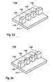
- Fig. 23 is a perspective view of a conventional nonradiative dielectric waveguide filter, in which the upper conductor plate is omitted for convenience sake.
- the filter 110a is composed of parallel upper and lower conductor plates 111 made of aluminum, etc., and a dielectric strip 112 made of polytetrafluoroethylene, etc., which is disposed between the upper and lower conductor plates 111.
- the dielectric strip 112 is composed of resonator parts 115 and input-output connection unit parts 116, which are arranged apart from each other.
- the resonator parts 115 of the dielectric strip 112 and the upper and lower conductor plates 111 form a nonradiative dielectric waveguide resonator, whereas the input-output connection unit parts 116 of the dielectric strip 112 and the upper and lower conductor plates 111 form input-output connection units.
- the distance between the upper and lower conductor plates 111 is set to no more than a half wavelength of the frequency used. This permits a position in which the dielectric strip 112 is present to be a signal-transmitting region and permits a position in which the dielectric strip 112 is not present to be a cut-off region.
- signals transmitting through the input-output connection unit couple to the nonradiative dielectric waveguide resonator through the distance between the input-output connection unit parts 116 and the resonator parts 115 of the dielectric strip 112 so as to resonate with a resonance frequency determined, for example, by the length of the signal-transmitting direction of the dielectric strip 112.
- signals are output, in which the nonradiative dielectric waveguide filter 110a acts as a band pass filter.
- the nonradiative dielectric waveguide filter 110b employed in a second conventional embodiment is also composed of the upper and lower conductor plates 111 and the dielectric strip 112 disposed between the upper and lower conductor plates 111.
- the resonator parts 115 and the input-output connection unit parts 116 of the dielectric strip 112 are connected by a dielectric strip having a narrower width.
- the nonradiative dielectric waveguide filter 110b shown in Fig. 24 also acts as a band pass filter, as in the case of the first conventional embodiment.
- a comparable filter is disclosed in T.
- the length of the signal-transmitting direction of a resonator part of a dielectric strip determines a resonance frequency
- the distance between resonator parts determines a coefficient of coupling
- the distance between an input-output connection unit part and the resonator part determines an external Q.
- the resonator part and the input-output connection unit part of the dielectric strip are arranged apart from each other. As a result, fine adjustment between their arranged positions is necessary to obtain required characteristics. Furthermore, even after the formation of the nonradiative dielectric waveguide filter, for example, shocks from the outside cause changes in their arranged positions so that filter characteristics are also changed.
- the resonator part and the input-output connection unit part of the dielectric strip are connected, their arranged positions are not likely to change.
- the present invention has been made to solve them. It is an object of the present invention to provide a nonradiative dielectric waveguide resonator and a nonradiative dielectric waveguide filter which permit easy manufacturing and have stable characteristics, and a duplexer and a transceiver which incorporate the same. This object is achieved by a resonator according to claim 1.
- a nonradiative dielectric waveguide resonator including two planar conductors disposed substantially parallel to each other with a dielectric strip disposed therebetween, having substantially the same shape of sections, which are perpendicular to a signal-transmitting direction, at least one resonance region and cut-off regions on both sides of the dielectric strip of the resonance region in the signal-transmitting direction.
- This arrangement enables use of the dielectric strip having substantially the same shape of sections, which are perpendicular to a signal-transmission direction, so that a nonradiative dielectric waveguide resonator which permits easy manufacturing and has stable characteristics can be obtained.
- the dielectric strip of the nonradiative dielectric waveguide resonator is formed of a dielectric material having uniform dielectric constant.
- a main signal-transmitting mode is preferably the LSM mode; a first groove having a bottom and conductor walls may be disposed in a position in which the conductors are opposing; the resonance region may be formed by fitting the dielectric strip into the first groove; and the cut-off regions may be formed either by fitting the dielectric strip into a second groove having lower conductor walls than those of the first groove or by disposing the dielectric strip between the conductors having no grooves.
- the first groove of the nonradiative dielectric waveguide resonator may include a bottom and conductor walls of a specified height or higher.
- a main signal-transmitting mode may be the LSE mode; a first groove having a bottom and conductor walls may be disposed in a position in which the conductors are opposing; the cut-off regions may be formed by fitting the dielectric strip into the first groove; and the resonance region may be formed either by fitting the dielectric strip into a second groove having lower conductor walls than those of the first groove or by disposing the dielectric strip between the conductors having no grooves.
- a nonradiative dielectric waveguide filter including two planar conductors disposed substantially parallel to each other, a dielectric strip having substantially the same shape of sections, which are perpendicular to a signal-transmitting direction, in which input-output connection units formed by disposing the dielectric strip between the conductors are coupled to the nonradiative dielectric waveguide resonator described above.
- a nonradiative dielectric waveguide resonator including two planar conductors disposed substantially parallel to each other and a dielectric strip having substantially the same shape of sections perpendicular to a signal-transmitting direction, the dielectric strip being disposed between the conductors, may have a resonance region and cut-off regions;
- the input-output connection units may couple to the nonradiative dielectric waveguide resonator, in which a main signal-transmitting mode may be the LSM mode;
- a first groove comprising a bottom and conductor walls may be disposed in a position in which the conductors are opposing;
- the resonance region and the input-output connection means may be formed by fitting the dielectric strip into the first groove; and the cut-off regions may be formed either by fitting the dielectric strip into a second groove having lower conductor walls than those of the first groove or by disposing the dielectric strip between the conductors having no grooves.
- a nonradiative dielectric waveguide resonator including two planar conductors disposed substantially parallel to each other and a dielectric strip having substantially the same shape of sections, which are perpendicular to a signal-transmitting direction, the dielectric strip being disposed between the conductors, may have a resonance region and cut-off regions; the input-output connection units may couple to the nonradiative dielectric waveguide resonator, in which the main signal-transmitting mode may be the LSE mode; a first groove having a bottom and conductor walls may be disposed in a position in which the conductors are opposing; the cut-off regions may be formed by fitting the dielectric strip into the first groove; and the resonance region and the input-output connection units may be formed either by fitting the dielectric strip into a second groove having lower conductor walls than those of the first groove or disposing the dielectric strip between the conductors having no grooves.
- a duplexer including at least two filters, input-output connection units connected to the filters, and an antenna connection unit connected to the filters for common use, in which at least one of the filters is the nonradiative dielectric waveguide filter described above.
- a transceiver including the duplexer; a transmission circuit connected to at least one of the input-output connection units of the duplexer; a reception circuit connected to at least one of the input-output connection units, which is different from the input-output connection unit connected to the transmission circuit; and an antenna connected to the antenna connection unit of the duplexer.
- FIG. 1 is a perspective view of the nonradiative dielectric waveguide filter of the present invention.
- the upper conductor plate thereof is omitted for convenience sake.
- a nonradiative dielectric waveguide filter 10 of the embodiment comprises parallel upper and lower conductor plates 11 made of, for example, metal-coated resin or aluminum, and a pillar dielectric strip 12 disposed between the upper and lower conductor plates 11.
- the sections of the dielectric strip 12, which are perpendicular to a signal-transmitting direction have the same rectangular shapes.
- FIG. 2 shows a sectional view along the line X-X of the perspective view shown in Fig. 1
- Fig. 3 shows a sectional view along the line Y-Y of the same view.
- the side part of the dielectric strip 12 which is fitted into the groove 20 comprising a bottom 21 and conductor walls 22 is partially covered by the conductor walls 22.
- the side of the dielectric strip 12 is not covered by the conductor.
- the LSM mode is used as a transmission mode. Additionally, setting of frequency, etc., allows the parts where the sides of the dielectric strip 12 are covered by the conductor walls 22 to be signal-transmitting regions, whereas it allows the parts where the sides are not covered by the conductor walls 22 to be cut-off regions 17. Moreover, the signal-transmitting regions serve as resonators 15 and input-output connection means 16, so that the nonradiative dielectric waveguide filter 10 serves as a band pass filter having two resonators.
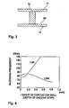
- Fig. 4 shows the relationship between the depth of a groove disposed in the conductor plate, namely, the height of the conductor wall and blocking frequencies.
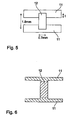
- the height of the conductor wall is represented by t in the sectional view of the nonradiative dielectric waveguide shown in Fig. 5.
- the solid line in Fig. 4 shows the relationship between the heights of the conductor wall and blocking frequencies in the case of using the LSM mode, whereas the broken line shows the same relationship in the case of using the LSE mode.
- the side parts of the dielectric strip which are partially covered by the conductor walls of the groove, serve as resonators and input-output connection means, whereas the side parts of the dielectric strip, which are not covered by the conductor walls serve as cut-off regions, when lateral grooves are further disposed in the conductor plate.
- disposing of the groove 20 in the conductor plate 11 to fit the dielectric strip 12 thereinto yields an arrangement in which the side parts of the dielectric strip 12 partially covered by the conductor walls 22 serve as resonators 15 and input-output connection means 16, whereas the side parts of the dielectric strip 12 not covered by the conductor walls 22 serves as cut-off regions 17.
- making a difference in the depth of the groove which is represented by t of the sectional view in Fig. 5, enables formation of resonators, input-output connection means, and cut-off regions.
- the region is allowed to serve as a cut-off region as long as the distance is not greater than a half wavelength of the used frequency.
- the height of the conductor wall is the lowest-level mode, and only the LSM mode as a single mode can be used by selecting frequencies, so that designing such as disposing of a bent part or the like can be easily performed.
- Fig. 1 shows an example in which the lateral grooves 25 are formed all over the horizontal direction
- the length of the signal-transmitting direction of the resonator 15 of the dielectric strip 12 mainly determines a resonance frequency; the distance between the resonators 15 determines the coupling coefficient; and the distance between the input-output connection means 16 and the resonator 15 determines the external Q.
- the depths of the groove 20 and the lateral grooves 25 formed in the conductor plate 11 influence a resonance frequency, a coupling coefficient, and an external Q.
- a resonance frequency, a coupling coefficient, and an external Q can be adjusted by cutting away a part of the dielectric strip 12, or by adding a material having a dielectric constant different from that of the dielectric strip 12 to the dielectric strip 12. Since these are methods conducted by cutting or adding a small amount of material, the condition does not substantially change in which the shapes of sections perpendicular to the signal-transmitting direction of the dielectric strip 12 are approximately the same.
- the present invention provides a nonradiative dielectric waveguide filter in which characteristic changes are small with respect to temperature changes. That is, metals such as aluminum generally used for a conductor plate have a smaller linear expansion coefficient than polytetrafluoroethylene used for a dielectric strip.
- the configuration of the dielectric strip changes more; thereby a significant level of change occurs in the resonance frequency and the like.
- the configuration of the conductor plate of the lateral groove, etc. defines a resonator and a cut-off region. Accordingly, influence due to temperature changes can be small, and changes in the characteristics of the nonradiative dielectric waveguide filter are also reduced.
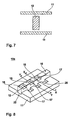
- Fig. 9 is a perspective view of a nonradiative dielectric waveguide filter 10b according to a second embodiment
- Fig. 10 is a sectional view along the line Z-Z of the view shown in Fig. 9
- Fig. 11 is a sectional view along the line W-W of the view shown in Fig. 9.
- nonradiative dielectric waveguide filter 10b of this embodiment as shown in Fig. 9, two dielectric strips 12 having a brim 13 are bonded together to form the respective upper and lower parts, and a conductor 11a is formed on the outer surfaces of the two dielectric strips 12 and on the outer surface of the brim 13.
- the parts where the sides of the dielectric strip 12 are covered by the conductor 11a serve as the resonators 15 and the input-output connection means 16.
- the parts where the sides of the dielectric strip 12 are covered by the conductor 11a serve as the cut-off regions 17. This arrangement permits a circuit board to be disposed between the two dielectric strips 12, and the conductor plate employed in the first embodiment is not necessary.
- Fig. 12 is a perspective view of a nonradiative dielectric waveguide filter of a third embodiment
- Fig. 13 is a sectional view along the line V-V of the view shown in Fig. 12.
- the nonradiative dielectric waveguide filter 10c of this embodiment comprises a main waveguide 18 and a resonator 15, in which the nonradiative dielectric waveguide resonator of the present invention is used as the resonator 15. That is, the dielectric strip 12 is fitted into the groove 20 formed in the conductor plate 11 and the lateral grooves 25 are formed at two parts which are mutually apart on the upper and lower conductor plates 11. When the LSM mode is used, the parts where the lateral grooves 25 are formed serve as the cut-off regions 17, and the part disposed between the cut-off regions 17 serves as the resonator 15.
- the signals of resonance frequencies determined by the size of the resonator 15 couple to the resonator 15, whereas the other signals transmit through the main waveguide 18. That is, the nonradiative dielectric waveguide filter 10c serves as a blocking filter.
- the part of the main waveguide 18 coupling to the resonator 15 in order to facilitate release of the coupling to the resonator 15, the upper and lower conductor plates 11 may be partially removed and the depth of the groove 20 may be reduced.
- the main waveguide 18 and the resonator 15 may be formed in a bent configuration.
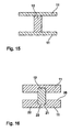
- Fig. 14 is a perspective view of a nonradiative dielectric waveguide filter according to a fourth embodiment
- Fig. 15 is a section along the line U-U of the view shown in Fig. 14
- Fig. 16 is a section along the line T-T of the view shown in Fig. 14.
- the nonradiative dielectric waveguide filter 10d of this embodiment comprises parallel upper and lower conductor plates 11 made of resin coated with metal, aluminum, or the like, and a pillar dielectric strip 12 disposed between the upper and lower conductor plates 11.
- the sections perpendicular to the signal-transmitting direction of the dielectric strip 12 have the same rectangular shape.
- Fig. 15 is a sectional view along the line U-U of the view shown in Fig. 14; and Fig. 16 is a sectional view along the line T-T of the view shown in Fig. 14.
- the LSE mode is used as a transmission mode, and setting of frequencies allows the parts where the side of the dielectric strip 12 is not covered by the conductor to be a signal-transmitting region, whereas it allows the part where the side of the same is covered by the conductor to be a cut-off region 17.
- the signal-transmitting region serves as the resonator 15 and the input-output connection means 16, and the nonradiative dielectric waveguide filter 10d serves as a band pass filter having two resonators.
- the region, in which a groove with a depth of 0.4 mm, that is, a step with a height of 0.4 mm is formed in the conductor plate is a cut-off region, whereas the region having no grooves is a signal-transmitting region. Accordingly, disposing the steps on the conductor plate to fit the dielectric strip thereinto, as shown in the above embodiment, allows the side part of the dielectric strip covered by the conductor to serve as a cut-off region, whereas that allows the side part of the same not covered by the conductor to serve as a resonator and an input-output connection means.
- the dielectric strip used in the present invention should not be limited to this.
- a dielectric strip 12a as shown in Fig. 17, which is formed by bonding dielectric layers having different specific dielectric constants together in the vertical direction
- a dielectric strip 12b as shown in Fig. 18, which is formed by bonding the same layers together in the horizontal direction, may be applicable. This permits characteristic adjustment.
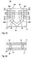
- Fig. 19 is a plan view of the duplexer according to the present invention
- Fig. 20 is a section along the line S-S of the plan view shown in Fig. 19
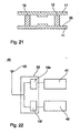
- Fig. 21 is a section along the line R-R of the plan view shown in Fig. 19.
- the duplexer 30 of the present invention comprises a nonradiative dielectric waveguide filter 10e comprising the upper and lower conductor plates 11 and the dielectric strip 12, and a nonradiative dielectric waveguide filter 10f comprising the upper and lower conductor plates 11 and the dielectric strip 12 and allowing frequencies different from those of the nonradiative dielectric waveguide filter 10e to pass through.
- These two filters 10e and 10f have the structure described in the first embodiment, in which the dielectric strip 12 is fitted into the groove 20 disposed in the upper and lower conductor plates 11; the sides of the dielectric strip 12 partially covered by the conductor walls 22 serve as the resonators 15 and the input-output connection means 16e1 16e2, 16f1, and 16f2, whereas the sides of the strip 12 not covered by the conductor walls 22 due to the formation of the lateral grooves 25 serve as the cut-off regions 17.
- One of the input-output connection means 16e1 of the nonradiative dielectric waveguide filter 10e is connected to the external transmission circuit, whereas one of the input-output connection means 16f1 of the nonradiative dielectric waveguide filter 10f is connected to the external reception circuit.
- the other input-output connection means 16e2 of the nonradiative dielectric waveguide filter 10e and the other input-output connection means 16f2 of the nonradiative dielectric waveguide filter 10f are integrated into an antenna connection means 19 so as to be connected to an antenna.
- the nonradiative dielectric waveguide filter 10e allows signals of a specified frequency to pass through
- the nonradiative dielectric waveguide filter 10f allows signals of different frequencies from those of the nonradiative dielectric waveguide filter 10e to pass through, so that it serves as a band pass duplexer.
- Fig. 22 is a schematic view of the transceiver of the embodiment.
- the transceiver 40 of the present invention comprises the duplexer 30, a transmission circuit 41, a reception circuit 42, and an antenna 43.
- the duplexer 30 is the one used in the above embodiment.
- the input-output connection means of the nonradiative dielectric waveguide filter 10e shown in Fig. 19 is connected to the transmission circuit 41, whereas the input-output connection means of the nonradiative dielectric waveguide filter 10f is connected to the reception circuit 42.
- the antenna connection means is connected to the antenna 43.
- a nonradiative dielectric waveguide filter comprising planar conductors disposed substantially parallel to each other and a dielectric strip disposed therebetween.
- the dielectric strip is fitted into the groove formed in the upper and lower conductors and, furthermore, a plurality of lateral grooves is intermittently formed therein so as to form the nonradiative dielectric waveguide filter.
- This arrangement facilitates easy manufacture of the filter without complicating production of the dielectric strip, so that production efficiency can be enhanced, reducing manufacturing cost.
- the characteristics of resonance frequency, etc. are determined by the length of the lateral groove of the conductor, a nonradiative dielectric waveguide filter which can reduce characteristic changes with respect to temperature changes is obtainable.
Landscapes
- Control Of Motors That Do Not Use Commutators (AREA)
- Waveguides (AREA)
Claims (10)
- Ein Strahlungsloser-Dielektrischer-Wellenleiter-Resonator mit folgenden Merkmalen:einem Paar gegenüberliegender planarer Leiter (11);einem dielektrischen Streifen (12), der zwischen denselben angeordnet ist;zumindest einer Resonanzregion (15); undSperrregionen (17) auf beiden Seiten des dielektrischen Streifens (12) der Resonanzregion (15) in der Signalübertragungsrichtung,dadurch gekennzeichnet, dassdie Breite des dielektrischen Streifens (12) in der zumindest einen Resonanzregion (15) gleich der Breite des dielektrischen Streifens (12) in den Sperrregionen (17) ist.
- Der Strahlungsloser-Dielektrischer-Wellenleiter-Resonator gemäß Anspruch 1, bei dem der dielektrische Streifen (12) aus einem dielektrischen Material gebildet ist, das eine einheitliche Dielektrizitätskonstante aufweist.
- Der Strahlungsloser-Dielektrischer-Wellenleiter-Resonator gemäß einem der Ansprüche 1 und 2, bei dem eine Hauptsignalübertragungsmode die LSM-Mode ist; eine erste Rille (20), die eine untere (21) und Leiterwände (22) aufweist, in einer Position angeordnet ist, in der die Leiter (11) einander gegenüberliegen; die Resonanzregion (15) durch Passen des dielektrischen Streifens (12) in die erste Rille (20) gebildet ist; und die Sperrregionen (17) entweder durch Passen des dielektrischen Streifens (12) in eine zweite Rille, die niedrigere Leiterwände (22) als diejenigen der ersten Rille (20) aufweist, oder durch Anordnen des dielektrischen Streifens (12) zwischen den Leitern (11) ohne Rillen gebildet sind.
- Der Strahlungsloser-Dielektrischer-Wellenleiter-Resonator gemäß Anspruch 3, bei dem die erste Rille (20) eine untere (21) und Leiterwände (22) mit einer spezifizierten Höhe oder höher aufweist.
- Der Strahlungsloser-Dielektrischer-Wellenleiter-Resonator gemäß einem der Ansprüche 1 und 2, bei dem eine Hauptsignalübertragungsmode die LSE-Mode ist; eine erste Rille (20), die eine untere (21) und Leiterwände (22) aufweist, in einer Position angeordnet ist, in der die Leiter (11) einander gegenüberliegen; die Sperrregionen (17) durch Passen des dielektrischen Streifens (12) in die erste Rille (20) gebildet sind; und die Resonanzregion (15) entweder durch Passen des dielektrischen Streifens (12) in eine zweite Rille, die niedrigere Leiterwände (22) als diejenigen der ersten Rille (20) aufweist, oder durch Anordnen des dielektrischen Streifens (12) zwischen den Leitern (11) ohne Rillen gebildet ist.
- Ein Strahlungsloser-Dielektrischer-Wellenleiter-Filter (10; 10a; 10b; 10c; 10d) mit folgenden Merkmalen:zwei planaren Leitern (11; 11a), die im Wesentlichen parallel zueinander angeordnet sind;einem dielektrischen Streifen (12), der im Wesentlichen die gleiche Form von Abschnitten senkrecht zu der Signalübertragungsrichtung aufweist; undEingangs-/Ausgangs-Verbindungseinrichtungen (16), die durch Anordnen des dielektrischen Streifens (12) zwischen den Leitern (11; 11a) gebildet sind;wobei die Eingangs-/Ausgangs-Verbindungseinrichtungen (16) mit dem Strahlungsloser-Dielektrischer-Wellenleiter-Resonator, der in einem der Ansprüche 1 und 2 beschrieben ist, gekoppelt sind.
- Das Strahlungsloser-Dielektrischer-Wellenleiter-Filter (10; 10a; 10b; 10c; 10d) gemäß Anspruch 6,
bei dem ein Strahlungsloser-Dielektrischer-Wellenleiter-Resonator, der zwei planare Leiter (11; 11a), die im Wesentlichen parallel zueinander angeordnet sind, und einen dielektrischen Streifen (12) aufweist, der im Wesentlichen die gleiche Form von Abschnitten senkrecht zu der Signalübertragungsrichtung aufweist, wobei der dielektrische Streifen (12) zwischen den Leitern (11; 11a) angeordnet ist, eine Resonanzregion (15) und Sperrregionen (17) aufweist; und die Eingangs-/Ausgangs-Verbindungseinrichtungen (16) eine Kopplung zu dem Strahlungsloser-Dielektrischer-Wellenleiter-Resonator herstellen;
wobei eine Hauptsignalübertragungsmode die LSM-Mode ist; eine erste Rille (20), die eine untere (21) und Leiterwände (22) aufweist, in einer Position angeordnet ist, in der die Leiter (11; 11a) einander gegenüberliegen; die Resonanzregion (15) und die Eingangs-/Ausgangs-Verbindungseinrichtungen (16) durch Passen des dielektrischen Streifens (12) in die erste Rille (20) gebildet sind; und die Sperrregionen (17) entweder durch Passen des dielektrischen Streifens (12) in eine zweite Rille, die niedrigere Leiterwände (22) als diejenigen der ersten Rille (20) aufweist, oder durch Anordnen des dielektrischen Streifens (12) zwischen den Leitern (11; 11a) ohne Rillen gebildet sind. - Das Strahlungsloser-Dielektrischer-Wellenleiter-Filter (10; 10a; 10b; 10c; 10d) gemäß Anspruch 6,
bei dem ein Strahlungsloser-Dielektrischer-Wellenleiter-Resonator, der zwei planare Leiter (11; 11a), die im Wesentlichen parallel zueinander angeordnet sind, und einen dielektrischen Streifen (12) aufweist, der im Wesentlichen die gleiche Form von Abschnitten senkrecht zu der Signalübertragungsrichtung aufweist, wobei der dielektrische Streifen (12) zwischen den Leitern (11; 11a) angeordnet ist, eine Resonanzregion (15) und Sperrregionen (17) aufweist; und die Eingangs-/Ausgangs-Verbindungseinrichtungen (16) eine Kopplung zu dem Strahlungsloser-Dielektrischer-Wellenleiter-Resonator herstellen;
bei dem eine Hauptsignalübertragungsmode die LSE-Mode ist; eine erste Rille (20), die eine untere (21) und Leiterwände (22) aufweist, in einer Position angeordnet ist, in der die Leiter (11; 11a) einander gegenüberliegen; die Sperrregionen (17) durch Passen des dielektrischen Streifens (12) in die erste Rille (20) gebildet sind; und die Resonanzregion (15) und die Eingangs-/Ausgangs-Verbindungseinrichtungen (16) entweder durch Passen des dielektrischen Streifens (12) in eine zweite Rille, die niedrigere Leiterwände (22) als diejenigen der ersten Rille (20) aufweist, oder durch Anordnen des dielektrischen Streifens (12) zwischen den Leitern (11; 11a) ohne Rillen gebildet sind. - Ein Duplexer (30) mit folgenden Merkmalen:zumindest zwei Filtern (10e, 10f);Eingangs-/Ausgangs-Verbindungseinrichtungen (16e1, 16e2, 16f1, 16f2), die mit den Filtern (10e, 10f) verbunden ist; undeiner Antennenverbindungseinrichtung (19), die mit den Filtern (10e, 10f) verbunden ist, zur gemeinsamen Verwendung;wobei zumindest eines der Filter (10e, 10f) das Strahlungsloser-Dielektrischer-Wellenleiter-Filter ist, das in den Ansprüchen 6 bis 8 beschrieben wurde.
- Ein Sende-/Empfangsgerät (40) mit folgenden Merkmalen:dem Duplexer (30), der im Anspruch 9 beschrieben ist;einer Sendeschaltung (41), die mit zumindest einer der Eingangs-/Ausgangs-Verbindungseinrichtungen des Duplexers (30) verbunden ist;einer Empfangsschaltung (42), die mit zumindest einer der Eingangs-/Ausgangs-Verbindungseinrichtungen verbunden ist, die sich von der Eingangs-/Ausgangs-Verbindungseinrichtung unterscheidet, die mit der Sendeschaltung (41) verbunden ist; undeiner Antenne (43), die mit der Antennenverbindungseinrichtung des Duplexers (40) verbunden ist.
Applications Claiming Priority (2)
| Application Number | Priority Date | Filing Date | Title |
|---|---|---|---|
| JP16235498 | 1998-06-10 | ||
| JP16235498A JP3405198B2 (ja) | 1998-06-10 | 1998-06-10 | 非放射性誘電体線路共振器、非放射性誘電体線路フィルタおよびそれを用いたデュプレクサ、通信機装置 |
Publications (2)
| Publication Number | Publication Date |
|---|---|
| EP0964471A1 EP0964471A1 (de) | 1999-12-15 |
| EP0964471B1 true EP0964471B1 (de) | 2006-08-23 |
Family
ID=15752978
Family Applications (1)
| Application Number | Title | Priority Date | Filing Date |
|---|---|---|---|
| EP99111374A Expired - Lifetime EP0964471B1 (de) | 1998-06-10 | 1999-06-10 | Nichtstrahlender dielektrischer Wellenleiterresonator, nichtstrahlendes dielektrisches Wellenleiterfilter und damit ausgerüstete Duplexer und Sender-Empfänger |
Country Status (5)
| Country | Link |
|---|---|
| US (1) | US6331809B1 (de) |
| EP (1) | EP0964471B1 (de) |
| JP (1) | JP3405198B2 (de) |
| CA (1) | CA2274269C (de) |
| DE (1) | DE69932888T2 (de) |
Families Citing this family (10)
| Publication number | Priority date | Publication date | Assignee | Title |
|---|---|---|---|---|
| DK174005B1 (da) | 2000-01-21 | 2002-04-08 | Ericsson Telefon Ab L M | Duplexfilter af bølgeledertype |
| JP3788217B2 (ja) * | 2000-09-08 | 2006-06-21 | 株式会社村田製作所 | 方向性結合器、アンテナ装置およびレーダ装置 |
| KR100399040B1 (ko) * | 2001-06-19 | 2003-09-19 | 엔알디 주식회사 | 비방사 유전체 도파관을 이용한 금속 포스트 필터 조립체 |
| KR100399041B1 (ko) * | 2001-07-03 | 2003-09-19 | 엔알디 주식회사 | 비방사 유전체 도파관을 이용한 금속 윈도우 필터 조립체 |
| US7545235B2 (en) | 2005-12-07 | 2009-06-09 | Mansour Raafat R | Dielectric resonator filter assemblies and methods |
| WO2010073554A1 (ja) * | 2008-12-26 | 2010-07-01 | 日本電気株式会社 | 帯域通過フィルタ |
| US8598960B2 (en) | 2009-01-29 | 2013-12-03 | The Boeing Company | Waveguide polarizers |
| DE102011107128A1 (de) * | 2011-07-12 | 2013-01-17 | Eads Deutschland Gmbh | Anordnung für einen nichtstrahlenden dielektrischen Rechteckwellenleiter zur unabhängigen Nutzung zweier oder mehrerer Moden zur Signal-Übertragung |
| SG188009A1 (en) * | 2011-08-26 | 2013-03-28 | Sony Corp | Waveguide network |
| CN117393984B (zh) * | 2023-11-21 | 2024-08-16 | 南通大学 | 一种正交双脊介质波导谐振器及包含该谐振器的滤波器 |
Family Cites Families (5)
| Publication number | Priority date | Publication date | Assignee | Title |
|---|---|---|---|---|
| GB1467233A (en) | 1973-02-19 | 1977-03-16 | Post Office | Dielectric waveguide filter assemblies |
| JP2897678B2 (ja) | 1995-03-22 | 1999-05-31 | 株式会社村田製作所 | 誘電体共振器及び高周波帯域通過フィルタ装置 |
| JP3166897B2 (ja) * | 1995-08-18 | 2001-05-14 | 株式会社村田製作所 | 非放射性誘電体線路およびその集積回路 |
| JP2998614B2 (ja) * | 1995-10-04 | 2000-01-11 | 株式会社村田製作所 | 誘電体線路 |
| JPH09246803A (ja) | 1996-03-01 | 1997-09-19 | Murata Mfg Co Ltd | 誘電体一体型nrd線路超電導帯域通過フィルタ装置 |
-
1998
- 1998-06-10 JP JP16235498A patent/JP3405198B2/ja not_active Expired - Fee Related
-
1999
- 1999-06-08 CA CA002274269A patent/CA2274269C/en not_active Expired - Fee Related
- 1999-06-10 US US09/330,113 patent/US6331809B1/en not_active Expired - Lifetime
- 1999-06-10 DE DE69932888T patent/DE69932888T2/de not_active Expired - Lifetime
- 1999-06-10 EP EP99111374A patent/EP0964471B1/de not_active Expired - Lifetime
Also Published As
| Publication number | Publication date |
|---|---|
| DE69932888T2 (de) | 2007-09-06 |
| JP3405198B2 (ja) | 2003-05-12 |
| DE69932888D1 (de) | 2006-10-05 |
| US6331809B1 (en) | 2001-12-18 |
| CA2274269C (en) | 2002-10-29 |
| JPH11355006A (ja) | 1999-12-24 |
| EP0964471A1 (de) | 1999-12-15 |
| CA2274269A1 (en) | 1999-12-10 |
Similar Documents
| Publication | Publication Date | Title |
|---|---|---|
| EP0856903B1 (de) | Dielektrischer Multimoden-Resonator und Eigenschafteinstellungsverfahren dafür | |
| JP3389819B2 (ja) | 誘電体導波管型共振器 | |
| EP1544939B1 (de) | Hybride Dreifachmodus keramische/metallische koaxiale Filtervorrichtung | |
| US20170263996A1 (en) | Radio-Frequency Filter | |
| US20060139127A1 (en) | Multimode dielectric resonator device, dielectric filter, composite dielectric filter and communication device | |
| US20020041221A1 (en) | Tunable bandpass filter | |
| US6445263B1 (en) | Dielectric resonator, dielectric filter, duplexer, and communication device | |
| EP0964471B1 (de) | Nichtstrahlender dielektrischer Wellenleiterresonator, nichtstrahlendes dielektrisches Wellenleiterfilter und damit ausgerüstete Duplexer und Sender-Empfänger | |
| US20080122559A1 (en) | Microwave Filter Including an End-Wall Coupled Coaxial Resonator | |
| US5192926A (en) | Dielectric filter with attenuation poles | |
| EP1052721B1 (de) | Gefaltetes Hohlleiterfilter mit gekoppelten Hohlraumresonatoren | |
| EP1079457B1 (de) | Dielektrische Resonanzvorrichtung, dielektrisches Filter, zusammengestellte dielektrische Filtervorrichtung, dielektrischer Duplexer und Kommunikationsgerät | |
| JPH0515321B2 (de) | ||
| US6201456B1 (en) | Dielectric filter, dielectric duplexer, and communication device, with non-electrode coupling parts | |
| GB2313714A (en) | Waveguide hybrid junction | |
| JP3620454B2 (ja) | 誘電体フィルタ、誘電体デュプレクサおよび通信装置 | |
| KR20050058477A (ko) | 선로 변환기, 고주파 모듈 및 통신 장치 | |
| KR100297346B1 (ko) | 유전체필터및이를이용한통신장치 | |
| US6531934B1 (en) | Dielectric resonator, dielectric filter, dielectric duplexer, oscillator, and communication device | |
| US6307449B1 (en) | Filter with spurious characteristic controlled | |
| WO2024152255A1 (en) | Resonant unit, filter comprising resonant unit, and filter assembly, antenna filter unit and radio comprising filter | |
| JPH11330816A (ja) | 非放射性誘電体線路と共振器との結合構造、およびそれを利用した発振器、フィルタ、デュプレクサ、通信機装置 | |
| JPH11330817A (ja) | 誘電体共振器装置、誘電体フィルタ、発振器および電子機器 | |
| JPS60145702A (ja) | 誘電体ろ波器 |
Legal Events
| Date | Code | Title | Description |
|---|---|---|---|
| PUAI | Public reference made under article 153(3) epc to a published international application that has entered the european phase |
Free format text: ORIGINAL CODE: 0009012 |
|
| 17P | Request for examination filed |
Effective date: 19990610 |
|
| AK | Designated contracting states |
Kind code of ref document: A1 Designated state(s): DE FR GB |
|
| AX | Request for extension of the european patent |
Free format text: AL;LT;LV;MK;RO;SI |
|
| AKX | Designation fees paid |
Free format text: DE FR GB |
|
| 17Q | First examination report despatched |
Effective date: 20040921 |
|
| GRAP | Despatch of communication of intention to grant a patent |
Free format text: ORIGINAL CODE: EPIDOSNIGR1 |
|
| GRAS | Grant fee paid |
Free format text: ORIGINAL CODE: EPIDOSNIGR3 |
|
| GRAA | (expected) grant |
Free format text: ORIGINAL CODE: 0009210 |
|
| AK | Designated contracting states |
Kind code of ref document: B1 Designated state(s): DE FR GB |
|
| REG | Reference to a national code |
Ref country code: GB Ref legal event code: FG4D |
|
| REF | Corresponds to: |
Ref document number: 69932888 Country of ref document: DE Date of ref document: 20061005 Kind code of ref document: P |
|
| EN | Fr: translation not filed | ||
| PLBE | No opposition filed within time limit |
Free format text: ORIGINAL CODE: 0009261 |
|
| STAA | Information on the status of an ep patent application or granted ep patent |
Free format text: STATUS: NO OPPOSITION FILED WITHIN TIME LIMIT |
|
| 26N | No opposition filed |
Effective date: 20070524 |
|
| GBPC | Gb: european patent ceased through non-payment of renewal fee |
Effective date: 20070610 |
|
| PG25 | Lapsed in a contracting state [announced via postgrant information from national office to epo] |
Ref country code: FR Free format text: LAPSE BECAUSE OF FAILURE TO SUBMIT A TRANSLATION OF THE DESCRIPTION OR TO PAY THE FEE WITHIN THE PRESCRIBED TIME-LIMIT Effective date: 20070511 |
|
| PG25 | Lapsed in a contracting state [announced via postgrant information from national office to epo] |
Ref country code: GB Free format text: LAPSE BECAUSE OF NON-PAYMENT OF DUE FEES Effective date: 20070610 |
|
| PG25 | Lapsed in a contracting state [announced via postgrant information from national office to epo] |
Ref country code: FR Free format text: LAPSE BECAUSE OF FAILURE TO SUBMIT A TRANSLATION OF THE DESCRIPTION OR TO PAY THE FEE WITHIN THE PRESCRIBED TIME-LIMIT Effective date: 20060823 |
|
| PGFP | Annual fee paid to national office [announced via postgrant information from national office to epo] |
Ref country code: DE Payment date: 20130605 Year of fee payment: 15 |
|
| REG | Reference to a national code |
Ref country code: DE Ref legal event code: R119 Ref document number: 69932888 Country of ref document: DE |
|
| REG | Reference to a national code |
Ref country code: DE Ref legal event code: R119 Ref document number: 69932888 Country of ref document: DE Effective date: 20150101 |
|
| PG25 | Lapsed in a contracting state [announced via postgrant information from national office to epo] |
Ref country code: DE Free format text: LAPSE BECAUSE OF NON-PAYMENT OF DUE FEES Effective date: 20150101 |