EP1052721B1 - Gefaltetes Hohlleiterfilter mit gekoppelten Hohlraumresonatoren - Google Patents
Gefaltetes Hohlleiterfilter mit gekoppelten Hohlraumresonatoren Download PDFInfo
- Publication number
- EP1052721B1 EP1052721B1 EP00109183A EP00109183A EP1052721B1 EP 1052721 B1 EP1052721 B1 EP 1052721B1 EP 00109183 A EP00109183 A EP 00109183A EP 00109183 A EP00109183 A EP 00109183A EP 1052721 B1 EP1052721 B1 EP 1052721B1
- Authority
- EP
- European Patent Office
- Prior art keywords
- filter
- pass
- resonator
- resonators
- waveguide
- Prior art date
- Legal status (The legal status is an assumption and is not a legal conclusion. Google has not performed a legal analysis and makes no representation as to the accuracy of the status listed.)
- Expired - Lifetime
Links
- 230000005540 biological transmission Effects 0.000 claims abstract description 52
- 230000008878 coupling Effects 0.000 claims description 14
- 238000010168 coupling process Methods 0.000 claims description 14
- 238000005859 coupling reaction Methods 0.000 claims description 14
- XAGFODPZIPBFFR-UHFFFAOYSA-N aluminium Chemical compound [Al] XAGFODPZIPBFFR-UHFFFAOYSA-N 0.000 claims description 2
- 229910052782 aluminium Inorganic materials 0.000 claims description 2
- 210000000554 iris Anatomy 0.000 description 23
- 230000000694 effects Effects 0.000 description 2
- 238000003780 insertion Methods 0.000 description 2
- 230000037431 insertion Effects 0.000 description 2
- 238000004088 simulation Methods 0.000 description 2
- 230000002238 attenuated effect Effects 0.000 description 1
- 230000001419 dependent effect Effects 0.000 description 1
- 238000001914 filtration Methods 0.000 description 1
- 238000012986 modification Methods 0.000 description 1
- 230000004048 modification Effects 0.000 description 1
- 238000002271 resection Methods 0.000 description 1
- 230000001629 suppression Effects 0.000 description 1
Images







Classifications
-
- H—ELECTRICITY
- H01—ELECTRIC ELEMENTS
- H01P—WAVEGUIDES; RESONATORS, LINES, OR OTHER DEVICES OF THE WAVEGUIDE TYPE
- H01P1/00—Auxiliary devices
- H01P1/20—Frequency-selective devices, e.g. filters
- H01P1/207—Hollow waveguide filters
- H01P1/211—Waffle-iron filters; Corrugated structures
Definitions
- the present invention is directed to the field of electronic filters. More particularly, the present invention provides a compact waveguide filter providing band-pass or low-pass response in the microwave frequency range.
- Waveguide filters are known in this art. There are two primary types of filters for use in the microwave frequency range (i.e. from about 2-20 GHz) -- symmetrically corrugated filters and iris filters. However, both of these types of filters suffer from many disadvantages.
- FIG. 1 of the '710 patent shows a standard E-plane corrugated structure having a uniform waveguide channel with a plurality of symmetrical corrugations. But as noted in the '710 patent, these types of corrugated filters are typically low-pass only. Such a filter typically cannot provide a band-pass response.
- the '710 patent purports to have advantages over the standard corrugated structure by forming a plurality of capacitive irises. Instead of forming a uniform waveguide channel, the '710 patent provides a series of iris structures ( Figs. 2 and 6 ), which have different heights. Although the irises and the corrugations are of different height, for any one iris or corrugation the structure is symmetrical.
- Another example of an iris filter (known as an H-plane iris filter) is shown in United States Patent No. 2,585,563 to Lewis, et al. This type of iris filter suffers from many disadvantages, however. First, it typically provides band-pass response only, i.e.
- the iris filter is typically a large structure, as the irises are generally separated along the waveguide channel by a half of a wavelength ( ⁇ g/2). Since the number of irises typically correlates to the order of the filter, when the order of the filter is high, such as 5th order or greater, the filter is very large.
- filters include resonant iris filters (as shown in United States Patent Nos. 1,788,538 to Norton and 1,849,659 to Bennett) and evanescent-mode ridged filters (as shown in United States Patent No. 4,646,039 to Saad).
- the resonant iris filter utilizes a plurality of resonant diaphragms as resonating elements that are separated by a quarter of a wavelength ( ⁇ g/4).
- the evanescent-mode ridged filter is based on a wavelength structure with a ridged cross section.
- a common problem with both of these types of filters is that they typically cannot handle high-powered signals.
- WO-A-00/55937 discloses a waveguide filter having asymmetrically corrugated resonators. Each resonator contributes one reflection zero and two transmission zeros to the frequency response of the filter. Each resonator has a pair of opposed slots which span the waveguide channel and are of different depths.
- US-A-3,597,710 discloses a waveguide band pass filter that has a series of capacitative irises that form corrugations within a rectangular waveguide.
- the irises provide a series of discontinuities but are not resonators.
- DE-A-19736367 discloses a waveguide having a series of cavities in the E-plane which do not act as resonators.
- a corrugated waveguide filter having a frequency response comprising a passband with a centre frequency
- the filter comprising: a plurality of resonators (64); and a plurality of coupling transformers (66) connecting said resonators, each coupling transformer (66) coupling respective two adjacent resonators; wherein each resonator (64) comprises a pair of extracted cavities separated by a distance (d), each of the two cavities comprising one slot (68A, 68B) with the same depth (h); wherein each resonator is operable to provide a reflection zero (76, 86) and a second order transmission zero (78, 88) to the frequency response of the filter, the reflection zero (76, 86) being within the filter passband and the second order transmission zero (78, 88) being either above or below the filter passband, and characterized in that : each coupling transformer (66) is a uniform waveguide section extending along the direction of said slots (68A, 68B) with a
- the present invention overcomes the disadvantages of presently known filters and also provides many advantages, such as: (1) compact size; (2) high-powered capability; (3) sharp roll-off on both sides of the pass-band; (4) low insertion loss; (5) wide and deep rejection response; (6) optional transformer units; and (7) either horizontal or vertical implementations.
- FIG. 1 is an E-plane cross-section and end-view of a corrugated waveguide filter 10A according to the present invention having a plurality of symmetrical resonators 16A arranged in a horizontal manner.
- the filter 10A includes interface flanges 12, quarter-wave transformer sections 14, external waveguide connections 18, and a plurality of symmetrical resonators 16A.
- the interface flanges 12 connect the waveguide 10A to external waveguide line (not shown).
- the quarter-wave transformers 14 couple the external waveguide line to the internal portion of the filter, where the waveguide channel 15 is formed, and where the filtering takes place.
- the waveguide channel 15 provides a path for electromagnetic energy flow through the filter.
- each of the resonators 16A includes a pair of closely-spaced (i.e. much less than ⁇ g/4) corrugated cavities (or slots), thus forming a coupled resonator cavity 16A.
- the structure, spacing and configuration of these corrugated resonators 16A determines the frequency response of the filter.
- the resonators 16A in Figure 1 are symmetrical in the sense that the corrugated slots that form the resonator couple extend into both of the side walls of the waveguide channel 15. In the embodiment of the invention shown in Figure 2 , the resonators are asymmetrical since the corrugated slots extend into only one of the waveguide channel 15 side walls.
- the resonators are preferably separated ("y") by a quarter of a wavelength of the central frequency of the pass-band ( ⁇ g/4) of the filter, although they could be separated by a longer or shorter distance.
- the transformer sections 14 are also preferably ⁇ g/4 in length ("x"), although they could be of a different length. Each of the transformer sections 14 contributes a reflection zero to the frequency response of the filter
- Each of the resonators 16A provides a reflection zero within the pass-band of the filter, and also provides a second-order transmission zero (i.e. two transmission zeros) on either the high-side or low-side of the pass-band.
- the resonators 16A can be of two types -- low-pass or high-pass.
- the low-pass resonators have corrugated slots (or cavities) in which the depth of the cavities is less than ⁇ g/4, and the high-pass resonators have corrugated slots in which the depth of the cavities is greater than ⁇ g/4.
- the filter 10A shown in Figure 1 provides an Nth-order bandpass response, where N is the number of resonators 16A formed in the structure. If the transformer units 14 are utilized, then the order of the filter is N+2, as each transformer 14 contributes a reflection zero within the pass-band of the filter. Because each of the internal resonators 16A also provides second-order transmission zeros either below or above the pass-band, the roll-off at the edges of the pass-band is sharp and wide.
- the filter response can be designed to be of many types, including Chebychev or maximally-flat, for example.
- Figure 2 is an E-plane cross-section and end-view of another corrugated waveguide filter 10B according to the present invention having a plurality of asymmetrical resonators 16B arranged in a horizontal manner.
- the elements of the filter in Figure 2 are the same as in Figure 1 , except that the corrugations in the waveguide channel 15 are formed on only one side wall.
- the performance of this type of filter is slightly less than the filter shown in Figure 1 , it provides many of the same advantages since the coupled resonator pairs 16B operate in the same fashion as the coupled resonator pairs 16A in Figure 1 -- i.e . each resonator 16B contributes a reflection zero within the pass-band of the filter and two transmission zeros on one side of the pass-band.
- the waveguide filters 10A, 10B are preferably made of aluminum, although other materials could be used. In addition, these filters preferably operate in the microwave region between 2 and 20 GHz, however they could easily operate at other frequencies. The filters are particularly well-suited for high-powered microwave signals.
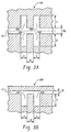
- Figure 3A is an E-plane cross-section of one of the symmetrical resonators 16A shown in Figure 1
- Figure 3B is the same for one of the asymmetrical resonators 16B shown in Figure 2
- the symmetrical resonator 16A includes a pair of extracted cavities.
- a first cavity having two extracted slots 20A, 20B, and a second cavity also having two extracted slots 20C, 20D.
- the two slots in a given cavity are separated by the waveguide channel 15, which has a dimension 2b.
- the width of the dimension 2b effects the power-handling capability of the filter.
- Each slot 20A, 20B, 20C, 20D has dimensions "h” and "s" where "h” is the depth of the slot and "s" is the width of the slot.
- the two cavities are, in turn, separated by a distance "d".
- the distance between the cavitites “d” determines the resonant frequency of the resonator couple, and hence the position of the reflection zero.
- the dimension “h” of the slots determines the position of the transmission zeros, either higher than or lower than the pass-band of the filter. If the dimension "h" is less than ⁇ g/4, then the transmission zeros an on the high-side of the pass-band, and therefore the resonator is a low-pass type. Alternately, if the dimension "h” is greater than ⁇ g/4, then the transmission zeros are on the low-side of the pass-band, and therefore the resonator is a high-pass type. For the high-pass type resonator, the distance “h” is typically between ⁇ g/4 and ⁇ g/2. The "s" dimension, as well as the "h” dimension, determine the loaded quality factor of the resonator.
- the resonator shown in Figure 3B includes two coupled cavities (or slots) 22A, 22B separated by a distance "d".
- This resonator 16B is asymmetrical in that the slots are extracted from only one side of the waveguide channel 15 sidewall.
- this resonator operates according to the same principles as that in Figure 3A .
- the distance "d” determines the location of the reflection zero within the pass-band of the filter
- the distance “h” determines the positioning of the transmission zeros (and hence whether the resonator is low-pass or high-pass)
- the distance "s" effects the loaded quality factor of the resonator.
- Figures 4 , 5 , 6A, 6B , 7A and 7B are various simulation plots of the transmission and reflection response of a waveguide filter similar to the those set forth in Figures 1 and 2 .
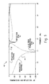
- Figure 4 is a plot showing the transmission and reflection frequency response of a low-pass resonator for use with the waveguide filter.
- Figure 5 is the same for a high-pass resonator.
- Figures 6A and 6B are plots showing, respectively, the transmission and reflection frequency response of a filter such as shown in Figures 1 or 2 , in which the resonators are all low-pass.
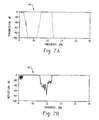
- Figures 7A and 7B are plots showing, respectively, the transmission and reflection frequency response of a filter such as shown in Figures 1 or 2 , in which the resonators are both low-pass and high-pass.
- frequency is measured on the x-axis in GHz
- frequency response is measured on the y-axis in dB.
- FIG 4 a typical response 30 for a low-pass resonator is shown.
- the reflection response 32 and the transmission response 34 are graphed together in this plot.
- This type of resonator is characterized by a slot depth -- dimension "h" -- that is less than ⁇ g/4.
- the exact depth "h” determines the position of the second-order transmission zeros 38, which, as shown in the plot, are on the high-side of the passband, around 17.5 GHz.
- the position of the reflection zero 36 is at about 12 GHz -- within the pass-band of the filter -- and its exact location is determined by the distance "d" between the pair of coupled resonator slots.
- Figure 5 shows a similar response plot 40 for a high-pass resonator. Like Figure 4 , this plot shows the reflection response 42 and the transmission response 44.
- This type of resonator is characterized by a slot depth -- dimension "h" -- that is greater than ⁇ g/4.
- the exact depth "h” determines the position of the second-order transmission zeros 48, which, as shown in the plot, axe on the low-side of the passband, around 11 GHz.
- the position of the reflection zero 48 is at about 12 GHz -- within the pass-band of the filter -- and its exact location is determined by the distance "d" between the pair of coupled resonator slots in the high-pass resonator.
- Figures 6A and 6B set forth the transmission response 50 and reflection response 52 of a waveguide filter similar to those shown in Figure 1 or 2 , in which the resonators 16A or 16B are all of the low-pass type -- i.e "h" is less than ⁇ g/4 for each of the resonators.
- the roll-off on the low-side of the pass-band (which is between about 10.5 and 12.5 GHz) is less steep than on the high-side of the pass-band due to the multiple transmission zeros contributed by the low-pass resonators.
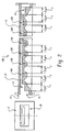
- Figure 8 is an E-plane cross-section of a corrugated waveguide filter 60 according to the present invention, including a plurality of H-stub resonators 64 arranged in a vertical manner.
- the input and output of the filter can be 1/4 wave transformer sections, similar to those shown in Figures 1 and 2 , or could be special T-shaped transformer sections 62 having an optional resonant iris element.
- Figure 8 shows a filter 60 with the T-shaped transformer sections 62. Between the transformers 62 are the plurality of H-stub resonators 64. Like Figures 1 and 2 , the number of resonators 64 determines the order of the filter. Each of the resonators 64 provides one reflection zero and a second-order transmission zero to the frequency response of the filter.
- This filter 60 can be used as a band-pass filter or a low-pass filter, depending on the configuration of the resonators and their positioning with respect to each other.
- Each of the resonators 64 is coupled together by a coupling transformer 66, which is a uniform (i.e. non-corrugated) waveguide section that is approximately ⁇ g/4 in length, although other distances are possible, including a distance of zero, in which case the resonators are just coupled together from one slot to the next.
- Quarter-wave coupling transformers 66 are used for implementations of the filter that are band-pass in order to achieve some rejection below the filter pass-band. For low-pass filter types, the coupling transformers 66 are reduced in length in order to provide more rejection on the high-side of the pass-band.
- Figure 9 is an E-plane cross-section of one of the H-stub resonators 64 shown in Figure 8 .
- the resonator 64 includes a pair of extracted cavities 68A, 68B, which are separated by a distance "d,” and connected on either side to the coupling transformers 66.
- the depth of the extracted cavities is denoted "h,” and the height of the section of waveguide coupling the resonators is denoted as "s.”
- the distance between the cavitites "d” determines the resonant frequency of the resonator couple, and hence the position of the reflection zero.
- the dimension "h” of the slots determines the position of the transmission zeros, either higher than or lower than the pass-band of the filter. If the dimension "h" is less than ⁇ g/4, then the transmission zeros are on the high-side of the pass-band, and therefore the resonator is a low-pass type. Alternately, if the dimension "h” is greater than ⁇ g/4, then the transmission zeros are on the low-side of the pass-band, and therefore the resonator is a high-pass type. For the high-pass type resonator, the distance “h” is typically between ⁇ g/4 and ⁇ g/2. The "s" dimension, as well as the "h” dimension, determine the loaded quality factor of the resonator.
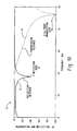
- Figure 10 is a plot 70 showing the transmission and reflection frequency response of a low-pass H-stub resonator 64, and Figure 11 is the same 80 for a high-pass resonator.
- the reflection response 72 shows the positioning of the reflection zero 76 within the pass-band of the filter, around 12 GHz, and because this is a low-pass type resonator, the transmission response 74 shows the second order transmission zero 78 on the high side of the pass-band, around 17.5 GHz.
- the reflection response 82 shows the positioning of the reflection zero 86 within the pass-band of the filter, around 11.8 GHz
- the transmission response 84 shows the second order transmission zero 88 on the low side of the pass-band, around 10.9 GHz.
- the exact position of the reflection zeros is controlled by the resonator spacing "d,” and the exact position of the second order transmission zeros is controlled by the slot depth "h.”
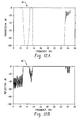
- Figures 12A and 12B are plots showing, respectively, the transmission and reflection frequency response of a waveguide filter such as shown in Figure 8 , in which the resonators are low-pass H-stub type.
- the primary pass-band of this filter is between about 12.1 and 13.8 GHz, with a spurious pass-band below about 10 GHz. Because this filter is implemented with low-pass type resonators, the roll-off above the pass-band is typically sharper and the rejection of frequencies is deeper. Both of the pass-bands (primary and spurious) can be utilized for different applications, and if the coupling transformer sections 66 are reduced in length, then the primary pass-band will merge with the spurious pass-band resulting in a low-pass filter design. Alternatively, as described below, by using a special interface transformer with a resonant iris, the spurious pass-band can be attenuated.
- This low-pass filter design provides more rejection of high frequencies than a conventional corrugated filter using the same number of extracted cavities or irises.
- the present invention provides an improved low-pass filter that is very small and capable of handling high-powered signals.
- the insertion loss of a filter according to the present invention is lower than that for a typical corrugated design.
- Figure 13 is an E-plane cross-section of an interface transformer 62 for use with a waveguide filter such as shown in Figure 8 . If the filter structure and the interface to external waveguide lines have different cross-sections, or the direction of the input/output ports is to be altered, then the interface transformer 62 can be utilized. On one side of the transformer is the connection 104 to external waveguide, and the other side is a matching stub 102 that connects to the internal waveguide channel. Although Figure 13 shows a one-step transformer, other types could be utilized with larger numbers of steps between the external waveguide and the internal connection.
- the matching stub 102 provides an additional advantage in that it provides a transmission zero to the filter's frequency response, thus providing additional rejection.
- a resonant iris 100 can be used with the transformer 62 in order to provide attenuation of the spurious pass-band in the filter's frequency response.
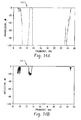
- Figures 14A and 14B are plots 110, 112 showing, respectively, the transmission and reflection frequency response of a waveguide filter such as shown in Figure 8 , using the interface transformer 62 shown in Figure 13 . As compared to Figures 12A and 12B , these figures show the additional resection in the spurious pass-band provided by the transmission zero added by the interface transformer.
- Figures 15A and 15B are plots 114, 116 showing, respectively, the transmission and reflection frequency response of a waveguide filter such as shown in Figure 8 , using the interface transformer shown in Figure 13 with an optional resonant iris 100.
- the addition of the resonant iris 100 provides a great deal of suppression on the low-side of the pass-band, thus removing the spurious pass-band from the filter's frequency response.
Landscapes
- Control Of Motors That Do Not Use Commutators (AREA)
Claims (14)
- Gewelltes Hohlleiterfilter, das einen Frequenzgang hat, der einen Durchlassbereich mit einer Mittenfrequenz umfasst, wobei das Filter Folgendes umfasst:mehrere Resonatoren (64) undmehrere Koppeltransformatoren (66), welche die Resonatoren verbinden, wobei jeder Koppeltransformator (66) jeweils zwei benachbarte Resonatoren koppelt,wobei jeder Resonator (64) ein Paar von extrahierten Hohlräumen umfasst, die durch einen Abstand (d) getrennt sind, wobei jeder der zwei Hohlräume einen Schlitz (68A, 68B) mit der gleichen Tiefe (h) umfasst,
wobei jeder Resonator funktionsfähig ist, um eine Reflexionsnullstelle (76, 86) und eine Transmissionsnullstelle zweiter Ordnung (78, 88) für den Frequenzgang des Filters bereitzustellen, wobei die Reflexionsnullstelle (76, 86) innerhalb des Filter-Durchlassbereichs liegt und die Transmissionsnullstelle zweiter Ordnung (78, 88) entweder oberhalb oder unterhalb des Filter-Durchlassbereichs liegt, und
dadurch gekennzeichnet, dass:jeder Koppeltransformator (66) eine gleichförmige Hohlleitersektion ist, die sich längs der Richtung der Schlitze (68A, 68B) erstreckt, mit einer Länge von ungefähr einem Viertel einer Wellenlänge der Mittenfrequenz des Durchlassbereichs (λg/4). - Filter nach Anspruch 1, das ferner Folgendes umfasst:eine Eingangstransformatorsektion (62) undeine Ausgangstransformatorsektion (62),wobei die Eingangs- und die Ausgangstransformatorsektion das Hohlleiterfilter an externe Hohlleiterleitungen koppeln.
- Filter nach Anspruch 2, wobei jede Transformatorsektion (62) funktionsfähig ist, um eine Reflexionsnullstelle für den Frequenzgang des Filters bereitzustellen, wobei die Reflexionsnullstelle innerhalb des Filter-Durchlassbereichs liegt.
- Filter nach Anspruch 2, wobei entweder die Eingangstransformatorsektion (62) oder die Ausgangstransformatorsektion (62) eine Resonanzblende einschließt.
- Filter nach Anspruch 1, wobei der Abstand (d) zwischen den Hohlräumen in einem bestimmten Resonator die Position der Reflexionsnullstelle für diesen Resonator bestimmt.
- Filter nach Anspruch 1, wobei die Tiefe (h) der Schlitze in einem bestimmten Resonator die Position der Transmissionsnullstelle zweiter Ordnung für diesen Resonator bestimmt.
- Filter nach Anspruch 6, wobei ein bestimmter Resonator ein Hochpass-Resonator ist, falls die Tiefe (h) der Schlitze größer ist als ein Viertel einer Wellenlänge der Mittenfrequenz des Durchlassbereichs (λg/4) des Filters.
- Filter nach Anspruch 6, wobei ein bestimmter Resonator ein Tiefpass-Resonator ist, falls die Tiefe (h) der Schlitze geringer ist als ein Viertel einer Wellenlänge der Mittenfrequenz des Durchlassbereichs (λg/4) des Filters.
- Filter nach Anspruch 1, wobei die Resonatoren alle Tiefpass-Resonatoren sind.
- Filter nach Anspruch 1, wobei das Filter wenigstens einen Tiefpass-Resonator und wenigstens einen Hochpass-Resonator umfasst.
- Filter nach Anspruch 1, wobei das Filter aus Aluminium hergestellt ist.
- Filter nach Anspruch 1, wobei das Filter zwischen etwa 2 und 20 GHz arbeitet.
- Filter nach Anspruch 1, wobei die Resonatoren H-Stumpf-Resonatoren (64) sind.
- Filter nach Anspruch 1, wobei die Ordnung des Filter-Durchlassbereichsgangs durch die Zahl der Resonatoren bestimmt wird.
Applications Claiming Priority (2)
| Application Number | Priority Date | Filing Date | Title |
|---|---|---|---|
| US09/309,406 US6169466B1 (en) | 1999-05-10 | 1999-05-10 | Corrugated waveguide filter having coupled resonator cavities |
| US309406 | 1999-05-10 |
Publications (3)
| Publication Number | Publication Date |
|---|---|
| EP1052721A2 EP1052721A2 (de) | 2000-11-15 |
| EP1052721A3 EP1052721A3 (de) | 2002-03-06 |
| EP1052721B1 true EP1052721B1 (de) | 2010-04-28 |
Family
ID=23198106
Family Applications (1)
| Application Number | Title | Priority Date | Filing Date |
|---|---|---|---|
| EP00109183A Expired - Lifetime EP1052721B1 (de) | 1999-05-10 | 2000-05-08 | Gefaltetes Hohlleiterfilter mit gekoppelten Hohlraumresonatoren |
Country Status (4)
| Country | Link |
|---|---|
| US (1) | US6169466B1 (de) |
| EP (1) | EP1052721B1 (de) |
| AT (1) | ATE466388T1 (de) |
| DE (1) | DE60044274D1 (de) |
Cited By (1)
| Publication number | Priority date | Publication date | Assignee | Title |
|---|---|---|---|---|
| WO2014039819A1 (en) * | 2012-09-07 | 2014-03-13 | Bridgewave Communications, Inc. | Metalized plastic components for millimeter wave electronics |
Families Citing this family (15)
| Publication number | Priority date | Publication date | Assignee | Title |
|---|---|---|---|---|
| DE19736367A1 (de) * | 1997-08-21 | 1999-02-25 | Bosch Gmbh Robert | Hohlleiterfilter |
| US7132909B2 (en) * | 2000-10-11 | 2006-11-07 | Paul Mack | Microwave waveguide |
| US6917266B2 (en) * | 2000-10-11 | 2005-07-12 | Paul Mack | Microwave waveguide |
| JP4173679B2 (ja) * | 2002-04-09 | 2008-10-29 | エム・イー・エス・アフティ株式会社 | Ecrプラズマ源およびecrプラズマ装置 |
| FR2848342A1 (fr) * | 2002-12-09 | 2004-06-11 | Thomson Licensing Sa | Filtre passe-bande a reponse pseudo-elliptique |
| US7606592B2 (en) * | 2005-09-19 | 2009-10-20 | Becker Charles D | Waveguide-based wireless distribution system and method of operation |
| CN103700908B (zh) * | 2013-12-09 | 2016-05-11 | 成都九洲迪飞科技有限责任公司 | 超宽带波导滤波器 |
| US9899716B1 (en) * | 2015-03-01 | 2018-02-20 | Telefonaktiebolaget Lm Ericsson (Publ) | Waveguide E-plane filter |
| CN105680123B (zh) * | 2016-01-11 | 2018-05-25 | 中国电子科技集团公司第十研究所 | Ehf频段毫米波截止波导带通滤波器 |
| KR102640203B1 (ko) * | 2016-06-24 | 2024-02-23 | 삼성전자주식회사 | 슬롯을 포함하는 광학 소자 및 이를 채용한 장치 |
| US11199661B2 (en) | 2019-10-21 | 2021-12-14 | Honeywell International Inc. | Integrated photonics vertical coupler |
| US11079542B2 (en) | 2019-10-21 | 2021-08-03 | Honeywell International Inc. | Integrated photonics source and detector of entangled photons |
| US11320720B2 (en) | 2019-10-21 | 2022-05-03 | Honeywell International Inc. | Integrated photonics mode splitter and converter |
| CN113054375A (zh) * | 2019-12-27 | 2021-06-29 | 深圳市大富科技股份有限公司 | 通信设备及其滤波器 |
| CN115000659B (zh) * | 2022-06-17 | 2022-12-16 | 华南理工大学 | 基于谐振耦合结构的波导滤波器 |
Citations (2)
| Publication number | Priority date | Publication date | Assignee | Title |
|---|---|---|---|---|
| US3597710A (en) * | 1969-11-28 | 1971-08-03 | Microwave Dev Lab Inc | Aperiodic tapered corrugated waveguide filter |
| WO2000055937A1 (en) * | 1999-03-12 | 2000-09-21 | Com Dev Limited | Waveguide filter having asymmetrically corrugated resonators |
Family Cites Families (28)
| Publication number | Priority date | Publication date | Assignee | Title |
|---|---|---|---|---|
| US1788538A (en) | 1929-04-16 | 1931-01-13 | Bell Telephone Labor Inc | Filtering circuits |
| US1849656A (en) | 1929-06-29 | 1932-03-15 | Bell Telephone Labor Inc | Transmission network |
| US2540488A (en) | 1948-04-30 | 1951-02-06 | Bell Telephone Labor Inc | Microwave filter |
| US2585563A (en) | 1949-09-17 | 1952-02-12 | Bell Telephone Labor Inc | Wave filter |
| US3046503A (en) | 1960-05-27 | 1962-07-24 | Seymour B Cohn | Broad-band waveguide filter |
| US3271706A (en) | 1964-12-07 | 1966-09-06 | Gen Electric | Microwave filter |
| GB1136158A (en) | 1966-06-10 | 1968-12-11 | Standard Telephones Cables Ltd | Improvements in or relating to waveguide filters |
| GB1129185A (en) | 1966-06-10 | 1968-10-02 | Standard Telephones Cables Ltd | Improvements in or relating to waveguide filters |
| US3634788A (en) | 1967-09-27 | 1972-01-11 | Int Standard Electric Corp | Waveguide filter |
| US3611214A (en) * | 1969-08-18 | 1971-10-05 | Varian Associates | Waveguide reflective harmonic filter |
| US3838368A (en) | 1972-06-13 | 1974-09-24 | Amana Refrigeration Inc | Waveguide filter for microwave heating apparatus |
| US3819900A (en) | 1972-06-13 | 1974-06-25 | Amana Refrigeration Inc | Waveguide filter for microwave heating apparatus |
| US3949327A (en) | 1974-08-01 | 1976-04-06 | Sage Laboratories, Inc. | Waveguide low pass filter |
| US4155056A (en) | 1977-08-25 | 1979-05-15 | Bell Telephone Laboratories, Incorporated | Cascaded grating resonator filters with external input-output couplers |
| US4492020A (en) | 1982-09-02 | 1985-01-08 | Hughes Aircraft Company | Method for fabricating corrugated microwave components |
| CA1193679A (en) | 1984-05-28 | 1985-09-17 | Abdelmegid K. Saad | Evanescent mode triple ridge lowpass harmonic filter |
| CA1194159A (en) | 1984-05-28 | 1985-09-24 | Abdelmegid K. Saad | Low pass filters with finite transmission zeros in evanescent modes |
| JPS6179301A (ja) | 1984-09-27 | 1986-04-22 | Nec Corp | 誘電体共振器帯域通過ろ波器 |
| US4749973A (en) | 1985-06-20 | 1988-06-07 | Hitachi Heating Appliances Co., Ltd. | Waveguide filter used in a microwave oven |
| JPH02190001A (ja) * | 1989-01-18 | 1990-07-26 | Nec Corp | コルゲート型ろ波器 |
| US5004993A (en) | 1989-09-19 | 1991-04-02 | The United States Of America As Represented By The Secretary Of The Navy | Constricted split block waveguide low pass filter with printed circuit filter substrate |
| US5243618A (en) | 1991-11-22 | 1993-09-07 | Hughes Aircraft Company | Cavity resonator incorporating waveguide filter |
| US5381596A (en) | 1993-02-23 | 1995-01-17 | E-Systems, Inc. | Apparatus and method of manufacturing a 3-dimensional waveguide |
| US5357591A (en) | 1993-04-06 | 1994-10-18 | Yuan Jiang | Cylindrical-wave controlling, generating and guiding devices |
| US5598300A (en) | 1995-06-05 | 1997-01-28 | Board Of Regents, The University Of Texas System | Efficient bandpass reflection and transmission filters with low sidebands based on guided-mode resonance effects |
| US5600740A (en) | 1995-06-20 | 1997-02-04 | Asfar; Omar R. | Narrowband waveguide filter |
| US5715271A (en) | 1996-08-01 | 1998-02-03 | Northern Telecom Limited | Polarization independent grating resonator filter |
| DE19736367A1 (de) * | 1997-08-21 | 1999-02-25 | Bosch Gmbh Robert | Hohlleiterfilter |
-
1999
- 1999-05-10 US US09/309,406 patent/US6169466B1/en not_active Expired - Lifetime
-
2000
- 2000-05-08 EP EP00109183A patent/EP1052721B1/de not_active Expired - Lifetime
- 2000-05-08 AT AT00109183T patent/ATE466388T1/de not_active IP Right Cessation
- 2000-05-08 DE DE60044274T patent/DE60044274D1/de not_active Expired - Lifetime
Patent Citations (3)
| Publication number | Priority date | Publication date | Assignee | Title |
|---|---|---|---|---|
| US3597710A (en) * | 1969-11-28 | 1971-08-03 | Microwave Dev Lab Inc | Aperiodic tapered corrugated waveguide filter |
| WO2000055937A1 (en) * | 1999-03-12 | 2000-09-21 | Com Dev Limited | Waveguide filter having asymmetrically corrugated resonators |
| US6232853B1 (en) * | 1999-03-12 | 2001-05-15 | Com Dev Limited | Waveguide filter having asymmetrically corrugated resonators |
Cited By (1)
| Publication number | Priority date | Publication date | Assignee | Title |
|---|---|---|---|---|
| WO2014039819A1 (en) * | 2012-09-07 | 2014-03-13 | Bridgewave Communications, Inc. | Metalized plastic components for millimeter wave electronics |
Also Published As
| Publication number | Publication date |
|---|---|
| US6169466B1 (en) | 2001-01-02 |
| EP1052721A2 (de) | 2000-11-15 |
| EP1052721A3 (de) | 2002-03-06 |
| DE60044274D1 (de) | 2010-06-10 |
| ATE466388T1 (de) | 2010-05-15 |
Similar Documents
| Publication | Publication Date | Title |
|---|---|---|
| EP1052721B1 (de) | Gefaltetes Hohlleiterfilter mit gekoppelten Hohlraumresonatoren | |
| EP1161775B1 (de) | Hohlleiterfilter mit asymmetrisch gerillten resonatoren | |
| US11031664B2 (en) | Waveguide band-pass filter | |
| US4837535A (en) | Resonant wave filter | |
| US6411181B1 (en) | Dielectric resonator, inductor, capacitor, dielectric filter, oscillator, and communication device | |
| EP2591524A1 (de) | Wellenleiterbandpassfilter mit pseudoelliptischer antwort | |
| EP0880191B1 (de) | Dielektrischer Resonator, dielektrisches Filter, Duplexer und Kommunikationsvorrichtung | |
| US6504456B2 (en) | Communication device having a spurious wave blocking circuit formed of a plural fundamental pattern | |
| US5051714A (en) | Modular resonant cavity, modular dielectric notch resonator and modular dielectric notch filter | |
| US5739734A (en) | Evanescent mode band reject filters and related methods | |
| JP2002084101A (ja) | フィルタ、マルチプレクサおよび通信装置 | |
| US12160027B2 (en) | Metallized dielectric waveguide filters having irregular shaped resonant cavities, slanted metallized openings and/or spurious coupling windows | |
| JP2641090B2 (ja) | 導波管バンドパスフィルター用二重モード空洞共振器 | |
| EP0328747B1 (de) | Modenselektives Bandpassfilter | |
| CN112563701B (zh) | 基于微扰矩形腔的双模基片集成波导滤波器 | |
| US6104262A (en) | Ridged thick walled capacitive slot | |
| JPH01152801A (ja) | 導波管帯域通過ろ波器 | |
| CA1050127A (en) | Low insertion loss waveguide filter | |
| JPH11312902A (ja) | 誘電体フィルタ、送受共用器および通信機 | |
| CA1081808A (en) | Dual mode self-equalized bandpass filters | |
| RU2848635C1 (ru) | Двенадцатизвенный волноводный фильтр СВЧ | |
| CN113036385B (zh) | 一种具有高选择性的三路滤波功率分配器 | |
| JPH0715210A (ja) | 帯域阻止濾波器 | |
| CA2298479C (en) | Spiral slot line resonator | |
| JPH0614601B2 (ja) | 帯域通過フイルタ |
Legal Events
| Date | Code | Title | Description |
|---|---|---|---|
| PUAI | Public reference made under article 153(3) epc to a published international application that has entered the european phase |
Free format text: ORIGINAL CODE: 0009012 |
|
| 17P | Request for examination filed |
Effective date: 20000509 |
|
| AK | Designated contracting states |
Kind code of ref document: A2 Designated state(s): AT BE CH CY DE DK ES FI FR GB GR IE IT LI LU MC NL PT SE |
|
| AX | Request for extension of the european patent |
Free format text: AL;LT;LV;MK;RO;SI |
|
| PUAL | Search report despatched |
Free format text: ORIGINAL CODE: 0009013 |
|
| AK | Designated contracting states |
Kind code of ref document: A3 Designated state(s): AT BE CH CY DE DK ES FI FR GB GR IE IT LI LU MC NL PT SE |
|
| AX | Request for extension of the european patent |
Free format text: AL;LT;LV;MK;RO;SI |
|
| AKX | Designation fees paid |
Free format text: AT BE CH CY DE DK ES FI FR GB GR IE IT LI LU MC NL PT SE |
|
| 17Q | First examination report despatched |
Effective date: 20071113 |
|
| GRAP | Despatch of communication of intention to grant a patent |
Free format text: ORIGINAL CODE: EPIDOSNIGR1 |
|
| GRAS | Grant fee paid |
Free format text: ORIGINAL CODE: EPIDOSNIGR3 |
|
| GRAA | (expected) grant |
Free format text: ORIGINAL CODE: 0009210 |
|
| AK | Designated contracting states |
Kind code of ref document: B1 Designated state(s): AT BE CH CY DE DK ES FI FR GB GR IE IT LI LU MC NL PT SE |
|
| REG | Reference to a national code |
Ref country code: GB Ref legal event code: FG4D |
|
| REG | Reference to a national code |
Ref country code: CH Ref legal event code: EP |
|
| REG | Reference to a national code |
Ref country code: IE Ref legal event code: FG4D |
|
| REF | Corresponds to: |
Ref document number: 60044274 Country of ref document: DE Date of ref document: 20100610 Kind code of ref document: P |
|
| REG | Reference to a national code |
Ref country code: NL Ref legal event code: VDEP Effective date: 20100428 |
|
| PG25 | Lapsed in a contracting state [announced via postgrant information from national office to epo] |
Ref country code: ES Free format text: LAPSE BECAUSE OF FAILURE TO SUBMIT A TRANSLATION OF THE DESCRIPTION OR TO PAY THE FEE WITHIN THE PRESCRIBED TIME-LIMIT Effective date: 20100808 Ref country code: SE Free format text: LAPSE BECAUSE OF FAILURE TO SUBMIT A TRANSLATION OF THE DESCRIPTION OR TO PAY THE FEE WITHIN THE PRESCRIBED TIME-LIMIT Effective date: 20100428 Ref country code: NL Free format text: LAPSE BECAUSE OF FAILURE TO SUBMIT A TRANSLATION OF THE DESCRIPTION OR TO PAY THE FEE WITHIN THE PRESCRIBED TIME-LIMIT Effective date: 20100428 |
|
| PG25 | Lapsed in a contracting state [announced via postgrant information from national office to epo] |
Ref country code: FI Free format text: LAPSE BECAUSE OF FAILURE TO SUBMIT A TRANSLATION OF THE DESCRIPTION OR TO PAY THE FEE WITHIN THE PRESCRIBED TIME-LIMIT Effective date: 20100428 Ref country code: AT Free format text: LAPSE BECAUSE OF FAILURE TO SUBMIT A TRANSLATION OF THE DESCRIPTION OR TO PAY THE FEE WITHIN THE PRESCRIBED TIME-LIMIT Effective date: 20100428 |
|
| PG25 | Lapsed in a contracting state [announced via postgrant information from national office to epo] |
Ref country code: GR Free format text: LAPSE BECAUSE OF FAILURE TO SUBMIT A TRANSLATION OF THE DESCRIPTION OR TO PAY THE FEE WITHIN THE PRESCRIBED TIME-LIMIT Effective date: 20100729 Ref country code: MC Free format text: LAPSE BECAUSE OF NON-PAYMENT OF DUE FEES Effective date: 20100531 Ref country code: CY Free format text: LAPSE BECAUSE OF NON-PAYMENT OF DUE FEES Effective date: 20100428 |
|
| REG | Reference to a national code |
Ref country code: CH Ref legal event code: PL |
|
| PG25 | Lapsed in a contracting state [announced via postgrant information from national office to epo] |
Ref country code: DK Free format text: LAPSE BECAUSE OF FAILURE TO SUBMIT A TRANSLATION OF THE DESCRIPTION OR TO PAY THE FEE WITHIN THE PRESCRIBED TIME-LIMIT Effective date: 20100428 Ref country code: PT Free format text: LAPSE BECAUSE OF FAILURE TO SUBMIT A TRANSLATION OF THE DESCRIPTION OR TO PAY THE FEE WITHIN THE PRESCRIBED TIME-LIMIT Effective date: 20100830 |
|
| PG25 | Lapsed in a contracting state [announced via postgrant information from national office to epo] |
Ref country code: CH Free format text: LAPSE BECAUSE OF NON-PAYMENT OF DUE FEES Effective date: 20100531 Ref country code: LI Free format text: LAPSE BECAUSE OF NON-PAYMENT OF DUE FEES Effective date: 20100531 Ref country code: BE Free format text: LAPSE BECAUSE OF FAILURE TO SUBMIT A TRANSLATION OF THE DESCRIPTION OR TO PAY THE FEE WITHIN THE PRESCRIBED TIME-LIMIT Effective date: 20100428 |
|
| PLBE | No opposition filed within time limit |
Free format text: ORIGINAL CODE: 0009261 |
|
| STAA | Information on the status of an ep patent application or granted ep patent |
Free format text: STATUS: NO OPPOSITION FILED WITHIN TIME LIMIT |
|
| PG25 | Lapsed in a contracting state [announced via postgrant information from national office to epo] |
Ref country code: IT Free format text: LAPSE BECAUSE OF FAILURE TO SUBMIT A TRANSLATION OF THE DESCRIPTION OR TO PAY THE FEE WITHIN THE PRESCRIBED TIME-LIMIT Effective date: 20100428 |
|
| 26N | No opposition filed |
Effective date: 20110131 |
|
| PG25 | Lapsed in a contracting state [announced via postgrant information from national office to epo] |
Ref country code: IE Free format text: LAPSE BECAUSE OF NON-PAYMENT OF DUE FEES Effective date: 20100508 |
|
| PG25 | Lapsed in a contracting state [announced via postgrant information from national office to epo] |
Ref country code: LU Free format text: LAPSE BECAUSE OF NON-PAYMENT OF DUE FEES Effective date: 20100508 |
|
| REG | Reference to a national code |
Ref country code: FR Ref legal event code: PLFP Year of fee payment: 17 |
|
| REG | Reference to a national code |
Ref country code: FR Ref legal event code: PLFP Year of fee payment: 18 |
|
| REG | Reference to a national code |
Ref country code: FR Ref legal event code: PLFP Year of fee payment: 19 |
|
| PGFP | Annual fee paid to national office [announced via postgrant information from national office to epo] |
Ref country code: DE Payment date: 20190531 Year of fee payment: 20 |
|
| PGFP | Annual fee paid to national office [announced via postgrant information from national office to epo] |
Ref country code: FR Payment date: 20190528 Year of fee payment: 20 |
|
| PGFP | Annual fee paid to national office [announced via postgrant information from national office to epo] |
Ref country code: GB Payment date: 20190529 Year of fee payment: 20 |
|
| REG | Reference to a national code |
Ref country code: DE Ref legal event code: R071 Ref document number: 60044274 Country of ref document: DE |
|
| REG | Reference to a national code |
Ref country code: GB Ref legal event code: PE20 Expiry date: 20200507 |
|
| PG25 | Lapsed in a contracting state [announced via postgrant information from national office to epo] |
Ref country code: GB Free format text: LAPSE BECAUSE OF EXPIRATION OF PROTECTION Effective date: 20200507 |
|
| P01 | Opt-out of the competence of the unified patent court (upc) registered |
Effective date: 20230525 |