EP0964507A1 - Regelkreis für einen kommutatorlosen elektrischen Motor - Google Patents
Regelkreis für einen kommutatorlosen elektrischen Motor Download PDFInfo
- Publication number
- EP0964507A1 EP0964507A1 EP99110845A EP99110845A EP0964507A1 EP 0964507 A1 EP0964507 A1 EP 0964507A1 EP 99110845 A EP99110845 A EP 99110845A EP 99110845 A EP99110845 A EP 99110845A EP 0964507 A1 EP0964507 A1 EP 0964507A1
- Authority
- EP
- European Patent Office
- Prior art keywords
- phase
- recirculation
- switches
- electronic
- circuit according
- Prior art date
- Legal status (The legal status is an assumption and is not a legal conclusion. Google has not performed a legal analysis and makes no representation as to the accuracy of the status listed.)
- Granted
Links
- 238000004804 winding Methods 0.000 claims abstract description 31
- 230000001052 transient effect Effects 0.000 claims abstract description 8
- 238000001914 filtration Methods 0.000 claims description 4
- 239000003990 capacitor Substances 0.000 claims description 3
- 239000004065 semiconductor Substances 0.000 claims description 2
- 230000000295 complement effect Effects 0.000 claims 1
- 230000001939 inductive effect Effects 0.000 description 2
- 238000010276 construction Methods 0.000 description 1
- 238000010586 diagram Methods 0.000 description 1
- 238000006073 displacement reaction Methods 0.000 description 1
- 230000005674 electromagnetic induction Effects 0.000 description 1
- 238000011084 recovery Methods 0.000 description 1
- 239000007787 solid Substances 0.000 description 1
Images

Classifications
-
- H—ELECTRICITY
- H02—GENERATION; CONVERSION OR DISTRIBUTION OF ELECTRIC POWER
- H02P—CONTROL OR REGULATION OF ELECTRIC MOTORS, ELECTRIC GENERATORS OR DYNAMO-ELECTRIC CONVERTERS; CONTROLLING TRANSFORMERS, REACTORS OR CHOKE COILS
- H02P6/00—Arrangements for controlling synchronous motors or other dynamo-electric motors using electronic commutation dependent on the rotor position; Electronic commutators therefor
- H02P6/14—Electronic commutators
-
- H—ELECTRICITY
- H02—GENERATION; CONVERSION OR DISTRIBUTION OF ELECTRIC POWER
- H02P—CONTROL OR REGULATION OF ELECTRIC MOTORS, ELECTRIC GENERATORS OR DYNAMO-ELECTRIC CONVERTERS; CONTROLLING TRANSFORMERS, REACTORS OR CHOKE COILS
- H02P6/00—Arrangements for controlling synchronous motors or other dynamo-electric motors using electronic commutation dependent on the rotor position; Electronic commutators therefor
- H02P6/08—Arrangements for controlling the speed or torque of a single motor
Definitions
- the present invention relates to a control circuit for an electric motor.
- control circuit for a half wave DC polyphase electric motor without commutator comprising:
- a brushless electric motor (the term “brushless motor” is used more widely than “motor without commutator") of the type described above is controlled by selectively supplying each phase of the motor with a direct current delivered by a supply source, for example a battery, for a time interval in which the corresponding electronic phase switch is turned on. This time interval is determined as a function of the angular position of the rotor.
- each switch is turned off, because of its inductive component, each phase releases accumulated electromagnetic energy and generates an over-voltage on the corresponding winding. It is known to provide a path for recirculation of the transient current discharged from the winding, and a circuit network for the limitation of the over-voltage on the phase.
- the arrangements adopted include, for example, a zener recirculation diode arranged between each phase and ground to bypass the phase switch when turned off and simultaneously to limit the over-voltage to a determined threshold value.
- This zener diode may alternatively be connected between the phase and the control terminal of the associated phase switch in such a way as to turn on this latter again even in the absence of the command from the driving circuit, and therefore extend the conduction of the switch possibly up to decay of the current, contemporaneously limiting the voltage to a determined value.
- Another arrangement comprises an active network adapted to drive the gate electrode of the phase switch by limiting the voltage to a slowly variable value proportional to the speed of rotation of the motor.
- the object of the invention is a control circuit for a brushless motor in which each recirculation diode is connected to the supply voltage source via a respective electronic recirculation switch selectively controllable in such a way as to allow a flow of current from each phase winding to the said source during the course of each half wave of the induced electromotive force in this winding during which the associated electronic phase switch is turned on.
- control circuit thus formed and operated, and as subsequently described, lends itself advantageously to the driving of brushless electric motors for applications in the automotive field with DC supply voltages of low value (12V) derived from the battery.
- each recirculation switch is selectively enabled to conduct by a driving circuit, thus guaranteeing a path for the transient current from the terminal of the respective phase to the supply source, at least at the moment in which the associated phase switch is turned off, and for a period sufficient to guarantee the complete decay of the current from the associated phase winding.
- phase switches are driven by a pulse width modulated (PWM) signal in the time period during which the corresponding phase is powered.
- PWM pulse width modulated
- Each recirculation switch is turned on during the course of the whole period in which the PWM modulation of the respective phase switch is controlled, and preferably for a further time interval sufficient to guarantee complete decay of the current in the phase.
- the circuit branch comprising the diode and the recirculation switch, in the intervals in which it is turned on, further behave as a voltage limiting network forcing the corresponding terminal of the phase to a voltage slightly greater than the supply voltage by a value given by the voltage established across the terminals of the diode and the switch.
- the arrangement according to the invention therefore has the advantage of allowing a high efficiency in recovering energy accumulated in the phases and of controlling the phase over-voltage with a relatively simple and low cost circuit.
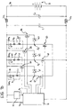
- FIG. 1a there is shown a first non-limitative embodiment of the circuit according to the invention.
- the stator phases of a brushless half-wave three-phase electric motor are constituted by the windings W1, W2, W3 disposed in a star connection, the common terminal of which is connected directly to the positive terminal of a DC supply source B.
- Each winding Wi has been shown with an equivalent circuit of series type, including a voltage generator fem i which represents the self-induced electromotive force, a resistor R i which represents the resistive component of the winding, and an inductor L i which represents the inductive component of the winding.
- phase terminals indicated as nodes A 1 , A 2 , A 3 , the three windings W1, W2, W3 are connected in series to the drain electrodes of three respective phase transistors Q1, Q2, Q3 formed as n-channel MOSFET transistors.
- the source electrodes of these transistors are connected together and coupled to ground.
- Respective recirculation branches are disposed parallel to each phase winding, and each comprises a recirculation diode, respectively D1, D2, D3, the anode of which is connected to the terminal of the corresponding phase, and a recirculation transistor Q4, Q5, Q6 respectively, in series with the diode.
- the recirculation transistors are formed as p-channel MOSFET transistors, the source electrodes of which are connected in series to the cathode of the associated diode and the drain electrodes of which are coupled to the supply source B.
- the gate electrodes of the phase transistors and the recirculation transistors are coupled to the outputs of a driving circuit 10, powered by the same source B and adapted to provide enabling signals to turn these transistors selectively and cyclically on according to predetermined manners.
- a capacitor C is provided substantially in parallel with the supply source B as a filter for the harmonic voltage components which arise across the terminals of the supply source in the particular operation of the circuit.
- An LC filter formed with inductors L F1 and L F2 and the capacitor C F is further provided across the terminals of the supply source to provide a further filtering.
- FIG. 1b A second embodiment of the control circuit is illustrated in Figure 1b. It is substantially similar to that shown in Figure 1a, except for the fact that the recirculation transistors Q4, Q5, Q6 are now formed as n-channel MOSFET transistors connected in series to the cathode of the associated diode by the drain electrodes, and coupled to the supply source B via the source electrodes.
- a voltage booster circuit 12 is arranged between the positive terminal of the supply and the driving circuit 10, which already receives supply from the source B, to provide it with a further voltage V S , greater than the battery voltage V B .
- the recirculation transistors Q4, Q5 and Q6 if made as n-channel MOSFETs and arranged as described, however, require gate control voltages greater than the maximum available voltage V B provided by a typical motor vehicle battery and present at the source electrode.
- the second supply voltage V S derived by the voltage booster circuit 12 and provided to the driving circuit 10 meets the above-mentioned requirement.
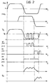
- the first graph shows the qualitative variation of the electromotive force fem 1 which develops across the phase winding W1 as a function of the angular position of the rotor of the motor.
- the second graph shows partially the qualitative variation of the analogous electromotive force fem 2 which develops across the winding W2 with a 120° electrical phase displacement.
- the third graph there is shown in broken outline the variation with time of the phase voltage V f1 present at the node A 1 with respect to ground for a theoretical "no load" operation, that is in which the phase transistor Q1 is switched off for the entire cycle of the corresponding fem 1 .
- the solid outline indicates the variation of the same voltage as a function of the driving of the transistors Q1 and Q4 plotted in the subsequent graphs.
- the transistor Q1 is turned on in correspondence with the negative half-wave of the electromotive force fem 1 by the pulse width modulated signal indicated in the graph again as Q1.
- This operating mode is known in the art for controlling the average value of the phase current I f1 in the winding W1 with precision, and is therefore not described in detail.
- the transistor Q1 is turned on (ON state) when there is detected, in a manner known per se, the passage of the rotor (not illustrated) of the motor through a given angular position.
- the conduction of the transistor Q1 can be interrupted, for example, in advance of the transistor Q2 of the phase W2 switching on, in order to permit the complete decay of the current in the winding W1 before powering the subsequent winding.
- This arrangement is not the only one possible and the system may instead advantageously operate for a short time interval with two phases powered simultaneously in such a way as to reduce the torque losses which experimentally occur in correspondence with the phase switchings because of the significant reduction in the electromagnetic induction field generated by successive phases.
- the recirculation transistor Q4 is turned on by the driving circuit at least when the corresponding transistor Q1 is turned off, for a time within the 180 electrical degrees in which the voltage fem 1 maintains the correct polarity for the generation of torque, and is turned off outside the said interval of 180 electrical degrees to prevent braking of the motor.
- phase voltage V f1 present at the node A 1 goes to a value close to the ground voltage, determined by the voltage drop between the drain of Q1 and ground.
- the recirculation diode D1 cannot be forward biased so as also to become conductive, and the phase current I f1 flows from the winding W1 towards ground.
- Schottky diodes are advantageously used as the recirculation diodes since in switching they have a faster response than p-n junction diodes and a lower voltage drop.
- the recirculation transistor Q4 can be maintained on for a time period sufficient to allow decay of the current in the associated phase winding, as shown in the drawing.
- the driving circuit 10 cyclically repeats the driving sequence described above.
- control circuit according to the invention can be used for the control of a half-wave brushless motor with a different number of phases, and in which each phase is powered in the course of the half-wave of opposite polarity from that described, depending on the mounting and circuit arrangements adopted.
Landscapes
- Engineering & Computer Science (AREA)
- Power Engineering (AREA)
- Control Of Motors That Do Not Use Commutators (AREA)
- Control Of Electric Motors In General (AREA)
Applications Claiming Priority (2)
| Application Number | Priority Date | Filing Date | Title |
|---|---|---|---|
| ITTO980502 | 1998-06-08 | ||
| IT98TO000502A ITTO980502A1 (it) | 1998-06-08 | 1998-06-08 | Circuito di controllo per motore elettrico senza collettore. |
Publications (2)
| Publication Number | Publication Date |
|---|---|
| EP0964507A1 true EP0964507A1 (de) | 1999-12-15 |
| EP0964507B1 EP0964507B1 (de) | 2010-09-08 |
Family
ID=11416833
Family Applications (1)
| Application Number | Title | Priority Date | Filing Date |
|---|---|---|---|
| EP99110845A Expired - Lifetime EP0964507B1 (de) | 1998-06-08 | 1999-06-07 | Regelkreis für einen kommutatorlosen elektrischen Motor |
Country Status (4)
| Country | Link |
|---|---|
| EP (1) | EP0964507B1 (de) |
| AT (1) | ATE480901T1 (de) |
| DE (1) | DE69942731D1 (de) |
| IT (1) | ITTO980502A1 (de) |
Cited By (2)
| Publication number | Priority date | Publication date | Assignee | Title |
|---|---|---|---|---|
| US6300740B1 (en) | 1999-02-12 | 2001-10-09 | Gate S.P.A. | Circuit for driving inductive loads |
| CN110460290A (zh) * | 2018-01-24 | 2019-11-15 | 德州仪器公司 | 用于减少电动机逆变器中的换向损失的方法 |
Citations (4)
| Publication number | Priority date | Publication date | Assignee | Title |
|---|---|---|---|---|
| US4535274A (en) * | 1983-07-20 | 1985-08-13 | Toyo Electric Co., Ltd. | Driving circuit for brushless D.C. motor |
| EP0538204A1 (de) * | 1991-10-15 | 1993-04-21 | INDUSTRIE MAGNETI MARELLI S.p.A. | Regelkreis für eine Halbwellensteuerung eines bürstenlosen Motors mit Schaltstromspitzenbegrenzung |
| JPH0638579A (ja) * | 1992-07-16 | 1994-02-10 | Nippon Densan Corp | スナバ回路 |
| DE19745312A1 (de) * | 1996-10-18 | 1998-04-23 | Papst Motoren Gmbh & Co Kg | Anteuerschaltung für einen bürstenlosen Gleichstrommotor |
-
1998
- 1998-06-08 IT IT98TO000502A patent/ITTO980502A1/it unknown
-
1999
- 1999-06-07 AT AT99110845T patent/ATE480901T1/de not_active IP Right Cessation
- 1999-06-07 DE DE69942731T patent/DE69942731D1/de not_active Expired - Lifetime
- 1999-06-07 EP EP99110845A patent/EP0964507B1/de not_active Expired - Lifetime
Patent Citations (4)
| Publication number | Priority date | Publication date | Assignee | Title |
|---|---|---|---|---|
| US4535274A (en) * | 1983-07-20 | 1985-08-13 | Toyo Electric Co., Ltd. | Driving circuit for brushless D.C. motor |
| EP0538204A1 (de) * | 1991-10-15 | 1993-04-21 | INDUSTRIE MAGNETI MARELLI S.p.A. | Regelkreis für eine Halbwellensteuerung eines bürstenlosen Motors mit Schaltstromspitzenbegrenzung |
| JPH0638579A (ja) * | 1992-07-16 | 1994-02-10 | Nippon Densan Corp | スナバ回路 |
| DE19745312A1 (de) * | 1996-10-18 | 1998-04-23 | Papst Motoren Gmbh & Co Kg | Anteuerschaltung für einen bürstenlosen Gleichstrommotor |
Non-Patent Citations (1)
| Title |
|---|
| PATENT ABSTRACTS OF JAPAN vol. 018, no. 263 (E - 1550) 19 May 1994 (1994-05-19) * |
Cited By (3)
| Publication number | Priority date | Publication date | Assignee | Title |
|---|---|---|---|---|
| US6300740B1 (en) | 1999-02-12 | 2001-10-09 | Gate S.P.A. | Circuit for driving inductive loads |
| EP1028527B1 (de) * | 1999-02-12 | 2006-05-10 | GATE S.r.l. | Schaltung zum Treiben induktiver Lasten |
| CN110460290A (zh) * | 2018-01-24 | 2019-11-15 | 德州仪器公司 | 用于减少电动机逆变器中的换向损失的方法 |
Also Published As
| Publication number | Publication date |
|---|---|
| EP0964507B1 (de) | 2010-09-08 |
| ATE480901T1 (de) | 2010-09-15 |
| ITTO980502A1 (it) | 1999-12-08 |
| DE69942731D1 (de) | 2010-10-21 |
Similar Documents
| Publication | Publication Date | Title |
|---|---|---|
| US12576733B2 (en) | Vehicle electrical system | |
| US8040094B2 (en) | Voltage clamping and energy recovery circuits | |
| US5668450A (en) | Half-wave, brushless, four-phase DC motor with bifilar windings | |
| TWI680630B (zh) | 用於逆變器的控制裝置 | |
| US9705423B1 (en) | Controlled bootstrap driver for high side electronic switching device | |
| EP0041769B1 (de) | Transistorzerhackerschaltungen | |
| JP3889445B2 (ja) | 電子整流型の高能率電気モータ | |
| EP0511392B1 (de) | Gleichstrommotor | |
| KR100565023B1 (ko) | 직류 모터용 제어 회로 | |
| CN206041860U (zh) | 电机驱动装置 | |
| EP1045501A2 (de) | Schaltung zum Ansteuern von induktiven Lasten, insbesondere für einen elektrischen Gleichstrommotor | |
| EP0964507B1 (de) | Regelkreis für einen kommutatorlosen elektrischen Motor | |
| US11750085B2 (en) | Electric device | |
| EP4175161B1 (de) | Adaptive gleichrichtung zur verhinderung von strominversion in einem motorantrieb | |
| EP1028527B1 (de) | Schaltung zum Treiben induktiver Lasten | |
| JP3515359B2 (ja) | インバータ回路 | |
| JP4736155B2 (ja) | インバータ装置 | |
| JPH0969435A (ja) | インダクタンス負荷駆動ブリッジ回路 | |
| GB2031669A (en) | Circuits for brushless dc motors | |
| EP1096658A2 (de) | Permanent erregter, zweiphasiger bürstenloser Gleichstrommotor | |
| JPH09182415A (ja) | 大電力昇圧チョッパ回路 | |
| KR101000121B1 (ko) | Bldc 전동기 제어를 위한 pwm 스위칭 방법과 이를 위한 시스템 장치 | |
| JP3241631B2 (ja) | 電力変換回路 | |
| JPH1141969A (ja) | モータ駆動用インバータのドライブ回路 | |
| CA2475473C (en) | Method of commutating an electronically commutated motor and motor for carrying out said method |
Legal Events
| Date | Code | Title | Description |
|---|---|---|---|
| PUAI | Public reference made under article 153(3) epc to a published international application that has entered the european phase |
Free format text: ORIGINAL CODE: 0009012 |
|
| AK | Designated contracting states |
Kind code of ref document: A1 Designated state(s): AT CH DE ES FR GB LI SE |
|
| AX | Request for extension of the european patent |
Free format text: AL;LT;LV;MK;RO;SI |
|
| 17P | Request for examination filed |
Effective date: 20000613 |
|
| AKX | Designation fees paid |
Free format text: AT BE CH CY DE DK ES LI |
|
| RBV | Designated contracting states (corrected) |
Designated state(s): AT CH DE ES FR GB LI SE |
|
| 17Q | First examination report despatched |
Effective date: 20071213 |
|
| GRAP | Despatch of communication of intention to grant a patent |
Free format text: ORIGINAL CODE: EPIDOSNIGR1 |
|
| RIN1 | Information on inventor provided before grant (corrected) |
Inventor name: PANGELLA, PIERFRANCO Inventor name: AVIDANO, MAURIZIO |
|
| RAP1 | Party data changed (applicant data changed or rights of an application transferred) |
Owner name: GATE S.R.L. |
|
| GRAS | Grant fee paid |
Free format text: ORIGINAL CODE: EPIDOSNIGR3 |
|
| GRAA | (expected) grant |
Free format text: ORIGINAL CODE: 0009210 |
|
| RIN1 | Information on inventor provided before grant (corrected) |
Inventor name: PANGELLA, PIERFRANCO Inventor name: AVIDANO, MAURIZIO |
|
| AK | Designated contracting states |
Kind code of ref document: B1 Designated state(s): AT CH DE ES FR GB LI SE |
|
| REG | Reference to a national code |
Ref country code: GB Ref legal event code: FG4D |
|
| REG | Reference to a national code |
Ref country code: CH Ref legal event code: EP |
|
| REF | Corresponds to: |
Ref document number: 69942731 Country of ref document: DE Date of ref document: 20101021 Kind code of ref document: P |
|
| PG25 | Lapsed in a contracting state [announced via postgrant information from national office to epo] |
Ref country code: AT Free format text: LAPSE BECAUSE OF FAILURE TO SUBMIT A TRANSLATION OF THE DESCRIPTION OR TO PAY THE FEE WITHIN THE PRESCRIBED TIME-LIMIT Effective date: 20100908 |
|
| PG25 | Lapsed in a contracting state [announced via postgrant information from national office to epo] |
Ref country code: SE Free format text: LAPSE BECAUSE OF FAILURE TO SUBMIT A TRANSLATION OF THE DESCRIPTION OR TO PAY THE FEE WITHIN THE PRESCRIBED TIME-LIMIT Effective date: 20100908 |
|
| PG25 | Lapsed in a contracting state [announced via postgrant information from national office to epo] |
Ref country code: ES Free format text: LAPSE BECAUSE OF FAILURE TO SUBMIT A TRANSLATION OF THE DESCRIPTION OR TO PAY THE FEE WITHIN THE PRESCRIBED TIME-LIMIT Effective date: 20101219 |
|
| PLBE | No opposition filed within time limit |
Free format text: ORIGINAL CODE: 0009261 |
|
| STAA | Information on the status of an ep patent application or granted ep patent |
Free format text: STATUS: NO OPPOSITION FILED WITHIN TIME LIMIT |
|
| 26N | No opposition filed |
Effective date: 20110609 |
|
| REG | Reference to a national code |
Ref country code: DE Ref legal event code: R097 Ref document number: 69942731 Country of ref document: DE Effective date: 20110609 |
|
| PGFP | Annual fee paid to national office [announced via postgrant information from national office to epo] |
Ref country code: DE Payment date: 20110830 Year of fee payment: 13 |
|
| REG | Reference to a national code |
Ref country code: CH Ref legal event code: PL |
|
| GBPC | Gb: european patent ceased through non-payment of renewal fee |
Effective date: 20110607 |
|
| REG | Reference to a national code |
Ref country code: FR Ref legal event code: ST Effective date: 20120229 |
|
| PG25 | Lapsed in a contracting state [announced via postgrant information from national office to epo] |
Ref country code: CH Free format text: LAPSE BECAUSE OF NON-PAYMENT OF DUE FEES Effective date: 20110630 Ref country code: LI Free format text: LAPSE BECAUSE OF NON-PAYMENT OF DUE FEES Effective date: 20110630 Ref country code: FR Free format text: LAPSE BECAUSE OF NON-PAYMENT OF DUE FEES Effective date: 20110630 |
|
| PG25 | Lapsed in a contracting state [announced via postgrant information from national office to epo] |
Ref country code: GB Free format text: LAPSE BECAUSE OF NON-PAYMENT OF DUE FEES Effective date: 20110607 |
|
| PG25 | Lapsed in a contracting state [announced via postgrant information from national office to epo] |
Ref country code: DE Free format text: LAPSE BECAUSE OF NON-PAYMENT OF DUE FEES Effective date: 20130101 |
|
| REG | Reference to a national code |
Ref country code: DE Ref legal event code: R119 Ref document number: 69942731 Country of ref document: DE Effective date: 20130101 |