EP0965884A2 - Phasenschiebermaske und Verfahren zu ihrer Herstellung - Google Patents
Phasenschiebermaske und Verfahren zu ihrer Herstellung Download PDFInfo
- Publication number
- EP0965884A2 EP0965884A2 EP99108176A EP99108176A EP0965884A2 EP 0965884 A2 EP0965884 A2 EP 0965884A2 EP 99108176 A EP99108176 A EP 99108176A EP 99108176 A EP99108176 A EP 99108176A EP 0965884 A2 EP0965884 A2 EP 0965884A2
- Authority
- EP
- European Patent Office
- Prior art keywords
- substrate
- transparent
- indicia
- spaces
- alignment detection
- Prior art date
- Legal status (The legal status is an assumption and is not a legal conclusion. Google has not performed a legal analysis and makes no representation as to the accuracy of the status listed.)
- Withdrawn
Links
Images



Classifications
-
- G—PHYSICS
- G03—PHOTOGRAPHY; CINEMATOGRAPHY; ANALOGOUS TECHNIQUES USING WAVES OTHER THAN OPTICAL WAVES; ELECTROGRAPHY; HOLOGRAPHY
- G03F—PHOTOMECHANICAL PRODUCTION OF TEXTURED OR PATTERNED SURFACES, e.g. FOR PRINTING, FOR PROCESSING OF SEMICONDUCTOR DEVICES; MATERIALS THEREFOR; ORIGINALS THEREFOR; APPARATUS SPECIALLY ADAPTED THEREFOR
- G03F9/00—Registration or positioning of originals, masks, frames, photographic sheets or textured or patterned surfaces, e.g. automatically
- G03F9/70—Registration or positioning of originals, masks, frames, photographic sheets or textured or patterned surfaces, e.g. automatically for microlithography
-
- H—ELECTRICITY
- H10—SEMICONDUCTOR DEVICES; ELECTRIC SOLID-STATE DEVICES NOT OTHERWISE PROVIDED FOR
- H10P—GENERIC PROCESSES OR APPARATUS FOR THE MANUFACTURE OR TREATMENT OF DEVICES COVERED BY CLASS H10
- H10P76/00—Manufacture or treatment of masks on semiconductor bodies, e.g. by lithography or photolithography
-
- G—PHYSICS
- G03—PHOTOGRAPHY; CINEMATOGRAPHY; ANALOGOUS TECHNIQUES USING WAVES OTHER THAN OPTICAL WAVES; ELECTROGRAPHY; HOLOGRAPHY
- G03F—PHOTOMECHANICAL PRODUCTION OF TEXTURED OR PATTERNED SURFACES, e.g. FOR PRINTING, FOR PROCESSING OF SEMICONDUCTOR DEVICES; MATERIALS THEREFOR; ORIGINALS THEREFOR; APPARATUS SPECIALLY ADAPTED THEREFOR
- G03F1/00—Originals for photomechanical production of textured or patterned surfaces, e.g., masks, photo-masks, reticles; Mask blanks or pellicles therefor; Containers specially adapted therefor; Preparation thereof
- G03F1/26—Phase shift masks [PSM]; PSM blanks; Preparation thereof
-
- G—PHYSICS
- G03—PHOTOGRAPHY; CINEMATOGRAPHY; ANALOGOUS TECHNIQUES USING WAVES OTHER THAN OPTICAL WAVES; ELECTROGRAPHY; HOLOGRAPHY
- G03F—PHOTOMECHANICAL PRODUCTION OF TEXTURED OR PATTERNED SURFACES, e.g. FOR PRINTING, FOR PROCESSING OF SEMICONDUCTOR DEVICES; MATERIALS THEREFOR; ORIGINALS THEREFOR; APPARATUS SPECIALLY ADAPTED THEREFOR
- G03F1/00—Originals for photomechanical production of textured or patterned surfaces, e.g., masks, photo-masks, reticles; Mask blanks or pellicles therefor; Containers specially adapted therefor; Preparation thereof
- G03F1/26—Phase shift masks [PSM]; PSM blanks; Preparation thereof
- G03F1/32—Attenuating PSM [att-PSM], e.g. halftone PSM or PSM having semi-transparent phase shift portion; Preparation thereof
-
- G—PHYSICS
- G03—PHOTOGRAPHY; CINEMATOGRAPHY; ANALOGOUS TECHNIQUES USING WAVES OTHER THAN OPTICAL WAVES; ELECTROGRAPHY; HOLOGRAPHY
- G03F—PHOTOMECHANICAL PRODUCTION OF TEXTURED OR PATTERNED SURFACES, e.g. FOR PRINTING, FOR PROCESSING OF SEMICONDUCTOR DEVICES; MATERIALS THEREFOR; ORIGINALS THEREFOR; APPARATUS SPECIALLY ADAPTED THEREFOR
- G03F1/00—Originals for photomechanical production of textured or patterned surfaces, e.g., masks, photo-masks, reticles; Mask blanks or pellicles therefor; Containers specially adapted therefor; Preparation thereof
- G03F1/38—Masks having auxiliary features, e.g. special coatings or marks for alignment or testing; Preparation thereof
- G03F1/42—Alignment or registration features, e.g. alignment marks on the mask substrates
-
- G—PHYSICS
- G03—PHOTOGRAPHY; CINEMATOGRAPHY; ANALOGOUS TECHNIQUES USING WAVES OTHER THAN OPTICAL WAVES; ELECTROGRAPHY; HOLOGRAPHY
- G03F—PHOTOMECHANICAL PRODUCTION OF TEXTURED OR PATTERNED SURFACES, e.g. FOR PRINTING, FOR PROCESSING OF SEMICONDUCTOR DEVICES; MATERIALS THEREFOR; ORIGINALS THEREFOR; APPARATUS SPECIALLY ADAPTED THEREFOR
- G03F7/00—Photomechanical, e.g. photolithographic, production of textured or patterned surfaces, e.g. printing surfaces; Materials therefor, e.g. comprising photoresists; Apparatus specially adapted therefor
- G03F7/70—Microphotolithographic exposure; Apparatus therefor
- G03F7/70216—Mask projection systems
- G03F7/70283—Mask effects on the imaging process
Definitions
- This invention relates generally to phase shift masks and more particularly to alignment detection indicia formed on such masks.
- phase shift masks are used to pattern semiconductors with submicron delineations.
- interference of light rays is used to provide a proper mask effect.
- the phase of the exposed light at the target is controlled such that bright areas are preferably formed 180 degrees out of phase with each other. Dark areas are thus produced between the bright areas by destructive interference.
- a phase shift mask is constructed with a repetitive pattern formed on three different distinct layers of material.
- An opaque layer such as chrome, provides areas that allow no light transmission (i.e., a highly light reflective layer, or surface).
- a first transparent layer such as quartz, provides areas which allow close to 100% of the light to pass through.
- a transparent phase shifting layer such as areas etched a predetermined distance into the quartz, provides areas which allow close to 100% of the light to pass through but phase shifted 180 degrees from the light passing through the first transparent layer.
- the first transparent layer and the transparent phase shifting layer are positioned such that light rays diffracted through each area are canceled out in a darkened area between them. This creates a pattern of dark and bright areas which can be used to clearly delineate desired features on the semiconductor wafer.
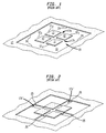
- phase shifting mask is formed by providing a quartz substrate 10 (FIGS. 1, 1A and 1B) having a chrome layer 12 formed on an upper surface thereof.
- a pattern of the described first transparent regions 16 and a first step in forming the transparent phase shifting regions 18 is etched (i.e., "written") into the chrome 12 to expose underlying top surface regions 14 of the quartz 10, as shown in FIGS. 1, 1A and 1B. It is noted that also written into the chrome 12 with the pattern is a first portion of an alignment detection region 20.
- the first portion of the alignment detection region 20 has a square chrome-quartz interface 24 with four, centrally disposed, square chrome patches 12 1 -12 4 arranged to form a cross-shaped region (i.e., a pair of intersection lines 17a, 17b) between the four square patches 12 1 -12 4 .
- the pattern of transparent phase shifting regions 18 is completed by etching the pattern of transparent phase shifting regions 18 formed in the first writing step (FIGS. 1. 1A, and 1B) into the underlying, upper surface regions, of the quartz 10 to form recesses 25 into the quartz 10, as shown in FIGS. 2, 2A and 2B. It is also noted that during this second writing step, a cross formed by lines 17'a, 17'b is etched into the upper surface portion of the quartz 10 of region 20, as shown in FIGS. 2A, 2B and 2. It is noted that if the two writing steps produce the transparent phase shifting regions 18 in proper alignment with the first transparent regions 16 the two crosses (i.e., the cross formed by lines 17a, 17b in the first write step, FIG.
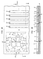
- the amount of misalignment is determined by passing a light, not shown, through a slit 21 and moving the slit 21 across the surface of the alignment detection region 20 in two steps for each of two orthogonal directions, i.e., the X direction and the Y direction indicated in FIG. 2A.
- the slit 21 is passed over the surface of the alignment detection region 20 along a first region (i.e., SCAN REGION 1) which passes over the central portion of the alignment detection region 20, i.e., over the four chrome patches 12 1 -12 4 .
- the amount of light reflected by the surface of the alignment detection region 20 is detected and a voltage representative of the amount of such reflected light is produced as a function of time or distance along the alignment detection region 20, as shown in FIG. 2C.
- the light is first reflected by the chrome surface bordering the alignment detection region 20, then by etched and un-etched surface portions of the quartz 10, then by the surfaces of the chrome patches 12 1 -12 4 , then by the un-etched surface of the quartz 10 providing line 17a and then the reflections from the surfaces repeat in a symmetrical manner.
- the voltage produced by such reflections in scanning SCAN REGION 1 is shown in FIG. 2C. It is noted that the level of the voltage has a first transition A at interface 24, a second transition B at the interface 36 between the leading edges of two patches 12 2 and 12 3 and etched quartz, a third transition C at the interface 40 between the trailing edges of the two patches 12 2 and 12 3 and the un-etched surface of the quartz 10 forming line 17a of the cross, a fourth transition D at the interface 40' between the leading edges of the two patches 12 1 and 12 4 and the un-etched surface of the quartz 10 forming the line 17a of the cross, a fifth transition at the interface 36' between the trailing edges of patches 12 1 , 12 4 and the un-etched quartz, and a sixth transition G at the interface 24.
- the slit 21, or here pair of slits 21, is passed over the surface of the alignment detection region 20 along a pair of second regions (i.e, SCAN REGION 2) each of which pass over the outer peripheral portion of the alignment detection region 20, i.e., over the surface of the un-etched quartz from line 17'a, then over the surface of the etched quartz and then over the surface of the un-etched quartz.
- the amount of light reflected by the surface of the alignment detection region 20 is detected and a voltage representative of the amount of such reflected light is produced, as shown in FIG. 2D as a function of time or distance along the alignment detection region 20.
- the voltage has a first transition H at the interface 24, a second transition I at the interface 42 between the un-etched and etched quartz 10 forming the leading edge of line 17'a, a third transition J at the interface 42' between the un-etched and etched quartz 10 forming the trailing edge of line 17'a, and a fourth transition K at the interface 24.
- a first notch 50 in the voltage level produced during scanning the SCAN REGION 1 (FIG. 2C) is produced between transitions C and D when from scanning the line 17a of the cross formed during the first write the scan and second notch 52 in the voltage level produced during scanning the SCAN REGION 2 (FIG. 2D) is produced between transitions I and J when from scanning the line 17'a of the cross formed during the second write.
- the line 17a was produced during the same write step as the first transparent regions 16 and line 17'a was produced during the same write as the transparent phase shifting regions 18, if the first transparent portions 16 formed during the first write are properly aligned with the transparent phase shifting portions 18 completed in the second write, the notches 50, 52 will be aligned (i.e, centered) with respect to each other.
- the amount of deviation between the centers of the voltages notches 50, 52 provides an indication of the misalignment in the X direction.
- the two scanning steps are also provided along the Y direction to thereby provide a Y misalignment measurement.
- the scan in SCAN REGION 2 over the un-etched portion of the quartz surface must be sufficiently long to provide a relatively constant signal level against which reflections from the etched portion of the surface can be readily detected.
- a relatively large area of the underlying silicon semiconductor material will be exposed by light passing through the quartz.
- these large exposed areas result in relatively large trenches being formed in the silicon.
- These trenches must be at least partially filled and contaminants may become somewhat captured in the trench during a trench filling process. However, the contaminants may become loose and release thereof may adversely effect the devices being fabricated.
- a phase shifting mask having a transparent substrate with an opaque material disposed on the surface of the substrate.
- the reflective material is configured to provide a first alignment detection indicia on a first portion of the surface.
- a second alignment detection indicia is distributed among a plurality of spaced regions of a second surface portion of the substrate.
- a phase shifting mask in accordance with another feature of the invention, includes a transparent substrate having an opaque material on portions of a surface of the substrate. A space is provided in the reflective material on a first surface portion of the substrate to provide a first alignment detection indicia. A plurality of spaces is provided in the opaque material on a second portion of the surface, each one of the plurality of spaces having therein a transparent indicia. The transparent indicia in the plurality of spaces provide a second alignment detection indicia.
- a phase shifting mask having an alignment detection region, a plurality of first transparent regions, and a plurality of transparent phase shifting regions.
- the mask has a transparent substrate with an opaque material disposed on selected portions of a surface of the substrate.
- the opaque material disposed on a first portion of the surface of the substrate has a space therein, such space providing a first alignment detection indicia for the alignment detection region.
- the opaque material disposed on a second portion of the surface of the substrate has a plurality of spaces therein, the spaces in the second region. Each one of the spaces has therein a transparent indicia.
- the transparent indicia in the plurality of spaces provide a second alignment detection indicia for the alignment detection region.
- phase shift mask With such an arrangement, relatively little transparency is provided by the alignment detection region of the phase shift mask thereby reducing the size of any trenches which may be formed in a silicon wafer being fabricated by the phase shift mask.
- a phase shifting mask having an alignment region, a plurality of first transparent regions, and a plurality of transparent phase shifting regions.
- the mask includes a transparent substrate having an opaque material disposed on selected portions of a surface of the substrate.
- the opaque material disposed on a first portion of the surface of the substrate has a cross-shaped space therein to expose an underlying portion of the surface of the substrate.
- a first line of the cross-shaped space provides a first one of a pair of first alignment detection indicia for the alignment detection region.
- a second line of the cross-shaped space provides a second one of the pair of first alignment detection indicia for the alignment detection region.
- the opaque material disposed on each one of a pair of second portions of the surface of the substrate has a plurality of spaces therein. Each one of the spaces in the second regions expose an underling portion of the surface of the substrate.
- the spaces in a first one of the second regions are parallel to the first line of the cross-shaped space and the spaces in a second one of the second regions are parallel to the second line of the cross-shaped space.
- a pair of the second alignment detection indicia is provided.
- a first one of the pair of the second alignment detection indicia includes a plurality of first transparent indicia, each one thereof being disposed in a corresponding one of the spaces in the first one of the second regions.
- a second one of the pair of the second alignment detection indicia includes a plurality of second transparent indicia, each one thereof being disposed in a corresponding one of the spaces in the second one of the second regions.
- the plurality of first transparent indicia provide a first one of a pair of second alignment detection indicia for the alignment detection region and the plurality of second transparent indicia provide the second one of a pair of second alignment direction indicia for the alignment detection region.
- each one of the plurality of transparent phase shifting regions and each one of the etched indicia comprise a recess etched into a portion of the surface of the substrate.
- the first and second lines of the cross-shaped space are disposed orthogonal to each other.
- the alignment detection region comprises four quadrants, a first one of the quadrants provides the first portion of the surface of the substrate, a second one of the quadrants provides a first one of the pair of second portions of the surface of the substrate, and a third one of the quadrants provides the second one of the pair of second portions of the surface of the substrate.
- the second and third quadrants are disposed adjacent to sides of the first quadrant.
- the spaces are elongated, being, after projection onto the substrate, less than a micron in width and several microns in length.
- a method for forming a phase shifting mask.
- the method includes providing a transparent substrate with an opaque material on a surface of the substrate.
- the opaque material is patterned into a first alignment detection indicia on a first region of the surface, a plurality of spaces in a second portion of the surface to expose a plurality of underlying porions of the surface of the substrate and first transparent regions in a third region of the surface.
- a second alignment detection indicia is formed along with phase shifting regions, such phase shifting regions being interleaved with the first transparent regions, such second alignment detection indicia being distributed among the plurality of spaced regions in the second portion of the surface.
- a method for determining alignment of a first transparent region and a phase shifting region of a phase shifting mask.
- the method includes providing a transparent substrate with an opaque material on a surface of the substrate.
- the opaque material is patterned into a first alignment detection indicia on a first region of the surface, a plurality of spaces in a second portion of the surface to expose a plurality of underlying portions of the surface of the substrate and first transparent regions in a third region of the surface.
- a second alignment detection indicia is formed together with phase shifting regions, such phase shifting regions being interleaved with the first transparent regions, such second alignment detection indicia being distributed among a plurality of spaced regions of the second portion in the surface.
- the first and second portions of the surface of the substrate are scanned to produce signals representative of energy reflected by the first and second alignment detection indicia.
- the produced signals are scanned to determine a spatial deviation between the first and second alignment detection indicia.
- a phase shifting mask 100 having an alignment region 102, a plurality of first transparent regions 104 interleaved with a plurality of transparent phase shifting regions 106.
- the mask 100 includes a transparent substrate 109, here quartz.
- An opaque material 110 here a reflecting material such as chrome, is disposed on selected portions of an upper surface 112 of the substrate 109.
- the opaque material 110 disposed on a first portion 114 of the surface 112 of the substrate 109 has a cross-shaped space 116 formed therein to expose an underlying portion of the surface 112 of the substrate 109.
- a first line 118 of the cross-shaped space 116 provides a first one of a pair of first alignment detection indicia for the alignment detection region 102.
- a second line 120 of the cross-shaped space 116 provides a second one of the pair of first alignment detection indicia for the alignment detection region 120.
- the opaque material 110 disposed on each one of a pair of second regions 122a, 122b of the surface 112 of the substrate 109 has a plurality of spaces 124a, 124b, respectively, formed therein. Each one of the spaces 124a, 124b in the second regions 122a, 122b expose an underling portion of the surface 112 of the substrate 109.
- the spaces 124a in the a first one of the second portions are parallel to the first line 118 of the cross-shaped space 116 and the spaces 124b in a second one of the second portions (i.e., region 122b) are parallel to the second line 120 of the cross-shaped space 116.
- a second alignment direction indicia is provided for the alignment detection region 102 in the second regions 122a, 122b during formation of the transparent phase shifting regions 106.
- the phase shifting regions 106 are formed as recesses 129 formed in the surface 112 of substrate 109, as shown in FIG. 6.
- recesses 130a, 130b are etched into the spaces 124a, 124b formed in the opaque material 110 in regions 122a, 122b, respectively.
- the recesses 130a will be disposed along the line 120 of cross region 116 and the recesses 130b will be disposed along line 118 of cross region 116.
- a pair of the plurality of transparent indicia is provided by the recesses 130a, 130b, respectively.
- Each one of the transparent indicia 130a in a first one of the pair thereof is disposed in a corresponding one of the spaces 124a in the first one of the second regions 122a and each one of the transparent indicia 130b in a second one of the pair thereof is disposed in a corresponding one of the spaces 124b in the second one of the second region 122b.
- the transparent indicia 130a in the first one of the pair thereof provide a first one of a pair of second alignment direction indicia for the alignment detection region 102 and the transparent indicia 130b in a second one of the pair thereof provide a second one of a pair of second alignment direction indicia for the alignment detection region 102.
- the first and second lines 116, 118 of the cross-shaped space 116 are orthogonal to each other.
- the alignment detection region 102 comprises four quadrants. A first one of the quadrants is first region 114, a second one of the quadrants is the first one of the pair of second regions 122a, and a third one of the quadrants is the second one of the pair of second regions 122b. The second and third quadrants are disposed adjacent to sides of the first quadrant.
- the spaces 122a, 122b are elongated.
- the spaces 122a, 122b are, after projection onto the substrate, less than a micron in width, here 0.5 microns in width.
- the spaces 122a, 122b are, after projection onto the substrate, several microns in length, here about 9 microns in length.
- the method includes providing the transparent substrate 109 with the opaque material 110 on the surface 112 of the substrate 109.
- the opaque material 110 is patterned on selected portions of the surface 112 of the substrate 109. More particularly, the opaque material 110 is patterned on the first region 114 of the surface 112 of the substrate 109 with the cross-shaped space 116, with the spaces 124a, 124b formed in regions 122a, 122b, respectively, with the spaces for the first transparent regions 104 and with the spaces 106' interleaved with the spaces for the first transparent regions 104 to expose an underlying portion of the surface 112 of the substrate 109.
- the transparent phase shifting regions 106 are completed and, during the same step, the pair of second alignment detection indicia 130a, 130b (FIGS. 5 and 6) are written, i.e., formed by etching recesses into portions of the surface 112 of substrate 109.
- a method detects alignment of first transparent regions 104 and transparent phase shifting regions 106 of the phase shifting mask 100.
- the first region 104 is scanned along the X direction with a slit, such as slit 120 in FIG. 2A, to produce, during such scan, a voltage representative of energy reflected by the reflective material 110 and by the line 118. It is noted that voltage will have a notch therein when the scanning slot passes over the line 118, i.e., one of the pair of first alignment detection indicia.
- the region 122b is scanned in the X direction by the slit to produce, during such scan, a voltage representative of energy reflected by the reflective material 110, the un-etched surface 112 exposed by spaces 124b and by the recesses 130b in such spaces 124b. It is noted that a notch will be produced in the voltage when the scan passes over line spaces 124b, i.e., one of the pair of second alignment detection indicia. It is noted that the combination of the chrome stripes and the un-etched quartz therebetween provide a composite, stable reflection reference background against which the reflections from the line formed by the etched quartz can be discriminated against.
- the two scans are then repeated along the Y axis over region 114 and then over region 122a to produce a second pair of voltages with notches therein when such scans are over line 120 and the recesses 130a.
- the voltages are processed to determine, form the notches therein, any spatial deviation between the first and second alignment detection indicia.
Landscapes
- Physics & Mathematics (AREA)
- General Physics & Mathematics (AREA)
- Preparing Plates And Mask In Photomechanical Process (AREA)
- Exposure And Positioning Against Photoresist Photosensitive Materials (AREA)
- Exposure Of Semiconductors, Excluding Electron Or Ion Beam Exposure (AREA)
Applications Claiming Priority (2)
| Application Number | Priority Date | Filing Date | Title |
|---|---|---|---|
| US09/098,785 US6042972A (en) | 1998-06-17 | 1998-06-17 | Phase shift mask having multiple alignment indications and method of manufacture |
| US98785 | 1998-06-17 |
Publications (2)
| Publication Number | Publication Date |
|---|---|
| EP0965884A2 true EP0965884A2 (de) | 1999-12-22 |
| EP0965884A3 EP0965884A3 (de) | 2000-04-05 |
Family
ID=22270881
Family Applications (1)
| Application Number | Title | Priority Date | Filing Date |
|---|---|---|---|
| EP99108176A Withdrawn EP0965884A3 (de) | 1998-06-17 | 1999-04-26 | Phasenschiebermaske und Verfahren zu ihrer Herstellung |
Country Status (6)
| Country | Link |
|---|---|
| US (1) | US6042972A (de) |
| EP (1) | EP0965884A3 (de) |
| JP (1) | JP2000019716A (de) |
| KR (1) | KR100598258B1 (de) |
| CN (1) | CN1146019C (de) |
| TW (1) | TW413843B (de) |
Cited By (2)
| Publication number | Priority date | Publication date | Assignee | Title |
|---|---|---|---|---|
| WO2001013176A1 (en) * | 1999-08-02 | 2001-02-22 | Micron Technology, Inc. | Methods of determining alignment in the forming of phase shift regions in the fabrication of a phase shift mask |
| EP1312981A3 (de) * | 2001-09-06 | 2004-10-06 | Dai Nippon Printing Co., Ltd. | Durchsichtiges Substrat mit einer Zeichen enthaltenden Zone sowie Verfahren zur Erzeugung der Zeichen |
Families Citing this family (11)
| Publication number | Priority date | Publication date | Assignee | Title |
|---|---|---|---|---|
| JP4860023B2 (ja) * | 2000-01-26 | 2012-01-25 | ルネサスエレクトロニクス株式会社 | フォトマスク |
| US6416909B1 (en) * | 2000-07-18 | 2002-07-09 | Chartered Semiconductor Manufacturing Ltd. | Alternating phase shift mask and method for fabricating the alignment monitor |
| US20030147077A1 (en) * | 2002-02-05 | 2003-08-07 | Infineon Technologies North America Corp. | Mask alignment method |
| KR100450674B1 (ko) * | 2002-03-12 | 2004-10-01 | 삼성전자주식회사 | 포토 마스크, 그 제조 방법 및 이를 이용한 웨이퍼 노광설비의 광학적 특성을 공정 중에 측정하는 방법 |
| US7909396B2 (en) * | 2004-01-08 | 2011-03-22 | Audiovox Corporation | Automobile entertainment system |
| US7396617B2 (en) * | 2004-06-14 | 2008-07-08 | Photronics, Inc. | Photomask reticle having multiple versions of the same mask pattern with different biases |
| US7435533B2 (en) * | 2004-06-14 | 2008-10-14 | Photronics, Inc. | Method of forming a semiconductor layer using a photomask reticle having multiple versions of the same mask pattern with different biases |
| US9005848B2 (en) * | 2008-06-17 | 2015-04-14 | Photronics, Inc. | Photomask having a reduced field size and method of using the same |
| US9005849B2 (en) * | 2009-06-17 | 2015-04-14 | Photronics, Inc. | Photomask having a reduced field size and method of using the same |
| JP2015204351A (ja) * | 2014-04-14 | 2015-11-16 | セイコーエプソン株式会社 | 感光膜の設置方法、半導体装置の製造方法、電気光学装置および電子機器 |
| TWI710821B (zh) * | 2019-06-04 | 2020-11-21 | 緯創資通股份有限公司 | 具有對位校準圖樣的面板裝置 |
Family Cites Families (11)
| Publication number | Priority date | Publication date | Assignee | Title |
|---|---|---|---|---|
| JP2666859B2 (ja) * | 1988-11-25 | 1997-10-22 | 日本電気株式会社 | 目合せ用バーニヤパターンを備えた半導体装置 |
| KR970010666B1 (ko) * | 1993-12-27 | 1997-06-30 | 현대전자산업 주식회사 | 반도체 소자의 패턴 중첩오차 측정방법 |
| WO1996004592A1 (en) * | 1994-08-02 | 1996-02-15 | Philips Electronics N.V. | Method of repetitively imaging a mask pattern on a substrate |
| US5477058A (en) * | 1994-11-09 | 1995-12-19 | Kabushiki Kaisha Toshiba | Attenuated phase-shifting mask with opaque reticle alignment marks |
| US5478679A (en) * | 1994-11-23 | 1995-12-26 | United Microelectronics Corporation | Half-tone self-aligning phase shifting mask |
| KR970016756A (ko) * | 1995-09-07 | 1997-04-28 | 김광호 | 하프톤 위상반전마스크 |
| KR0172790B1 (ko) * | 1995-09-18 | 1999-03-20 | 김영환 | 위상반전 마스크 및 그 제조방법 |
| KR0156422B1 (ko) * | 1995-10-05 | 1999-02-01 | 김광호 | 반도체장치 제조용 레티클 |
| KR100215850B1 (ko) * | 1996-04-12 | 1999-08-16 | 구본준 | 하프톤 위상 반전 마스크 및_그제조방법 |
| JPH1032156A (ja) * | 1996-07-15 | 1998-02-03 | Mitsubishi Electric Corp | 位相シフトマスクを用いた露光装置およびパターン形成方法 |
| US5792578A (en) * | 1997-01-13 | 1998-08-11 | Taiwan Semiconductor Manufacturing Company Ltd. | Method of forming multiple layer attenuating phase shifting masks |
-
1998
- 1998-06-17 US US09/098,785 patent/US6042972A/en not_active Expired - Lifetime
-
1999
- 1999-04-22 TW TW088106428A patent/TW413843B/zh not_active IP Right Cessation
- 1999-04-26 EP EP99108176A patent/EP0965884A3/de not_active Withdrawn
- 1999-06-14 JP JP16709199A patent/JP2000019716A/ja not_active Withdrawn
- 1999-06-17 KR KR1019990022715A patent/KR100598258B1/ko not_active Expired - Fee Related
- 1999-06-17 CN CNB991086333A patent/CN1146019C/zh not_active Expired - Fee Related
Cited By (4)
| Publication number | Priority date | Publication date | Assignee | Title |
|---|---|---|---|---|
| WO2001013176A1 (en) * | 1999-08-02 | 2001-02-22 | Micron Technology, Inc. | Methods of determining alignment in the forming of phase shift regions in the fabrication of a phase shift mask |
| US6395432B1 (en) | 1999-08-02 | 2002-05-28 | Micron Technology, Inc. | Methods of determining processing alignment in the forming of phase shift regions |
| EP1312981A3 (de) * | 2001-09-06 | 2004-10-06 | Dai Nippon Printing Co., Ltd. | Durchsichtiges Substrat mit einer Zeichen enthaltenden Zone sowie Verfahren zur Erzeugung der Zeichen |
| US7070907B2 (en) | 2001-09-06 | 2006-07-04 | Dai Nippon Printing Co., Ltd. | Substrate having character/symbol section and processing method of character/symbol section |
Also Published As
| Publication number | Publication date |
|---|---|
| CN1146019C (zh) | 2004-04-14 |
| EP0965884A3 (de) | 2000-04-05 |
| CN1244030A (zh) | 2000-02-09 |
| TW413843B (en) | 2000-12-01 |
| US6042972A (en) | 2000-03-28 |
| JP2000019716A (ja) | 2000-01-21 |
| KR20000006250A (ko) | 2000-01-25 |
| KR100598258B1 (ko) | 2006-07-07 |
Similar Documents
| Publication | Publication Date | Title |
|---|---|---|
| US6042972A (en) | Phase shift mask having multiple alignment indications and method of manufacture | |
| US5982044A (en) | Alignment pattern and algorithm for photolithographic alignment marks on semiconductor substrates | |
| US6645823B2 (en) | Reticle and method of fabricating semiconductor device | |
| US5936738A (en) | Focus monitor for alternating phase shifted masks | |
| US6888261B2 (en) | Alignment mark and exposure alignment system and method using the same | |
| KR20000029347A (ko) | 위치정렬을 검출하는 마크를 구비한 레티클과 위치정렬검출방법 | |
| KR101489329B1 (ko) | 포토키 및 이를 이용한 반도체 소자의 제조방법 | |
| KR0172790B1 (ko) | 위상반전 마스크 및 그 제조방법 | |
| US7056625B2 (en) | Focus detection structure | |
| US5670281A (en) | Masks and methods of forming masks which avoid phase conflict problems in phase shifting masks | |
| JPH09148242A (ja) | X線マスクとその製造方法 | |
| KR100392744B1 (ko) | 반도체 장치, 그 제조에 이용하는 포토마스크, 및 그 중첩정밀도 향상 방법 | |
| US7754396B2 (en) | Mask with focus measurement pattern and method for measuring focus value in exposure process using the same | |
| HK1022023A (en) | Phase shift mask and methods of manufacture | |
| US5658696A (en) | Phase shift mask | |
| KR101067860B1 (ko) | 멀티오버레이 측정마크 및 그 형성 방법 | |
| KR100495920B1 (ko) | 반도체 장치의 웨이퍼 정렬용 정렬 마크 | |
| KR100450674B1 (ko) | 포토 마스크, 그 제조 방법 및 이를 이용한 웨이퍼 노광설비의 광학적 특성을 공정 중에 측정하는 방법 | |
| US6524751B1 (en) | Reticle design for alternating phase shift mask | |
| GB2361551A (en) | Reticle | |
| JPH06324475A (ja) | レチクル | |
| KR0172789B1 (ko) | 위상반전 마스크의 위상오차 검출방법 | |
| JPS6146021A (ja) | アライメント用マ−ク | |
| KR20020002653A (ko) | 노광 공정용 정렬 마크 | |
| KR20020045743A (ko) | 반도체 소자의 웨이퍼 정렬용 마크 및 이를 이용한 웨이퍼정렬 방법 |
Legal Events
| Date | Code | Title | Description |
|---|---|---|---|
| PUAI | Public reference made under article 153(3) epc to a published international application that has entered the european phase |
Free format text: ORIGINAL CODE: 0009012 |
|
| AK | Designated contracting states |
Kind code of ref document: A2 Designated state(s): DE FR GB IE IT NL |
|
| AX | Request for extension of the european patent |
Free format text: AL;LT;LV;MK;RO;SI |
|
| PUAL | Search report despatched |
Free format text: ORIGINAL CODE: 0009013 |
|
| AK | Designated contracting states |
Kind code of ref document: A3 Designated state(s): AT BE CH CY DE DK ES FI FR GB GR IE IT LI LU MC NL PT SE |
|
| AX | Request for extension of the european patent |
Free format text: AL;LT;LV;MK;RO;SI |
|
| 17P | Request for examination filed |
Effective date: 20000510 |
|
| AKX | Designation fees paid |
Free format text: DE FR GB IE IT NL |
|
| RAP1 | Party data changed (applicant data changed or rights of an application transferred) |
Owner name: INFINEON TECHNOLOGIES AG |
|
| REG | Reference to a national code |
Ref country code: HK Ref legal event code: WD Ref document number: 1022023 Country of ref document: HK |
|
| 17Q | First examination report despatched |
Effective date: 20090216 |
|
| STAA | Information on the status of an ep patent application or granted ep patent |
Free format text: STATUS: THE APPLICATION IS DEEMED TO BE WITHDRAWN |
|
| 18D | Application deemed to be withdrawn |
Effective date: 20081104 |