EP0966074A2 - Herstellungsverfahren für ein Produkt so als eine elektrische Anschlussklemme - Google Patents
Herstellungsverfahren für ein Produkt so als eine elektrische Anschlussklemme Download PDFInfo
- Publication number
- EP0966074A2 EP0966074A2 EP99304576A EP99304576A EP0966074A2 EP 0966074 A2 EP0966074 A2 EP 0966074A2 EP 99304576 A EP99304576 A EP 99304576A EP 99304576 A EP99304576 A EP 99304576A EP 0966074 A2 EP0966074 A2 EP 0966074A2
- Authority
- EP
- European Patent Office
- Prior art keywords
- semi
- finished
- carriers
- terminal
- finished product
- Prior art date
- Legal status (The legal status is an assumption and is not a legal conclusion. Google has not performed a legal analysis and makes no representation as to the accuracy of the status listed.)
- Granted
Links
Images


Classifications
-
- H—ELECTRICITY
- H01—ELECTRIC ELEMENTS
- H01R—ELECTRICALLY-CONDUCTIVE CONNECTIONS; STRUCTURAL ASSOCIATIONS OF A PLURALITY OF MUTUALLY-INSULATED ELECTRICAL CONNECTING ELEMENTS; COUPLING DEVICES; CURRENT COLLECTORS
- H01R43/00—Apparatus or processes specially adapted for manufacturing, assembling, maintaining, or repairing of line connectors or current collectors or for joining electric conductors
- H01R43/16—Apparatus or processes specially adapted for manufacturing, assembling, maintaining, or repairing of line connectors or current collectors or for joining electric conductors for manufacturing contact members, e.g. by punching and by bending
-
- Y—GENERAL TAGGING OF NEW TECHNOLOGICAL DEVELOPMENTS; GENERAL TAGGING OF CROSS-SECTIONAL TECHNOLOGIES SPANNING OVER SEVERAL SECTIONS OF THE IPC; TECHNICAL SUBJECTS COVERED BY FORMER USPC CROSS-REFERENCE ART COLLECTIONS [XRACs] AND DIGESTS
- Y10—TECHNICAL SUBJECTS COVERED BY FORMER USPC
- Y10T—TECHNICAL SUBJECTS COVERED BY FORMER US CLASSIFICATION
- Y10T29/00—Metal working
- Y10T29/49—Method of mechanical manufacture
- Y10T29/49002—Electrical device making
- Y10T29/49117—Conductor or circuit manufacturing
- Y10T29/49121—Beam lead frame or beam lead device
-
- Y—GENERAL TAGGING OF NEW TECHNOLOGICAL DEVELOPMENTS; GENERAL TAGGING OF CROSS-SECTIONAL TECHNOLOGIES SPANNING OVER SEVERAL SECTIONS OF THE IPC; TECHNICAL SUBJECTS COVERED BY FORMER USPC CROSS-REFERENCE ART COLLECTIONS [XRACs] AND DIGESTS
- Y10—TECHNICAL SUBJECTS COVERED BY FORMER USPC
- Y10T—TECHNICAL SUBJECTS COVERED BY FORMER US CLASSIFICATION
- Y10T29/00—Metal working
- Y10T29/49—Method of mechanical manufacture
- Y10T29/49002—Electrical device making
- Y10T29/49117—Conductor or circuit manufacturing
- Y10T29/49204—Contact or terminal manufacturing
- Y10T29/49208—Contact or terminal manufacturing by assembling plural parts
- Y10T29/49218—Contact or terminal manufacturing by assembling plural parts with deforming
-
- Y—GENERAL TAGGING OF NEW TECHNOLOGICAL DEVELOPMENTS; GENERAL TAGGING OF CROSS-SECTIONAL TECHNOLOGIES SPANNING OVER SEVERAL SECTIONS OF THE IPC; TECHNICAL SUBJECTS COVERED BY FORMER USPC CROSS-REFERENCE ART COLLECTIONS [XRACs] AND DIGESTS
- Y10—TECHNICAL SUBJECTS COVERED BY FORMER USPC
- Y10T—TECHNICAL SUBJECTS COVERED BY FORMER US CLASSIFICATION
- Y10T29/00—Metal working
- Y10T29/49—Method of mechanical manufacture
- Y10T29/49002—Electrical device making
- Y10T29/49117—Conductor or circuit manufacturing
- Y10T29/49204—Contact or terminal manufacturing
- Y10T29/49208—Contact or terminal manufacturing by assembling plural parts
- Y10T29/49222—Contact or terminal manufacturing by assembling plural parts forming array of contacts or terminals
Definitions
- the present invention relates to a method of manufacturing a product.
- the product may be an electric terminal, such as an electric terminal for use in a bulb socket.
- one method of manufacturing terminals is disclosed in Laid-Open Japanese Patent Publication No. 4-366578. According to that method, a large number of rectangular plate-shaped semi-finished terminals are each connected at one end to a common carrier element, which is long and narrow. The terminals are parallel and supported by their end which is connected to the carrier. The terminals are sequentially fed into processing machines which cut and bend them by press working or the like. As a result, terminals having a predetermined shape are obtained. Then, the terminals are cut from the carrier.
- each semi-finished terminal projects from one side of the carrier, with one end of each terminal supported by the carrier, the method has a problem that the orientation and position of each semi-finished terminal is unstable while it is being fed into the processing machines.
- the semi-finished terminal when the plate-shaped semi-finished terminal is subjected to press working, the semi-finished terminal elongates and becomes thinner. As a result an outward force would be produced which acts on both carriers. Since the carriers are not easily deformed at this time, the force would tend to compress the semi-finished terminal. Consequently, the semi-finished terminal might be deformed undesirably.
- the present invention addresses the problems described above. It is thus an object of the present invention to supply semi-finished products reliably to processing machines, in a form which reduces the risk of the semi-finished products being deformed.
- the present invention provides a method of manufacturing products of predetermined shape by:
- the semi-finished product when the semi-finished product is bent, the semi-finished product may approach or move away from one of the carriers. Accordingly, a change in the length of the semi-finished product can be compensated for by a deformation of the deformable element of that semi-finished product without generating a force on the semi-finished product sufficient to undesirably deform it. Consequently, it is possible to prevent the semi-finished product from being stretched and thus twisted, and also to prevent the semi-finished product from being compressed and thus undesirably deformed.
- each semi-finished product is connected to one of the carriers by said respective deformable element, and to the other of the carriers by a motion-resisting element which resists motion of the semi-finished product relative to that other carrier.
- the deformable element is formed at only one end of the semi-finished product, when the deformable element is deformed the semi-finished product only moves relative to one of the carriers, i.e. the end of the product which is connected to the other carrier does not move relative to that other carrier. Accordingly, the semi-finished product remains at a constant position relative to the other carrier. Accordingly, the position of the semi-finished product can be maintained with sufficient precision.
- the pair of carriers, the plurality of semi-finished products and the deformable elements may be produced by a step of punching a section of sheet material (e.g. sheet metal) to a predetermined shape.
- sheet material e.g. sheet metal
- the invention is particularly suitable for the production of a product which is an electric terminal.
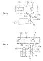
- Fig. 1 is a front view showing a semi-finished terminal supported between a pair of carriers in a method according to a first embodiment of the present invention.
- Fig. 2 is a front view showing how the semi-finished terminal illustrated in Fig. 1 appears after it has been deformed into a terminal shape.
- Fig. 3A is an enlarged view of part of Fig. 1.
- Fig. 3B is an enlarged view of part of Fig. 2.
- Fig. 4 is a side view of the terminal of Fig. 2.
- Fig. 5 is a perspective view of the terminal.
- Fig. 6 is a sectional view illustrating how a terminal produced by the first embodiment can be used.
- Fig. 7 is another sectional view illustrating how a terminal produced by the first embodiment can be used.
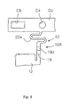
- Fig. 8 is a front view of a deformable element used in a second embodiment of the invention.
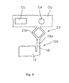
- Fig. 9 is a front view of a deformable element used in a third embodiment of the invention.
- FIG. 1 A first embodiment of the present invention will be described below with reference to Figs. 1 to 7.
- the embodiment is described in relation to the production of an electric terminal, but all features of the embodiment are applicable to the production of a different product.
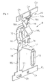
- a terminal 10 produced by the first embodiment is suitable for installation within a bulb socket B.
- the terminal 10 comprises upper and lower elastically deformable contact elements 16U and 16L, which in use are brought into contact with a contact element of a bulb (not shown), and a tab 13 to be connected with the terminal of a mating connector (not shown).
- the terminal 10 is installed in the bulb socket B by inserting it downwardly into the bulb socket, and a removal preventing element 14 of the terminal is engaged by a removal preventing element Ba of the bulb socket.
- the upper and low elastic contact elements 16U and 16L are positioned inside a bulb-installing chamber Bb open towards the upper surface of the bulb socket B, and the tab 13 is positioned inside a fit-in chamber Bc open towards the lower surface of the bulb socket B.
- a tapered portion 15 of the terminal 10 can be positioned on the tapered surface Bd such that the tapered portion 15 is in close contact with the tapered surface Bd.
- the portion of the socket a little upward from the tapered surface Bd is formed with a wide portion Be, and in use an upper base portion 12 of the terminal 10 is positioned in close contact with the wide portion Be.
- Fig. 1 shows a semi-finished terminal 10A
- Fig. 2 shows how the semi-finished terminal illustrated in Fig. 1 appears after it has been subjected to bending processing to transform it into the predetermined terminal shape.
- the semi-finished terminal 10A and the carriers CU and CL are substantially in one plane.
- the semi-finished terminal 10A is shaped into a predetermined shape by press working, cutting, and bending.
- the semi-finished terminal 10A is cut off the carriers CU and CL to form the terminal 10.
- the semi-finished terminal 10A comprises a lower base portion 11 kept flush with the lower carrier CL in the manufacturing process, an upper base portion 12 continuous with the lower base portion 11 and positioned upward (as viewed in Fig.1) from the lower base portion 11, and a tab 13 extending downward from the lower end of the lower base portion 11.
- the removal preventing element 14 is bent backwardly (i.e. in the direction into the page of Fig. 2) from the lower base portion 11 by cutting and bending a portion thereof.
- the upper base portion 12 is so shaped that it inclines backwardly from the lower base portion 11.
- a tapered portion 15 is interposed between the lower base portion 11 and the upper base portion 12.
- a curved upper elastic contact element 16U is formed by cutting and bending a portion of the upper base portion 12 frontwardly and folding a portion of the upper base portion 12 upward. A portion of the upper base portion 12 and a portion of the tapered portion 15 are cut and bent downward and frontwardly to form the lower elastic contact element 16L.
- a leg portion 17 extends downward toward the right front side continuously from the lower end of the lower base portion 11.
- a portion extending downward from the lower end of the leg portion 17 is formed into a tab 13 by folding its right and left edges forward (i.e. out of the plane of Fig. 2).
- the means for manufacturing the terminal 10 will be described below.
- a large number of semi-finished terminals 10A integral with (e.g. formed as a one-piece unit with) the pair of upper and lower carriers CU and CL, are produced in a predetermined shape by punching a sheet of metal material. All the semi-finished terminals 10A are flush with one another over their surface. Then, the semi-finished terminals 10A are sequentially supplied to processing machines, such as a pressing machine (not shown), using pilot holes Ca and Cb formed on the upper and lower carriers CU and CL. The processing machines process the semi-finished terminals into a predetermined shape by pressing, cutting, and bending. After the semi-finished terminal 10A has been processed into the predetermined shape, it is referred to herein by the reference numeral 10.
- each terminal 10 is cut at cut-off positions 18 located at the upper end of the upper base portion 12 and at the lower end of the lower base portion 11 by a cutting mechanism (not shown), to separate the terminal 10 from the pair of upper and lower carriers CU and CL. In this manner, a finished terminal 10 is obtained as a separate product.
- the upper carrier CU is integral with (e.g. a one piece unit with) the upper end of an upper supporting portion 19U extending upward (as viewed on Fig. 1) from the uppermost right end of the upper base portion 12 of the semi-finished terminal 10A
- the lower carrier CL is integral with (e.g. a one-piece unit with) the lower end of a lower supporting portion 19L extending downward from the left end of the lower base portion 11.
- a deformable portion 20 is formed at the upper end of the upper supporting portion 19U.
- a pair of narrow branch portions 20a of the deformable portion 20 extend parallel to the upper carrier CU from the upper supporting portion 19U to the right and left sides, and both ends of both branch portions 20a are connected with the upper carrier CU.
- the deformable element 20 is deformed from the state shown in Fig. 3A (in which it is parallel with the upper carrier CU), to the state shown in Fig. 3B (in which it is oblique to the upper carrier CU).
- the upper supporting portion 19U is displaced in a direction away from the upper carrier CU (i.e. downwardly on Fig. 1), without the upper supporting portion 19U being subjected to a concentration of stress and without it transmitting excess stress to the rest of the semi-finished terminal.
- a motion-resisting element 21 is formed at the lower end of the lower supporting portion 19L.
- the motion-resisting element 21 extends to the right and left sides from the lower end of the lower supporting portion 19L and is rectangular and plate-shaped.
- the motion-resisting element 21 is not deformed.
- the lower supporting portion 19L is prevented from moving away from the lower carrier CL, i.e upwardly on Fig. 1.
- a rectangular pilot hole Cb for feeding the semi-finished terminal 10A to an automatic machine is formed proximate the motion-resisting element 21. Because the motion-resisting element 21 (which is integral with the lower carrier CL) is not line-shaped but plate-shaped, it is not deformed.
- the lower carrier CL, the lower supporting portion 19L, and the lower base portion 11 are flush with one another from the start of the processing to its completion.
- the upper supporting portion 19U is bent in press working when the upper base portion 12 is displaced backwardly relatively to the lower base portion 11.
- the upper part of the upper supporting portion 19U is flush with the upper carrier CU as well as with the deformable element 20, whereas the lower part of the upper supporting portion 19U is flush with the upper base portion 12 and is displaced backwardly.
- the semi-finished terminal 10A may be twisted due to a non-uniform stress distribution in the semi-finished terminal 10A.
- the deformable element 20 is formed on the upper supporting portion 19U, the upper part of the semi-finished terminal 10A is displaced in the direction away from the upper carrier CU, with the deformable element 20 being deformed. Consequently, the tensile force acting on the semi-finished terminal 10A is relieved. Accordingly, undesirable elongation of the region of the semi-finished terminal 10A between the portion of the semi-finished terminal which is processed and the upper carrier CU, can be avoided. Thus, the semi-finished terminal 10A can be prevented from being twisted.
- the semi-finished terminal 10A can be held in a stable posture, compared with the prior art arrangement in which the semi-finished terminal is only supported by either an upper carrier or a lower carrier.
- the semi-finished terminal 10A can be processed with high accuracy.
- the semi-finished terminal 10A remains at a constant position relative to the lower carrier CL. Accordingly, when the semi-finished terminal 10A is supplied to a processing machine using the pilot holes Ca and Cb, the semi-finished terminal 10A can be placed accurately in position, and thus processing can be accomplished with high precision.
- the deformable element 22 has a construction different from that of the first embodiment.
- the other constituent parts of the second embodiment are similar to those of the first embodiment.
- the same elements are denoted by the same reference numerals, and their operation and effect are not described below.
- the deformable element 22 of the second embodiment is constituted of a narrow zigzag portion 22a connected at its respective ends to the upper end of the upper supporting portion 19U and to the upper carrier CU. Deformation of the zigzag portion 22a allows the semi-finished terminal 10A to move away from the upper carrier CU.
- the deformable element 23 has a construction different from that of the first and second embodiments.
- Other constituent parts of the third embodiment are similar to those of the first embodiment, and are denoted by the same reference numerals.
- the deformable element 23 of the third embodiment is constituted of a rhombic element 23a connected with the upper end of the upper supporting portion 19U and the upper carrier CU. Deformation of the rhombic element 23a allows the semi-finished terminal 10A to move away from the upper carrier CU.
Landscapes
- Engineering & Computer Science (AREA)
- Manufacturing & Machinery (AREA)
- Manufacturing Of Electrical Connectors (AREA)
Applications Claiming Priority (2)
| Application Number | Priority Date | Filing Date | Title |
|---|---|---|---|
| JP16728998A JP3440828B2 (ja) | 1998-06-15 | 1998-06-15 | 端子金具の製造方法 |
| JP16728998 | 1998-06-15 |
Publications (3)
| Publication Number | Publication Date |
|---|---|
| EP0966074A2 true EP0966074A2 (de) | 1999-12-22 |
| EP0966074A3 EP0966074A3 (de) | 2000-08-16 |
| EP0966074B1 EP0966074B1 (de) | 2005-03-23 |
Family
ID=15847005
Family Applications (1)
| Application Number | Title | Priority Date | Filing Date |
|---|---|---|---|
| EP99304576A Expired - Lifetime EP0966074B1 (de) | 1998-06-15 | 1999-06-11 | Herstellungsverfahren für ein Produkt und ein Zwischenprodukt |
Country Status (5)
| Country | Link |
|---|---|
| US (1) | US6141872A (de) |
| EP (1) | EP0966074B1 (de) |
| JP (1) | JP3440828B2 (de) |
| CN (1) | CN1086851C (de) |
| DE (1) | DE69924320T2 (de) |
Cited By (3)
| Publication number | Priority date | Publication date | Assignee | Title |
|---|---|---|---|---|
| EP1703600A1 (de) * | 2005-03-17 | 2006-09-20 | Sumitomo Wiring Systems, Ltd. | Kontakte in Streifen und Verfahren zur Herstellung |
| EP2461432A4 (de) * | 2009-07-31 | 2013-05-22 | Yazaki Corp | Kettenendstück |
| EP3142199B1 (de) * | 2015-09-10 | 2020-04-15 | TE Connectivity Germany GmbH | Blechmetallteil mit verbesserter verbindungslaschengeometrie und herestellungsverfharen dafür |
Families Citing this family (4)
| Publication number | Priority date | Publication date | Assignee | Title |
|---|---|---|---|---|
| DE202006017967U1 (de) * | 2006-11-23 | 2008-02-14 | Systeme + Steuerungen GmbH Elektronik und Anlagenbau für Stanz- und Umformtechnik | Einrichtung zum Positionieren eines Bauteils in einem Werkzeug einer Stanz- oder Pressvorrichtung |
| JP5805983B2 (ja) | 2011-04-21 | 2015-11-10 | 矢崎総業株式会社 | 板金部材、バスバ及びこのバスバを備えた電気接続箱 |
| JP5754501B2 (ja) * | 2013-12-26 | 2015-07-29 | 第一精工株式会社 | 中継コネクタ用端子製造方法 |
| TWI619320B (zh) * | 2016-04-01 | 2018-03-21 | 慶良電子股份有限公司 | 埋射嵌件成形方法與其所形成的前置結構、及定位邊料 |
Family Cites Families (10)
| Publication number | Priority date | Publication date | Assignee | Title |
|---|---|---|---|---|
| US3963822A (en) * | 1969-09-12 | 1976-06-15 | Noma Lites Canada Limited | Method of molding electrical lamp sockets |
| US4037915A (en) * | 1976-04-29 | 1977-07-26 | Comatel - Comptoir Europeen De Materiel Electronique | Electrical connector strips |
| US4199209A (en) * | 1978-08-18 | 1980-04-22 | Amp Incorporated | Electrical interconnecting device |
| US4783906A (en) * | 1985-11-12 | 1988-11-15 | Amp Incorporated | Method of making a customizable electrical article |
| JPS6182694A (ja) * | 1984-09-29 | 1986-04-26 | 星電器製造株式会社 | ジヤツクの製造方法 |
| JPH0622111B2 (ja) * | 1989-08-29 | 1994-03-23 | スタンレー電気株式会社 | 基板装着用電球及びその製造方法 |
| EP0444223A1 (de) * | 1990-02-27 | 1991-09-04 | INOVAN GmbH & Co. KG Metalle und Bauelemente | Kontaktfedersatz |
| JPH04366578A (ja) * | 1991-06-14 | 1992-12-18 | Nec Tohoku Ltd | コネクタ端子の製造方法 |
| DE4201670A1 (de) * | 1992-01-22 | 1993-07-29 | Amp Inc | Elektrischer kontakt sowie material und verfahren zu dessen herstellung |
| US5324215A (en) * | 1993-04-19 | 1994-06-28 | Burndy Corporation | Dual beam electrical contact |
-
1998
- 1998-06-15 JP JP16728998A patent/JP3440828B2/ja not_active Expired - Lifetime
-
1999
- 1999-06-10 US US09/329,310 patent/US6141872A/en not_active Expired - Lifetime
- 1999-06-11 DE DE69924320T patent/DE69924320T2/de not_active Expired - Lifetime
- 1999-06-11 EP EP99304576A patent/EP0966074B1/de not_active Expired - Lifetime
- 1999-06-15 CN CN99108476A patent/CN1086851C/zh not_active Expired - Lifetime
Cited By (4)
| Publication number | Priority date | Publication date | Assignee | Title |
|---|---|---|---|---|
| EP1703600A1 (de) * | 2005-03-17 | 2006-09-20 | Sumitomo Wiring Systems, Ltd. | Kontakte in Streifen und Verfahren zur Herstellung |
| EP2461432A4 (de) * | 2009-07-31 | 2013-05-22 | Yazaki Corp | Kettenendstück |
| US9419400B2 (en) | 2009-07-31 | 2016-08-16 | Yazaki Corporation | Method of manufacturing a chained terminal |
| EP3142199B1 (de) * | 2015-09-10 | 2020-04-15 | TE Connectivity Germany GmbH | Blechmetallteil mit verbesserter verbindungslaschengeometrie und herestellungsverfharen dafür |
Also Published As
| Publication number | Publication date |
|---|---|
| CN1086851C (zh) | 2002-06-26 |
| JP3440828B2 (ja) | 2003-08-25 |
| JP2000003773A (ja) | 2000-01-07 |
| US6141872A (en) | 2000-11-07 |
| EP0966074A3 (de) | 2000-08-16 |
| CN1239341A (zh) | 1999-12-22 |
| EP0966074B1 (de) | 2005-03-23 |
| DE69924320D1 (de) | 2005-04-28 |
| DE69924320T2 (de) | 2006-03-23 |
Similar Documents
| Publication | Publication Date | Title |
|---|---|---|
| US4712299A (en) | Process for producing electrical contacts for facilitating mass mounting to a contact holder | |
| US4245876A (en) | Laminated connector | |
| CN1095216C (zh) | 具有不同长度的引线的电连接器和制造该引线的方法 | |
| US4028794A (en) | Laminated connector | |
| EP0703117B1 (de) | Elektrischer Verbindungskasten | |
| US10476177B2 (en) | Electric wire with terminal and terminal crimping apparatus | |
| EP0966074B1 (de) | Herstellungsverfahren für ein Produkt und ein Zwischenprodukt | |
| US3990864A (en) | Method of making electrical contacts | |
| EP0083940B1 (de) | Bänder mit massiven elektrischen Kontakten | |
| US10290965B1 (en) | Self-gapping electrical-terminal | |
| CN107069372A (zh) | 端子压接装置 | |
| US4040177A (en) | Method of manufacturing an electrical contact | |
| US3531861A (en) | Switch contact and method of manufacture | |
| US4932903A (en) | Elastically deformable electric contact elements for incorporation in connectors and methods of manufacturing said contact elements | |
| US6793519B2 (en) | Electrical connector and method of connecting lead lines therefor | |
| US4825541A (en) | Method of making contact springs | |
| US4712850A (en) | Terminal strip with attached support and method of manufacture | |
| EP0333395A2 (de) | Elektrische Steckverbinder | |
| US4242535A (en) | Connection of wires to components having two prongs | |
| US5470261A (en) | Press-in spring contact connector | |
| JPH0745352A (ja) | 異種端子付テープおよび端子圧着機 | |
| US4626061A (en) | Crimp connect terminals | |
| US5778527A (en) | Apparatus and method for forming "L"-shaped terminals from structures stamped in a flat strip and for inserting such terminals into an electronic package | |
| JP2002292440A (ja) | クランプバネの製造方法 | |
| KR20000010925A (ko) | 히트싱크 제조 장치 및 방법 |
Legal Events
| Date | Code | Title | Description |
|---|---|---|---|
| PUAI | Public reference made under article 153(3) epc to a published international application that has entered the european phase |
Free format text: ORIGINAL CODE: 0009012 |
|
| 17P | Request for examination filed |
Effective date: 19990630 |
|
| AK | Designated contracting states |
Kind code of ref document: A2 Designated state(s): DE FR GB IT |
|
| AX | Request for extension of the european patent |
Free format text: AL;LT;LV;MK;RO;SI |
|
| PUAL | Search report despatched |
Free format text: ORIGINAL CODE: 0009013 |
|
| AK | Designated contracting states |
Kind code of ref document: A3 Designated state(s): AT BE CH CY DE DK ES FI FR GB GR IE IT LI LU MC NL PT SE |
|
| AX | Request for extension of the european patent |
Free format text: AL;LT;LV;MK;RO;SI |
|
| AKX | Designation fees paid |
Free format text: DE FR GB IT |
|
| GRAP | Despatch of communication of intention to grant a patent |
Free format text: ORIGINAL CODE: EPIDOSNIGR1 |
|
| RTI1 | Title (correction) |
Free format text: A METHOD OF MANUFACTURING A PRODUCT AND AN INTERMEDIATE PRODUCT |
|
| GRAS | Grant fee paid |
Free format text: ORIGINAL CODE: EPIDOSNIGR3 |
|
| GRAA | (expected) grant |
Free format text: ORIGINAL CODE: 0009210 |
|
| AK | Designated contracting states |
Kind code of ref document: B1 Designated state(s): DE FR GB IT |
|
| PG25 | Lapsed in a contracting state [announced via postgrant information from national office to epo] |
Ref country code: IT Free format text: LAPSE BECAUSE OF FAILURE TO SUBMIT A TRANSLATION OF THE DESCRIPTION OR TO PAY THE FEE WITHIN THE PRESCRIBED TIME-LIMIT;WARNING: LAPSES OF ITALIAN PATENTS WITH EFFECTIVE DATE BEFORE 2007 MAY HAVE OCCURRED AT ANY TIME BEFORE 2007. THE CORRECT EFFECTIVE DATE MAY BE DIFFERENT FROM THE ONE RECORDED. Effective date: 20050323 |
|
| REG | Reference to a national code |
Ref country code: GB Ref legal event code: FG4D |
|
| REF | Corresponds to: |
Ref document number: 69924320 Country of ref document: DE Date of ref document: 20050428 Kind code of ref document: P |
|
| PG25 | Lapsed in a contracting state [announced via postgrant information from national office to epo] |
Ref country code: GB Free format text: LAPSE BECAUSE OF NON-PAYMENT OF DUE FEES Effective date: 20050623 |
|
| PLBE | No opposition filed within time limit |
Free format text: ORIGINAL CODE: 0009261 |
|
| STAA | Information on the status of an ep patent application or granted ep patent |
Free format text: STATUS: NO OPPOSITION FILED WITHIN TIME LIMIT |
|
| GBPC | Gb: european patent ceased through non-payment of renewal fee |
Effective date: 20050623 |
|
| 26N | No opposition filed |
Effective date: 20051227 |
|
| EN | Fr: translation not filed | ||
| PG25 | Lapsed in a contracting state [announced via postgrant information from national office to epo] |
Ref country code: FR Free format text: LAPSE BECAUSE OF NON-PAYMENT OF DUE FEES Effective date: 20050630 |
|
| PG25 | Lapsed in a contracting state [announced via postgrant information from national office to epo] |
Ref country code: FR Free format text: LAPSE BECAUSE OF NON-PAYMENT OF DUE FEES Effective date: 20050323 |
|
| REG | Reference to a national code |
Ref country code: DE Ref legal event code: R084 Ref document number: 69924320 Country of ref document: DE |
|
| PGFP | Annual fee paid to national office [announced via postgrant information from national office to epo] |
Ref country code: DE Payment date: 20180530 Year of fee payment: 20 |
|
| REG | Reference to a national code |
Ref country code: DE Ref legal event code: R071 Ref document number: 69924320 Country of ref document: DE |