EP0967649A2 - Palladium Oberflächenschichten geeignet zum Drahtbonden und Verfahren zum Herstellen der Palladium Oberflächenschichten - Google Patents
Palladium Oberflächenschichten geeignet zum Drahtbonden und Verfahren zum Herstellen der Palladium Oberflächenschichten Download PDFInfo
- Publication number
- EP0967649A2 EP0967649A2 EP99304107A EP99304107A EP0967649A2 EP 0967649 A2 EP0967649 A2 EP 0967649A2 EP 99304107 A EP99304107 A EP 99304107A EP 99304107 A EP99304107 A EP 99304107A EP 0967649 A2 EP0967649 A2 EP 0967649A2
- Authority
- EP
- European Patent Office
- Prior art keywords
- palladium
- layer
- substrate
- nickel
- bath
- Prior art date
- Legal status (The legal status is an assumption and is not a legal conclusion. Google has not performed a legal analysis and makes no representation as to the accuracy of the status listed.)
- Ceased
Links
Images


Classifications
-
- C—CHEMISTRY; METALLURGY
- C25—ELECTROLYTIC OR ELECTROPHORETIC PROCESSES; APPARATUS THEREFOR
- C25D—PROCESSES FOR THE ELECTROLYTIC OR ELECTROPHORETIC PRODUCTION OF COATINGS; ELECTROFORMING; APPARATUS THEREFOR
- C25D3/00—Electroplating: Baths therefor
- C25D3/02—Electroplating: Baths therefor from solutions
- C25D3/50—Electroplating: Baths therefor from solutions of platinum group metals
- C25D3/52—Electroplating: Baths therefor from solutions of platinum group metals characterised by the organic bath constituents used
-
- C—CHEMISTRY; METALLURGY
- C23—COATING METALLIC MATERIAL; COATING MATERIAL WITH METALLIC MATERIAL; CHEMICAL SURFACE TREATMENT; DIFFUSION TREATMENT OF METALLIC MATERIAL; COATING BY VACUUM EVAPORATION, BY SPUTTERING, BY ION IMPLANTATION OR BY CHEMICAL VAPOUR DEPOSITION, IN GENERAL; INHIBITING CORROSION OF METALLIC MATERIAL OR INCRUSTATION IN GENERAL
- C23C—COATING METALLIC MATERIAL; COATING MATERIAL WITH METALLIC MATERIAL; SURFACE TREATMENT OF METALLIC MATERIAL BY DIFFUSION INTO THE SURFACE, BY CHEMICAL CONVERSION OR SUBSTITUTION; COATING BY VACUUM EVAPORATION, BY SPUTTERING, BY ION IMPLANTATION OR BY CHEMICAL VAPOUR DEPOSITION, IN GENERAL
- C23C28/00—Coating for obtaining at least two superposed coatings either by methods not provided for in a single one of groups C23C2/00 - C23C26/00 or by combinations of methods provided for in subclasses C23C and C25C or C25D
- C23C28/02—Coating for obtaining at least two superposed coatings either by methods not provided for in a single one of groups C23C2/00 - C23C26/00 or by combinations of methods provided for in subclasses C23C and C25C or C25D only coatings only including layers of metallic material
- C23C28/023—Coating for obtaining at least two superposed coatings either by methods not provided for in a single one of groups C23C2/00 - C23C26/00 or by combinations of methods provided for in subclasses C23C and C25C or C25D only coatings only including layers of metallic material only coatings of metal elements only
-
- C—CHEMISTRY; METALLURGY
- C25—ELECTROLYTIC OR ELECTROPHORETIC PROCESSES; APPARATUS THEREFOR
- C25D—PROCESSES FOR THE ELECTROLYTIC OR ELECTROPHORETIC PRODUCTION OF COATINGS; ELECTROFORMING; APPARATUS THEREFOR
- C25D3/00—Electroplating: Baths therefor
- C25D3/02—Electroplating: Baths therefor from solutions
- C25D3/50—Electroplating: Baths therefor from solutions of platinum group metals
-
- C—CHEMISTRY; METALLURGY
- C25—ELECTROLYTIC OR ELECTROPHORETIC PROCESSES; APPARATUS THEREFOR
- C25D—PROCESSES FOR THE ELECTROLYTIC OR ELECTROPHORETIC PRODUCTION OF COATINGS; ELECTROFORMING; APPARATUS THEREFOR
- C25D5/00—Electroplating characterised by the process; Pretreatment or after-treatment of workpieces
- C25D5/10—Electroplating with more than one layer of the same or of different metals
- C25D5/12—Electroplating with more than one layer of the same or of different metals at least one layer being of nickel or chromium
-
- H—ELECTRICITY
- H10—SEMICONDUCTOR DEVICES; ELECTRIC SOLID-STATE DEVICES NOT OTHERWISE PROVIDED FOR
- H10W—GENERIC PACKAGES, INTERCONNECTIONS, CONNECTORS OR OTHER CONSTRUCTIONAL DETAILS OF DEVICES COVERED BY CLASS H10
- H10W70/00—Package substrates; Interposers; Redistribution layers [RDL]
- H10W70/01—Manufacture or treatment
- H10W70/04—Manufacture or treatment of leadframes
-
- H—ELECTRICITY
- H10—SEMICONDUCTOR DEVICES; ELECTRIC SOLID-STATE DEVICES NOT OTHERWISE PROVIDED FOR
- H10W—GENERIC PACKAGES, INTERCONNECTIONS, CONNECTORS OR OTHER CONSTRUCTIONAL DETAILS OF DEVICES COVERED BY CLASS H10
- H10W70/00—Package substrates; Interposers; Redistribution layers [RDL]
- H10W70/40—Leadframes
- H10W70/451—Multilayered leadframes
-
- H—ELECTRICITY
- H10—SEMICONDUCTOR DEVICES; ELECTRIC SOLID-STATE DEVICES NOT OTHERWISE PROVIDED FOR
- H10W—GENERIC PACKAGES, INTERCONNECTIONS, CONNECTORS OR OTHER CONSTRUCTIONAL DETAILS OF DEVICES COVERED BY CLASS H10
- H10W70/00—Package substrates; Interposers; Redistribution layers [RDL]
- H10W70/40—Leadframes
- H10W70/456—Materials
- H10W70/457—Materials of metallic layers on leadframes
-
- H—ELECTRICITY
- H10—SEMICONDUCTOR DEVICES; ELECTRIC SOLID-STATE DEVICES NOT OTHERWISE PROVIDED FOR
- H10W—GENERIC PACKAGES, INTERCONNECTIONS, CONNECTORS OR OTHER CONSTRUCTIONAL DETAILS OF DEVICES COVERED BY CLASS H10
- H10W72/00—Interconnections or connectors in packages
- H10W72/071—Connecting or disconnecting
- H10W72/0711—Apparatus therefor
- H10W72/07141—Means for applying energy, e.g. ovens or lasers
-
- H—ELECTRICITY
- H10—SEMICONDUCTOR DEVICES; ELECTRIC SOLID-STATE DEVICES NOT OTHERWISE PROVIDED FOR
- H10W—GENERIC PACKAGES, INTERCONNECTIONS, CONNECTORS OR OTHER CONSTRUCTIONAL DETAILS OF DEVICES COVERED BY CLASS H10
- H10W72/00—Interconnections or connectors in packages
- H10W72/071—Connecting or disconnecting
- H10W72/075—Connecting or disconnecting of bond wires
- H10W72/07521—Aligning
-
- H—ELECTRICITY
- H10—SEMICONDUCTOR DEVICES; ELECTRIC SOLID-STATE DEVICES NOT OTHERWISE PROVIDED FOR
- H10W—GENERIC PACKAGES, INTERCONNECTIONS, CONNECTORS OR OTHER CONSTRUCTIONAL DETAILS OF DEVICES COVERED BY CLASS H10
- H10W72/00—Interconnections or connectors in packages
- H10W72/071—Connecting or disconnecting
- H10W72/075—Connecting or disconnecting of bond wires
- H10W72/07531—Techniques
- H10W72/07532—Compression bonding, e.g. thermocompression bonding
- H10W72/07533—Ultrasonic bonding, e.g. thermosonic bonding
-
- H—ELECTRICITY
- H10—SEMICONDUCTOR DEVICES; ELECTRIC SOLID-STATE DEVICES NOT OTHERWISE PROVIDED FOR
- H10W—GENERIC PACKAGES, INTERCONNECTIONS, CONNECTORS OR OTHER CONSTRUCTIONAL DETAILS OF DEVICES COVERED BY CLASS H10
- H10W72/00—Interconnections or connectors in packages
- H10W72/50—Bond wires
- H10W72/531—Shapes of wire connectors
- H10W72/536—Shapes of wire connectors the connected ends being ball-shaped
-
- H—ELECTRICITY
- H10—SEMICONDUCTOR DEVICES; ELECTRIC SOLID-STATE DEVICES NOT OTHERWISE PROVIDED FOR
- H10W—GENERIC PACKAGES, INTERCONNECTIONS, CONNECTORS OR OTHER CONSTRUCTIONAL DETAILS OF DEVICES COVERED BY CLASS H10
- H10W72/00—Interconnections or connectors in packages
- H10W72/50—Bond wires
- H10W72/531—Shapes of wire connectors
- H10W72/5363—Shapes of wire connectors the connected ends being wedge-shaped
-
- H—ELECTRICITY
- H10—SEMICONDUCTOR DEVICES; ELECTRIC SOLID-STATE DEVICES NOT OTHERWISE PROVIDED FOR
- H10W—GENERIC PACKAGES, INTERCONNECTIONS, CONNECTORS OR OTHER CONSTRUCTIONAL DETAILS OF DEVICES COVERED BY CLASS H10
- H10W72/00—Interconnections or connectors in packages
- H10W72/50—Bond wires
- H10W72/541—Dispositions of bond wires
- H10W72/5449—Dispositions of bond wires not being orthogonal to a side surface of the chip, e.g. fan-out arrangements
-
- H—ELECTRICITY
- H10—SEMICONDUCTOR DEVICES; ELECTRIC SOLID-STATE DEVICES NOT OTHERWISE PROVIDED FOR
- H10W—GENERIC PACKAGES, INTERCONNECTIONS, CONNECTORS OR OTHER CONSTRUCTIONAL DETAILS OF DEVICES COVERED BY CLASS H10
- H10W72/00—Interconnections or connectors in packages
- H10W72/50—Bond wires
- H10W72/551—Materials of bond wires
- H10W72/552—Materials of bond wires comprising metals or metalloids, e.g. silver
- H10W72/5522—Materials of bond wires comprising metals or metalloids, e.g. silver comprising gold [Au]
-
- H—ELECTRICITY
- H10—SEMICONDUCTOR DEVICES; ELECTRIC SOLID-STATE DEVICES NOT OTHERWISE PROVIDED FOR
- H10W—GENERIC PACKAGES, INTERCONNECTIONS, CONNECTORS OR OTHER CONSTRUCTIONAL DETAILS OF DEVICES COVERED BY CLASS H10
- H10W72/00—Interconnections or connectors in packages
- H10W72/50—Bond wires
- H10W72/551—Materials of bond wires
- H10W72/552—Materials of bond wires comprising metals or metalloids, e.g. silver
- H10W72/5524—Materials of bond wires comprising metals or metalloids, e.g. silver comprising aluminium [Al]
-
- H—ELECTRICITY
- H10—SEMICONDUCTOR DEVICES; ELECTRIC SOLID-STATE DEVICES NOT OTHERWISE PROVIDED FOR
- H10W—GENERIC PACKAGES, INTERCONNECTIONS, CONNECTORS OR OTHER CONSTRUCTIONAL DETAILS OF DEVICES COVERED BY CLASS H10
- H10W72/00—Interconnections or connectors in packages
- H10W72/50—Bond wires
- H10W72/59—Bond pads specially adapted therefor
-
- H—ELECTRICITY
- H10—SEMICONDUCTOR DEVICES; ELECTRIC SOLID-STATE DEVICES NOT OTHERWISE PROVIDED FOR
- H10W—GENERIC PACKAGES, INTERCONNECTIONS, CONNECTORS OR OTHER CONSTRUCTIONAL DETAILS OF DEVICES COVERED BY CLASS H10
- H10W72/00—Interconnections or connectors in packages
- H10W72/90—Bond pads, in general
- H10W72/951—Materials of bond pads
- H10W72/952—Materials of bond pads comprising metals or metalloids, e.g. PbSn, Ag or Cu
-
- H—ELECTRICITY
- H10—SEMICONDUCTOR DEVICES; ELECTRIC SOLID-STATE DEVICES NOT OTHERWISE PROVIDED FOR
- H10W—GENERIC PACKAGES, INTERCONNECTIONS, CONNECTORS OR OTHER CONSTRUCTIONAL DETAILS OF DEVICES COVERED BY CLASS H10
- H10W90/00—Package configurations
- H10W90/701—Package configurations characterised by the relative positions of pads or connectors relative to package parts
- H10W90/751—Package configurations characterised by the relative positions of pads or connectors relative to package parts of bond wires
- H10W90/756—Package configurations characterised by the relative positions of pads or connectors relative to package parts of bond wires between a chip and a stacked lead frame, conducting package substrate or heat sink
-
- Y—GENERAL TAGGING OF NEW TECHNOLOGICAL DEVELOPMENTS; GENERAL TAGGING OF CROSS-SECTIONAL TECHNOLOGIES SPANNING OVER SEVERAL SECTIONS OF THE IPC; TECHNICAL SUBJECTS COVERED BY FORMER USPC CROSS-REFERENCE ART COLLECTIONS [XRACs] AND DIGESTS
- Y10—TECHNICAL SUBJECTS COVERED BY FORMER USPC
- Y10S—TECHNICAL SUBJECTS COVERED BY FORMER USPC CROSS-REFERENCE ART COLLECTIONS [XRACs] AND DIGESTS
- Y10S428/00—Stock material or miscellaneous articles
- Y10S428/922—Static electricity metal bleed-off metallic stock
- Y10S428/923—Physical dimension
- Y10S428/924—Composite
- Y10S428/926—Thickness of individual layer specified
-
- Y—GENERAL TAGGING OF NEW TECHNOLOGICAL DEVELOPMENTS; GENERAL TAGGING OF CROSS-SECTIONAL TECHNOLOGIES SPANNING OVER SEVERAL SECTIONS OF THE IPC; TECHNICAL SUBJECTS COVERED BY FORMER USPC CROSS-REFERENCE ART COLLECTIONS [XRACs] AND DIGESTS
- Y10—TECHNICAL SUBJECTS COVERED BY FORMER USPC
- Y10S—TECHNICAL SUBJECTS COVERED BY FORMER USPC CROSS-REFERENCE ART COLLECTIONS [XRACs] AND DIGESTS
- Y10S428/00—Stock material or miscellaneous articles
- Y10S428/922—Static electricity metal bleed-off metallic stock
- Y10S428/9335—Product by special process
- Y10S428/934—Electrical process
- Y10S428/935—Electroplating
-
- Y—GENERAL TAGGING OF NEW TECHNOLOGICAL DEVELOPMENTS; GENERAL TAGGING OF CROSS-SECTIONAL TECHNOLOGIES SPANNING OVER SEVERAL SECTIONS OF THE IPC; TECHNICAL SUBJECTS COVERED BY FORMER USPC CROSS-REFERENCE ART COLLECTIONS [XRACs] AND DIGESTS
- Y10—TECHNICAL SUBJECTS COVERED BY FORMER USPC
- Y10T—TECHNICAL SUBJECTS COVERED BY FORMER US CLASSIFICATION
- Y10T428/00—Stock material or miscellaneous articles
- Y10T428/12—All metal or with adjacent metals
- Y10T428/12493—Composite; i.e., plural, adjacent, spatially distinct metal components [e.g., layers, joint, etc.]
- Y10T428/12639—Adjacent, identical composition, components
- Y10T428/12646—Group VIII or IB metal-base
-
- Y—GENERAL TAGGING OF NEW TECHNOLOGICAL DEVELOPMENTS; GENERAL TAGGING OF CROSS-SECTIONAL TECHNOLOGIES SPANNING OVER SEVERAL SECTIONS OF THE IPC; TECHNICAL SUBJECTS COVERED BY FORMER USPC CROSS-REFERENCE ART COLLECTIONS [XRACs] AND DIGESTS
- Y10—TECHNICAL SUBJECTS COVERED BY FORMER USPC
- Y10T—TECHNICAL SUBJECTS COVERED BY FORMER US CLASSIFICATION
- Y10T428/00—Stock material or miscellaneous articles
- Y10T428/12—All metal or with adjacent metals
- Y10T428/12493—Composite; i.e., plural, adjacent, spatially distinct metal components [e.g., layers, joint, etc.]
- Y10T428/12771—Transition metal-base component
- Y10T428/12861—Group VIII or IB metal-base component
- Y10T428/12875—Platinum group metal-base component
-
- Y—GENERAL TAGGING OF NEW TECHNOLOGICAL DEVELOPMENTS; GENERAL TAGGING OF CROSS-SECTIONAL TECHNOLOGIES SPANNING OVER SEVERAL SECTIONS OF THE IPC; TECHNICAL SUBJECTS COVERED BY FORMER USPC CROSS-REFERENCE ART COLLECTIONS [XRACs] AND DIGESTS
- Y10—TECHNICAL SUBJECTS COVERED BY FORMER USPC
- Y10T—TECHNICAL SUBJECTS COVERED BY FORMER US CLASSIFICATION
- Y10T428/00—Stock material or miscellaneous articles
- Y10T428/12—All metal or with adjacent metals
- Y10T428/12493—Composite; i.e., plural, adjacent, spatially distinct metal components [e.g., layers, joint, etc.]
- Y10T428/12771—Transition metal-base component
- Y10T428/12861—Group VIII or IB metal-base component
- Y10T428/12882—Cu-base component alternative to Ag-, Au-, or Ni-base component
-
- Y—GENERAL TAGGING OF NEW TECHNOLOGICAL DEVELOPMENTS; GENERAL TAGGING OF CROSS-SECTIONAL TECHNOLOGIES SPANNING OVER SEVERAL SECTIONS OF THE IPC; TECHNICAL SUBJECTS COVERED BY FORMER USPC CROSS-REFERENCE ART COLLECTIONS [XRACs] AND DIGESTS
- Y10—TECHNICAL SUBJECTS COVERED BY FORMER USPC
- Y10T—TECHNICAL SUBJECTS COVERED BY FORMER US CLASSIFICATION
- Y10T428/00—Stock material or miscellaneous articles
- Y10T428/12—All metal or with adjacent metals
- Y10T428/12493—Composite; i.e., plural, adjacent, spatially distinct metal components [e.g., layers, joint, etc.]
- Y10T428/12771—Transition metal-base component
- Y10T428/12861—Group VIII or IB metal-base component
- Y10T428/12903—Cu-base component
- Y10T428/1291—Next to Co-, Cu-, or Ni-base component
-
- Y—GENERAL TAGGING OF NEW TECHNOLOGICAL DEVELOPMENTS; GENERAL TAGGING OF CROSS-SECTIONAL TECHNOLOGIES SPANNING OVER SEVERAL SECTIONS OF THE IPC; TECHNICAL SUBJECTS COVERED BY FORMER USPC CROSS-REFERENCE ART COLLECTIONS [XRACs] AND DIGESTS
- Y10—TECHNICAL SUBJECTS COVERED BY FORMER USPC
- Y10T—TECHNICAL SUBJECTS COVERED BY FORMER US CLASSIFICATION
- Y10T428/00—Stock material or miscellaneous articles
- Y10T428/12—All metal or with adjacent metals
- Y10T428/12493—Composite; i.e., plural, adjacent, spatially distinct metal components [e.g., layers, joint, etc.]
- Y10T428/12771—Transition metal-base component
- Y10T428/12861—Group VIII or IB metal-base component
- Y10T428/12944—Ni-base component
Definitions
- the present invention relates to palladium surface coatings, and more particularly, to palladium surface coatings useful in packaging integrated circuit devices.
- Integrated circuit (IC) packages are protective enclosures within which are typically sealed an integrated circuit (IC) unit and a leadframe.
- the IC unit is attached to the leadframe.
- the leadframe electrically interconnects the IC unit to circuitry located outside of the IC package.
- FIG. 1 A leadframe 10 useful for integrated circuit packages is shown in FIG. 1.
- the leadframe 10 includes a mounting area 15 and a plurality of lead members 20 .
- the lead members 20 extend away from locations 25 adjacent to the mounting area 15 .
- An IC unit 30 is attached on the mounting area 15 of leadframe 10 .
- Examples of IC units include integrated circuit chips and hybrid integrated circuit modules.
- Hybrid integrated circuit modules typically include one or more IC chips as well as other electronic components mounted on a plastic or ceramic carrier.
- wire bonds 35 are formed between the IC unit 30 and the lead members 20 .
- the wire bonds 35 electrically connect the IC unit 30 with the lead members 20 .
- Wire bonds are typically made of gold and aluminum wires.
- thermosonic techniques a wire 50 is threaded through a capillary 55 , so an end of the wire protrudes therefrom, as shown in FIG. 2A.
- the end of the wire that protrudes from the capillary 55 is then melted by an electrical spark, forming a ball 60 just below the tip of the capillary 55 , as depicted in FIG. 2B.
- the ball 60 is formed, it is bonded to an IC unit 70 mounted on a portion of a leadframe 75 , as shown in FIG. 2C.
- the ball 60 is bonded to the IC unit 70 by applying a vertical load on the ball 60 , pressing it against the surface of the IC unit 70 while ultrasonically exciting the wire.
- the IC unit As the ball 60 is pressed against the IC unit 70 the IC unit is heated. After the ball 60 is attached to the IC unit 70 , the wire 50 is looped and a wedge bond 80 (crescent bond) is formed to the leadframe 75 , as depicted in FIG. 2D.
- the wedge bond 80 is also formed by applying a vertical load to the portion of the wire 50 in contact with the lead frame 75 , pressing it against the surface of the leadframe 75 while ultrasonically exciting the wire.
- the leadframe 75 As the wedge bond is formed the leadframe 75 is heated.
- the capillary 55 breaks the wire 50 so the wedge bond 80 covers a crescent-shaped area on the surface of the leadframe 75 , as depicted in FIG. 2E.
- Leadframes are made of a variety of materials. Suitable leadframe materials are selected for their mechanical strength, conductivity, machinability, formability, corrosion resistance, thermal expansion as well as their solderability and wirebondability. Although suitable leadframe materials include gold and palladium, the cost of these materials makes their use prohibitive for most applications.
- leadframes are made of materials such as copper and copper alloys.
- suitable copper alloys include alloy 151 (99.9 weight % copper, 0.1 weight % zirconium); alloy 194 (97.5 weight % copper, 2.35 weight % iron, 0.03 weight % phosphorous, 0.12 weight % zinc); and alloy 7025 (96.2 weight % copper, 3.0 weight % nickel, 0.65 weight % silicon, 0.15 weight % magnesium).
- reactive copper products e. g., copper oxides
- leadframes made of copper and copper alloys are coated with a layer of nickel.
- the nickel layer serves as a barrier to the formation of copper oxides on the surface of the leadframe.
- nickel also oxidizes in air, and such oxides are undesirable.
- a thin layer of a metal that does not oxidize is formed over the nickel layer to prevent oxide formation. Examples of these materials, typically referred to as “noble metals" include gold and palladium.
- Nickel coatings formed on the leadframes using conventional electrodeposition techniques have a tendency to crack when the lead members of the leadframe are bent at angles of about 82 degrees to about 90 degrees with a radius of about 250 ⁇ m for connection to larger assemblies.
- the layer of noble metal thereon also cracks exposing the underlying copper leadframe to oxygen, and potentially forming oxides thereon.
- the present invention is directed to a surface finish which provides improved wirebonding performance for integrated circuit packages.
- the surface finish which is formed on a substrate includes a palladium layer and one or more material layers.
- the one or more material layers are interposed between the substrate and the palladium layer.
- the palladium layer has a hardness that is less than about 500 (KHN 50 ) while at least one material layer has a hardness that is less than about 250 (KHN 50 ).
- KHN 50 as used in this disclosure describes the indentability of a material under a specified load.
- KHN 50 as used in this disclosure identifies the Knoop hardness number of a material under a 50 gram load.
- KHN 50 palladium layers with hardnesses less than about 500 (KHN 50 ) formed over a material layer or layers with hardnesses less than about 250 (KHN 50 ) are ductile. Such ductile layers typically do not crack during IC package assembly, preventing oxides from forming thereon. Oxide formation is undesirable because it prevents wirebonds from adhering to the surface finish.
- the substrate is made of a material useful for an integrated circuit package.
- suitable substrate materials include copper or copper alloys, and nickel or nickel alloys.
- the material layer or layers interposed between the substrate and the palladium layer are formed using any suitable method such as electroplating.
- An example of a suitable material layer includes nickel.
- the palladium layer is formed over the material layer or layers by electroplating the substrate in a palladium bath that contains about 5 gm/l to about 20 gm/l of palladium.
- the palladium bath is maintained at a pH of about 7.0 to about 8.0.
- Palladium is plated over the material layer using a current density of about 5 Amps/ft 2 to about 150 Amps/ft 2 , at a bath temperature of about 25 °C to about 65 °C.
- the palladium bath is agitated at a speed of about 10 cm/sec to about 100 cm/sec.
- the palladium bath optionally includes an additive which is useful for controlling the hardness of palladium layers plated therefrom.
- Additives useful for controlling palladium layer hardness include many sulfur-containing organic compounds. Examples of additives useful for controlling palladium layer hardness include benzenesulfonic acid and allyl phenyl sulfone.
- the palladium layer preferably has a thickness greater than about 0.075 ⁇ m. Palladium layer thicknesses greater than about 0.075 ⁇ m prevent oxides from forming on the underlying material layers.
- the present invention is directed to a surface finish which provides improved wirebonding performance for integrated circuit packages.
- the surface finish which is formed on a substrate includes a palladium layer and one or more material layers.
- the one or more material layers are interposed between the substrate and the palladium layer.
- the palladium layer has a hardness that is less than about 500 (KHN 50 ) while at least one material layer has a hardness that is less than about 250 (KHN 50 ).
- KHN 50 palladium layers with hardnesses less than about 500 (KHN 50 ) formed over a material layer or layers with hardnesses less than about 250 (KHN 50 ) are ductile. Such ductile layers typically do not crack during IC package assembly, preventing oxides from forming thereon. Oxides on the surface finish are undesirable because they prevent wirebonds from adhering to the palladium layer.
- FIG. 3 shows a cross-sectional view of a substrate 100 useful in integrated circuit packages.
- Substrate 100 has an IC mounting area 110 with a plurality of separate lead members 120 extending away from locations adjacent to the mounting area 110 .
- An IC unit 125 is attached to mounting area 110 .
- Wire bonds 135 formed between the IC unit 125 and the lead members 120 electrically connect the IC unit 125 with leadframe 100 .
- Substrate 100 is made of a material useful for an integrated circuit package.
- suitable substrate materials include copper or copper alloys, and nickel or nickel alloys.
- the material layer 155 or layers interposed between with the substrate 100 and the palladium layer 150 are formed using any suitable method such as electroplating.
- a nickel layer with a hardness less than about 250 is electroplated on the substrate from a NikelTech MLS nickel bath containing about 100 gm/l to about 130 gm/l nickel.
- the nickel bath is maintained at a pH of about 2.0 to about 2.5.
- Nickel is plated on the substrate using a current density of about 50 Amps/ft 2 to about 300 Amps/ft 2 at a bath temperature of about 50 °C to about 65 °C. It is advantageous if the bath is agitated at a speed of about 10 cm/sec to about 100 cm/sec.
- NikelTech MLS nickel baths are commercially available from Lucent Technologies Inc., Murray Hill, N.J.
- a palladium layer 150 with a hardness less than about 500 (KHN 50 ) is formed on the at least one material layer 155 .
- the palladium layer is formed on the material layer or layers by electroplating the substrate in a palladium bath that contains about 5 gm/l to about 20 gm/l of palladium.
- the palladium bath is maintained at a pH of about 7.0 to about 8.0.
- Palladium is plated on the at least one material layer using a current density of about 5 Amps/ft 2 to about 150 Amps/ft 2 , at a bath temperature of about 25 °C to about 65 °C. It is advantageous if the plating bath is agitated at a speed of about 10 cm/sec to about 100 cm/sec.
- Palladium in the aqueous bath is a soluble species suitable for use in an electroplating process.
- Particularly useful are palladium complex ion compounds including palladium tetra-amine salts such as Pd(NH 3 ) 4 Cl 2 and the corresponding bromides and iodides as well as other stable anions such as sulfates, and various palladium complexes in which the complexing agent is an organic compound such as an amine (see for example U.S. Pat. No. 4,911,799 which is hereby incorporated by reference).
- palladium complex hydroxides such as palladium hydroxide complexed with various organic compounds such as organic amines and polyamines (e.g. di- ⁇ -hydroxo-bis-[cis-diamine palladium (II)]).
- halide palladium salts including palladium halide complex salts (particularly chlorides) are preferred as are sulfate palladium salts because of stability and high solubility.
- ammonia is preferred as the complexing agent (palladium amine salts) because of cost, availability, solubility and ease of removing the ammonia from the bath.
- the palladium bath optionally includes an additive which controls the hardness of palladium layers plated therefrom.
- Additives which control the hardness of palladium layers plated from palladium baths include sulfur-containing organic compounds. Suitable examples are o-benzaldehydesulfonic acid, 1-naphthalene sulfonic acid, 2-naphthalenesulfonic acid, benzenesulfinic acid, oxy-4,4-bis(benzene)sulfinic acid, p-toluene sulfinic acid, and 3-trifluoromethyl benzene sulfinic acid.
- Additional additives include allyl phenyl sulfone, o-benzoic sulfamide, benzylsulfonyl propionamide, phenylsulfonyl acetamide, 3-(phenylsulfonyl) propionamide, benzene sulfonamide, bis (phenylsulfonyl) methane, guanidine carbonate, sulfaguanidine and nicotinic acid.
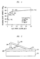
- the graph of FIG. 4 plots the hardness of electroplated palladium layers as a function of the concentration of an additive (allyl phenyl sulfone) in the palladium plating bath.
- the graph of FIG. 4 illustrates that electroplated palladium layers formed from palladium plating baths containing less than about 0.1 gm/l allyl phenyl sulfone have hardnesses ranging from about 180 (KHN 50 ) to about 460 (KHN 50 ).
- the palladium layer preferably has a thickness greater then 0.075 ⁇ m. Additionally, a gold flash layer is optionally plated over the palladium layer. The gold flash layer preferably has a thickness of about 0.005 ⁇ m to about 0.075 ⁇ m.
- the wirebondability of the palladium surface finish is evaluated by performing pull-tests on wirebonds formed thereto, as shown in FIG. 5.
- Each wirebond includes both a ball bond 220 and a wedge bond 210 which are formed to a palladium layer 200 .
- Interposed between the palladium layer 200 and a substrate 250 is a nickel layer 255 .
- a force is applied to the wirebond, by pulling on the wire 240 with a steel hook 230 .
- the force is increased until the wire 240 breaks or either of the ball 220 and wedge bond 210 lifts away from the palladium surface 200 .
- the wirebond should break along the length of the wire 240 instead of lifting away from the palladium surface 200 under either the ball bond 220 or the wedge bond 210 .
- a wirebondable surface is typically determined based on the number of bond failures resulting from nonadhesion of either the ball bonds or the wedge bonds on the palladium surface. For some applications, one bond failure identifies a palladium surface finish as a poor wirebonding surface.
- wirebonds withstand a minimum pull force.
- some industry standards require that wirebonds made using 25 ⁇ m diameter gold wire, with between about 3 % to about 6 % elongation and breaking load of about 8 grams to about 10 grams, withstand pull forces of at least about 5.00 grams.
- breaking load as used in this disclosure identifies the force above which a wire is expected to break when it is pulled laterally along its length.
- a 194 copper alloy leadframe was plated with a nickel layer.
- the 194 copper alloy leadframe was obtained from Olin Corporation, Norwalk, Conn.
- the nickel was plated from a NikelTech MLS nickel bath containing about 120 g/l nickel.
- the nickel layer was plated with a current density of about 100 Amps/ft 2 at a temperature of about 60 °C and pH of about 2.2.
- a nickel layer about 2.5 ⁇ m thick was plated on the copper alloy leadframe.
- the nickel had a hardness of about 200 KHN 50 .
- the NikelTech MLS nickel bath was obtained from Lucent Technologies, Murray Hill, N. J.
- a palladium coating was formed over the nickel layer.
- the palladium was plated from a PallaTech PdLF palladium bath containing 5 gm/l palladium and about 0.5 gm/l of allyl phenyl sulfone.
- the palladium coating was plated with a current density of 10 Amps/ft 2 at a temperature of 22 °C and pH of 7.0.
- a palladium layer about 0.175 ⁇ m was plated over the nickel layer.
- the palladium coating had a hardness of about 516 KHN 50 .
- the PallaTech PdLF palladium bath was obtained from Lucent Technologies, Murray Hill, N. J.
- the gold wire bonds were formed on the nickel/palladium coated leadframe.
- the gold wire had a diameter of 25 ⁇ m, with between 3 % to 6 % elongation, and a breaking load of about 8 grams to about 10 grams.
- the gold wire was obtained from Kulicke & Soffa Industries, Inc. (American Fine Wire, Packaging Materials Group), Selma, Alabama. Pull tests were performed to test the strength of each wire bond. One wire bond did not adhere to the palladium surface. Pull-forces as low as 2.00 grams were found to remove wire bonds formed on the palladium coated leadframe.
- a leadframe was plated with a conformable nickel layer.
- the nickel was plated according to the conditions described in Example 1.
- a palladium coating was formed over the nickel layer.
- the palladium was plated from a PallaTech PdLF palladium bath containing 10 gm/l palladium and about 0.05 gm/l of allyl phenyl sulfone.
- the palladium coating was plated with a current density of 6 Amps/ft 2 at a temperature of 35 °C and pH of 7.5.
- a palladium layer about 0.175 ⁇ m thick was plated on the nickel layer.
- the palladium coating had a hardness of about 425 KHN 50 .
- a leadframe was plated with a conformable nickel layer.
- the nickel was plated according to the conditions described in Example 1.
- a palladium coating was formed over the nickel layer.
- the palladium was plated from a PallaTech PdLF palladium bath containing 25 gm/l palladium.
- the palladium coating was plated with a current density of 10 Amps/ft 2 at a temperature of 65 °C and pH of 8.0.
- a palladium layer about 0.175 ⁇ m thick was plated on the nickel layer.
- the palladium coating had a hardness of about 145 KHN 50 .
- a leadframe was plated with nickel/palladium layers.
- the nickel and palladium layers were plated according to the conditions described in Example 2.
- a gold flash was plated over the nickel/palladium layers.
- the gold flash was plated from a AuRoTech P gold bath containing 8 gm/l gold.
- the gold flash was plated with a current density of 1 Amps/ft 2 at a temperature of 55 °C and pH of 5.5.
- a gold flash about 0.025 ⁇ m thick was plated over the nickel/palladium layers.
- the AuRoTech P gold bath was obtained from Lucent Technologies, Murray Hill, N. J.
Landscapes
- Chemical & Material Sciences (AREA)
- Organic Chemistry (AREA)
- Engineering & Computer Science (AREA)
- Chemical Kinetics & Catalysis (AREA)
- Materials Engineering (AREA)
- Metallurgy (AREA)
- Electrochemistry (AREA)
- Mechanical Engineering (AREA)
- Electroplating Methods And Accessories (AREA)
- Electroplating And Plating Baths Therefor (AREA)
- Lead Frames For Integrated Circuits (AREA)
- Parts Printed On Printed Circuit Boards (AREA)
- Chemically Coating (AREA)
- Other Surface Treatments For Metallic Materials (AREA)
Applications Claiming Priority (2)
| Application Number | Priority Date | Filing Date | Title |
|---|---|---|---|
| US95237 | 1998-06-10 | ||
| US09/095,237 US6139977A (en) | 1998-06-10 | 1998-06-10 | Palladium surface coating suitable for wirebonding and process for forming palladium surface coatings |
Publications (2)
| Publication Number | Publication Date |
|---|---|
| EP0967649A2 true EP0967649A2 (de) | 1999-12-29 |
| EP0967649A3 EP0967649A3 (de) | 2003-01-15 |
Family
ID=22250856
Family Applications (1)
| Application Number | Title | Priority Date | Filing Date |
|---|---|---|---|
| EP99304107A Ceased EP0967649A3 (de) | 1998-06-10 | 1999-05-26 | Palladium Oberflächenschichten geeignet zum Drahtbonden und Verfahren zum Herstellen der Palladium Oberflächenschichten |
Country Status (7)
| Country | Link |
|---|---|
| US (1) | US6139977A (de) |
| EP (1) | EP0967649A3 (de) |
| JP (1) | JP2000012755A (de) |
| KR (1) | KR20000006033A (de) |
| CA (1) | CA2270303A1 (de) |
| SG (1) | SG77691A1 (de) |
| TW (1) | TW480292B (de) |
Cited By (3)
| Publication number | Priority date | Publication date | Assignee | Title |
|---|---|---|---|---|
| EP1126520A3 (de) * | 2000-02-18 | 2002-11-20 | Hitachi, Ltd. | IC-Vorrichtung und Methode zur Herstellung |
| US7071571B2 (en) | 2003-07-24 | 2006-07-04 | Infineon Technoloiges Ag | Semiconductor component having a plastic housing and methods for its production |
| WO2008099326A1 (en) * | 2007-02-14 | 2008-08-21 | Nxp B.V. | A carrier for bonding a semiconductor chip onto and a method of contacting a semiconductor chip to a carrier |
Families Citing this family (12)
| Publication number | Priority date | Publication date | Assignee | Title |
|---|---|---|---|---|
| US6335107B1 (en) * | 1999-09-23 | 2002-01-01 | Lucent Technologies Inc. | Metal article coated with multilayer surface finish for porosity reduction |
| JP2001185670A (ja) * | 1999-12-10 | 2001-07-06 | Texas Instr Inc <Ti> | リードフレームとその製法 |
| US6335104B1 (en) * | 2000-02-22 | 2002-01-01 | International Business Machines Corporation | Method for preparing a conductive pad for electrical connection and conductive pad formed |
| US6478212B1 (en) | 2001-01-16 | 2002-11-12 | International Business Machines Corporation | Bond pad structure and method for reduced downward force wirebonding |
| JP2003297994A (ja) * | 2002-03-29 | 2003-10-17 | Hitachi Ltd | 半導体装置およびその製造方法 |
| US20050268991A1 (en) * | 2004-06-03 | 2005-12-08 | Enthone Inc. | Corrosion resistance enhancement of tin surfaces |
| JP5554718B2 (ja) | 2007-12-11 | 2014-07-23 | エンソン インコーポレイテッド | ナノ粒子を含む金属系複合コーティングの電解デポジット |
| TWI452640B (zh) * | 2009-02-09 | 2014-09-11 | 日月光半導體製造股份有限公司 | 半導體封裝構造及其封裝方法 |
| US8834729B2 (en) * | 2009-11-30 | 2014-09-16 | Eastman Kodak Company | Method of making bondable printed wiring member |
| US8251494B2 (en) * | 2009-11-30 | 2012-08-28 | Eastman Kodak Company | Bondable printed wiring with improved wear resistance |
| US8801914B2 (en) | 2011-05-26 | 2014-08-12 | Eastman Kodak Company | Method of making wear-resistant printed wiring member |
| JP2014207389A (ja) | 2013-04-15 | 2014-10-30 | 株式会社東芝 | 半導体パッケージ |
Family Cites Families (7)
| Publication number | Priority date | Publication date | Assignee | Title |
|---|---|---|---|---|
| US4545868A (en) * | 1981-10-06 | 1985-10-08 | Learonal, Inc. | Palladium plating |
| US4785137A (en) * | 1984-04-30 | 1988-11-15 | Allied Corporation | Novel nickel/indium/other metal alloy for use in the manufacture of electrical contact areas of electrical devices |
| US5024733A (en) * | 1989-08-29 | 1991-06-18 | At&T Bell Laboratories | Palladium alloy electroplating process |
| US4911799A (en) * | 1989-08-29 | 1990-03-27 | At&T Bell Laboratories | Electrodeposition of palladium films |
| JPH0750377A (ja) * | 1993-08-05 | 1995-02-21 | Kobe Steel Ltd | 半導体用リードフレーム |
| JPH07240488A (ja) * | 1994-02-28 | 1995-09-12 | Nec Corp | 半導体装置およびその製造方法 |
| US5675177A (en) * | 1995-06-26 | 1997-10-07 | Lucent Technologies Inc. | Ultra-thin noble metal coatings for electronic packaging |
-
1998
- 1998-06-10 US US09/095,237 patent/US6139977A/en not_active Expired - Lifetime
-
1999
- 1999-04-27 CA CA002270303A patent/CA2270303A1/en not_active Abandoned
- 1999-05-06 TW TW088107348A patent/TW480292B/zh not_active IP Right Cessation
- 1999-05-26 EP EP99304107A patent/EP0967649A3/de not_active Ceased
- 1999-06-07 SG SG1999002769A patent/SG77691A1/en unknown
- 1999-06-09 KR KR1019990021311A patent/KR20000006033A/ko not_active Ceased
- 1999-06-10 JP JP11163170A patent/JP2000012755A/ja not_active Ceased
Non-Patent Citations (1)
| Title |
|---|
| PEARLSTEIN F. AND WEIGHTMAN R.F.: "Electroless Palladium Deposition", PLATING, vol. 56, no. 10, pages 1158 - 1161, XP001153777 * |
Cited By (9)
| Publication number | Priority date | Publication date | Assignee | Title |
|---|---|---|---|---|
| EP1126520A3 (de) * | 2000-02-18 | 2002-11-20 | Hitachi, Ltd. | IC-Vorrichtung und Methode zur Herstellung |
| US6891253B2 (en) | 2000-02-18 | 2005-05-10 | Renesas Technology Corp. | Semiconductor integrated circuit device and method of manufacturing the same |
| US7038306B2 (en) | 2000-02-18 | 2006-05-02 | Hitachi, Ltd. | Semiconductor integrated circuit device and method of manufacturing the same |
| US7176056B2 (en) | 2000-02-18 | 2007-02-13 | Renesas Technology Corp. | Semiconductor integrated circuit device and method of manufacturing the same |
| US7397114B2 (en) | 2000-02-18 | 2008-07-08 | Renesas Technology Corp. | Semiconductor integrated circuit device and method of manufacturing the same |
| EP2028684A3 (de) * | 2000-02-18 | 2009-06-03 | Hitachi, Ltd. | Integrierte Halbleiterschaltungsvorrichtung und Herstellungsverfahren dafür |
| US7071571B2 (en) | 2003-07-24 | 2006-07-04 | Infineon Technoloiges Ag | Semiconductor component having a plastic housing and methods for its production |
| WO2008099326A1 (en) * | 2007-02-14 | 2008-08-21 | Nxp B.V. | A carrier for bonding a semiconductor chip onto and a method of contacting a semiconductor chip to a carrier |
| US7989934B2 (en) | 2007-02-14 | 2011-08-02 | Nxp B.V. | Carrier for bonding a semiconductor chip onto and a method of contracting a semiconductor chip to a carrier |
Also Published As
| Publication number | Publication date |
|---|---|
| JP2000012755A (ja) | 2000-01-14 |
| US6139977A (en) | 2000-10-31 |
| CA2270303A1 (en) | 1999-12-10 |
| SG77691A1 (en) | 2001-01-16 |
| TW480292B (en) | 2002-03-21 |
| EP0967649A3 (de) | 2003-01-15 |
| KR20000006033A (ko) | 2000-01-25 |
Similar Documents
| Publication | Publication Date | Title |
|---|---|---|
| US6139977A (en) | Palladium surface coating suitable for wirebonding and process for forming palladium surface coatings | |
| JP6050737B2 (ja) | 耐フレッチング性及び耐ウィスカー性の被覆装置及び方法 | |
| JP3841768B2 (ja) | パッケージ部品及び半導体パッケージ | |
| US7939378B2 (en) | Palladium-spot leadframes for high adhesion semiconductor devices and method of fabrication | |
| US7148085B2 (en) | Gold spot plated leadframes for semiconductor devices and method of fabrication | |
| US7064008B2 (en) | Semiconductor leadframes plated with thick nickel, minimum palladium, and pure tin | |
| JP3760075B2 (ja) | 半導体パッケージ用リードフレーム | |
| US6583500B1 (en) | Thin tin preplated semiconductor leadframes | |
| CN100527404C (zh) | 用于半导体封装的引线框 | |
| US5540378A (en) | Method for the assembly of an electronic package | |
| JP3266545B2 (ja) | リードフレーム及び電気メッキ方法 | |
| JPWO2017179447A1 (ja) | リードフレーム材およびその製造方法 | |
| JP2925815B2 (ja) | 半導体チップ実装用リードフレームとその製造方法 | |
| US20040183166A1 (en) | Preplated leadframe without precious metal | |
| US20030137032A1 (en) | Pre-finished leadframe for semiconductor devices and method fo fabrication | |
| JPH1022434A (ja) | 集積回路用リードフレーム及びその製造方法 | |
| US6545342B1 (en) | Pre-finished leadframe for semiconductor devices and method of fabrication | |
| JP3667926B2 (ja) | 金/ニッケル/ニッケル3層めっき銅合金電子部品およびその製造方法 | |
| JPH08274242A (ja) | 半導体装置とその製造方法 | |
| KR20030063835A (ko) | 다층도금 리드프레임 및 이 리드프레임의 제조방법 | |
| JPH10284640A (ja) | 半導体装置用ステム | |
| JPH04174546A (ja) | 銅合金製半導体リードフレームの製造方法 | |
| JPH0362560A (ja) | はんだ付け適性仕上げを形成する方法 | |
| JPS60254761A (ja) | 半導体装置用リ−ドフレ−ム | |
| EP0730296A2 (de) | Leiterrahmen für plastikumhüllte Halbleiteranordnung, Halbleiteranordnung unter Verwendung desselben und Herstellungsverfahren für einen Leiterrahmen |
Legal Events
| Date | Code | Title | Description |
|---|---|---|---|
| PUAI | Public reference made under article 153(3) epc to a published international application that has entered the european phase |
Free format text: ORIGINAL CODE: 0009012 |
|
| 17P | Request for examination filed |
Effective date: 19990607 |
|
| AK | Designated contracting states |
Kind code of ref document: A2 Designated state(s): AT BE CH CY DE DK ES FI FR GB GR IE IT LI LU MC NL PT SE |
|
| AX | Request for extension of the european patent |
Free format text: AL;LT;LV;MK;RO;SI |
|
| RIN1 | Information on inventor provided before grant (corrected) |
Inventor name: FAN, CHONGLUN Inventor name: BLAIR, ALAN Inventor name: ABYS, JOSEPH ANTHONY |
|
| PUAL | Search report despatched |
Free format text: ORIGINAL CODE: 0009013 |
|
| AK | Designated contracting states |
Kind code of ref document: A3 Designated state(s): AT BE CH CY DE DK ES FI FR GB GR IE IT LI LU MC NL PT SE |
|
| AX | Request for extension of the european patent |
Free format text: AL;LT;LV;MK;RO;SI |
|
| RIC1 | Information provided on ipc code assigned before grant |
Free format text: 7H 01L 23/495 A, 7C 25D 3/56 B |
|
| 17Q | First examination report despatched |
Effective date: 20030221 |
|
| AKX | Designation fees paid |
Designated state(s): DE FR GB |
|
| STAA | Information on the status of an ep patent application or granted ep patent |
Free format text: STATUS: THE APPLICATION HAS BEEN REFUSED |
|
| 18R | Application refused |
Effective date: 20040313 |