EP0967664B1 - Substrat monocristallin de nitrure de gallium et procédé de fabrication - Google Patents
Substrat monocristallin de nitrure de gallium et procédé de fabrication Download PDFInfo
- Publication number
- EP0967664B1 EP0967664B1 EP99110229A EP99110229A EP0967664B1 EP 0967664 B1 EP0967664 B1 EP 0967664B1 EP 99110229 A EP99110229 A EP 99110229A EP 99110229 A EP99110229 A EP 99110229A EP 0967664 B1 EP0967664 B1 EP 0967664B1
- Authority
- EP
- European Patent Office
- Prior art keywords
- gan
- gacl
- hcl
- substrate
- gaas
- Prior art date
- Legal status (The legal status is an assumption and is not a legal conclusion. Google has not performed a legal analysis and makes no representation as to the accuracy of the status listed.)
- Expired - Lifetime
Links
Images



Classifications
-
- H—ELECTRICITY
- H10—SEMICONDUCTOR DEVICES; ELECTRIC SOLID-STATE DEVICES NOT OTHERWISE PROVIDED FOR
- H10H—INORGANIC LIGHT-EMITTING SEMICONDUCTOR DEVICES HAVING POTENTIAL BARRIERS
- H10H20/00—Individual inorganic light-emitting semiconductor devices having potential barriers, e.g. light-emitting diodes [LED]
- H10H20/01—Manufacture or treatment
- H10H20/011—Manufacture or treatment of bodies, e.g. forming semiconductor layers
- H10H20/013—Manufacture or treatment of bodies, e.g. forming semiconductor layers having light-emitting regions comprising only Group III-V materials
- H10H20/0137—Manufacture or treatment of bodies, e.g. forming semiconductor layers having light-emitting regions comprising only Group III-V materials the light-emitting regions comprising nitride materials
-
- C—CHEMISTRY; METALLURGY
- C30—CRYSTAL GROWTH
- C30B—SINGLE-CRYSTAL GROWTH; UNIDIRECTIONAL SOLIDIFICATION OF EUTECTIC MATERIAL OR UNIDIRECTIONAL DEMIXING OF EUTECTOID MATERIAL; REFINING BY ZONE-MELTING OF MATERIAL; PRODUCTION OF A HOMOGENEOUS POLYCRYSTALLINE MATERIAL WITH DEFINED STRUCTURE; SINGLE CRYSTALS OR HOMOGENEOUS POLYCRYSTALLINE MATERIAL WITH DEFINED STRUCTURE; AFTER-TREATMENT OF SINGLE CRYSTALS OR A HOMOGENEOUS POLYCRYSTALLINE MATERIAL WITH DEFINED STRUCTURE; APPARATUS THEREFOR
- C30B25/00—Single-crystal growth by chemical reaction of reactive gases, e.g. chemical vapour-deposition growth
- C30B25/02—Epitaxial-layer growth
-
- C—CHEMISTRY; METALLURGY
- C30—CRYSTAL GROWTH
- C30B—SINGLE-CRYSTAL GROWTH; UNIDIRECTIONAL SOLIDIFICATION OF EUTECTIC MATERIAL OR UNIDIRECTIONAL DEMIXING OF EUTECTOID MATERIAL; REFINING BY ZONE-MELTING OF MATERIAL; PRODUCTION OF A HOMOGENEOUS POLYCRYSTALLINE MATERIAL WITH DEFINED STRUCTURE; SINGLE CRYSTALS OR HOMOGENEOUS POLYCRYSTALLINE MATERIAL WITH DEFINED STRUCTURE; AFTER-TREATMENT OF SINGLE CRYSTALS OR A HOMOGENEOUS POLYCRYSTALLINE MATERIAL WITH DEFINED STRUCTURE; APPARATUS THEREFOR
- C30B29/00—Single crystals or homogeneous polycrystalline material with defined structure characterised by the material or by their shape
- C30B29/10—Inorganic compounds or compositions
- C30B29/40—AIIIBV compounds wherein A is B, Al, Ga, In or Tl and B is N, P, As, Sb or Bi
- C30B29/403—AIII-nitrides
- C30B29/406—Gallium nitride
-
- H—ELECTRICITY
- H10—SEMICONDUCTOR DEVICES; ELECTRIC SOLID-STATE DEVICES NOT OTHERWISE PROVIDED FOR
- H10P—GENERIC PROCESSES OR APPARATUS FOR THE MANUFACTURE OR TREATMENT OF DEVICES COVERED BY CLASS H10
- H10P14/00—Formation of materials, e.g. in the shape of layers or pillars
- H10P14/20—Formation of materials, e.g. in the shape of layers or pillars of semiconductor materials
- H10P14/24—Formation of materials, e.g. in the shape of layers or pillars of semiconductor materials using chemical vapour deposition [CVD]
-
- H—ELECTRICITY
- H10—SEMICONDUCTOR DEVICES; ELECTRIC SOLID-STATE DEVICES NOT OTHERWISE PROVIDED FOR
- H10P—GENERIC PROCESSES OR APPARATUS FOR THE MANUFACTURE OR TREATMENT OF DEVICES COVERED BY CLASS H10
- H10P14/00—Formation of materials, e.g. in the shape of layers or pillars
- H10P14/20—Formation of materials, e.g. in the shape of layers or pillars of semiconductor materials
- H10P14/27—Formation of materials, e.g. in the shape of layers or pillars of semiconductor materials using selective deposition, e.g. simultaneous growth of monocrystalline and non-monocrystalline semiconductor materials
- H10P14/271—Formation of materials, e.g. in the shape of layers or pillars of semiconductor materials using selective deposition, e.g. simultaneous growth of monocrystalline and non-monocrystalline semiconductor materials characterised by the preparation of substrate for selective deposition
-
- H—ELECTRICITY
- H10—SEMICONDUCTOR DEVICES; ELECTRIC SOLID-STATE DEVICES NOT OTHERWISE PROVIDED FOR
- H10P—GENERIC PROCESSES OR APPARATUS FOR THE MANUFACTURE OR TREATMENT OF DEVICES COVERED BY CLASS H10
- H10P14/00—Formation of materials, e.g. in the shape of layers or pillars
- H10P14/20—Formation of materials, e.g. in the shape of layers or pillars of semiconductor materials
- H10P14/27—Formation of materials, e.g. in the shape of layers or pillars of semiconductor materials using selective deposition, e.g. simultaneous growth of monocrystalline and non-monocrystalline semiconductor materials
- H10P14/276—Lateral overgrowth
-
- H—ELECTRICITY
- H10—SEMICONDUCTOR DEVICES; ELECTRIC SOLID-STATE DEVICES NOT OTHERWISE PROVIDED FOR
- H10P—GENERIC PROCESSES OR APPARATUS FOR THE MANUFACTURE OR TREATMENT OF DEVICES COVERED BY CLASS H10
- H10P14/00—Formation of materials, e.g. in the shape of layers or pillars
- H10P14/20—Formation of materials, e.g. in the shape of layers or pillars of semiconductor materials
- H10P14/29—Formation of materials, e.g. in the shape of layers or pillars of semiconductor materials characterised by the substrates
- H10P14/2901—Materials
- H10P14/2907—Materials being Group IIIA-VA materials
- H10P14/2911—Arsenides
-
- H—ELECTRICITY
- H10—SEMICONDUCTOR DEVICES; ELECTRIC SOLID-STATE DEVICES NOT OTHERWISE PROVIDED FOR
- H10P—GENERIC PROCESSES OR APPARATUS FOR THE MANUFACTURE OR TREATMENT OF DEVICES COVERED BY CLASS H10
- H10P14/00—Formation of materials, e.g. in the shape of layers or pillars
- H10P14/20—Formation of materials, e.g. in the shape of layers or pillars of semiconductor materials
- H10P14/29—Formation of materials, e.g. in the shape of layers or pillars of semiconductor materials characterised by the substrates
- H10P14/2926—Crystal orientations
-
- H—ELECTRICITY
- H10—SEMICONDUCTOR DEVICES; ELECTRIC SOLID-STATE DEVICES NOT OTHERWISE PROVIDED FOR
- H10P—GENERIC PROCESSES OR APPARATUS FOR THE MANUFACTURE OR TREATMENT OF DEVICES COVERED BY CLASS H10
- H10P14/00—Formation of materials, e.g. in the shape of layers or pillars
- H10P14/20—Formation of materials, e.g. in the shape of layers or pillars of semiconductor materials
- H10P14/32—Formation of materials, e.g. in the shape of layers or pillars of semiconductor materials characterised by intermediate layers between substrates and deposited layers
- H10P14/3202—Materials thereof
- H10P14/3214—Materials thereof being Group IIIA-VA semiconductors
- H10P14/3216—Nitrides
-
- H—ELECTRICITY
- H10—SEMICONDUCTOR DEVICES; ELECTRIC SOLID-STATE DEVICES NOT OTHERWISE PROVIDED FOR
- H10P—GENERIC PROCESSES OR APPARATUS FOR THE MANUFACTURE OR TREATMENT OF DEVICES COVERED BY CLASS H10
- H10P14/00—Formation of materials, e.g. in the shape of layers or pillars
- H10P14/20—Formation of materials, e.g. in the shape of layers or pillars of semiconductor materials
- H10P14/34—Deposited materials, e.g. layers
- H10P14/3402—Deposited materials, e.g. layers characterised by the chemical composition
- H10P14/3414—Deposited materials, e.g. layers characterised by the chemical composition being group IIIA-VIA materials
- H10P14/3416—Nitrides
-
- H—ELECTRICITY
- H10—SEMICONDUCTOR DEVICES; ELECTRIC SOLID-STATE DEVICES NOT OTHERWISE PROVIDED FOR
- H10P—GENERIC PROCESSES OR APPARATUS FOR THE MANUFACTURE OR TREATMENT OF DEVICES COVERED BY CLASS H10
- H10P14/00—Formation of materials, e.g. in the shape of layers or pillars
- H10P14/20—Formation of materials, e.g. in the shape of layers or pillars of semiconductor materials
- H10P14/34—Deposited materials, e.g. layers
- H10P14/3438—Doping during depositing
- H10P14/3441—Conductivity type
- H10P14/3442—N-type
-
- H—ELECTRICITY
- H10—SEMICONDUCTOR DEVICES; ELECTRIC SOLID-STATE DEVICES NOT OTHERWISE PROVIDED FOR
- H10P—GENERIC PROCESSES OR APPARATUS FOR THE MANUFACTURE OR TREATMENT OF DEVICES COVERED BY CLASS H10
- H10P14/00—Formation of materials, e.g. in the shape of layers or pillars
- H10P14/20—Formation of materials, e.g. in the shape of layers or pillars of semiconductor materials
- H10P14/38—Formation of materials, e.g. in the shape of layers or pillars of semiconductor materials characterised by treatments done after the formation of the materials
-
- H—ELECTRICITY
- H10—SEMICONDUCTOR DEVICES; ELECTRIC SOLID-STATE DEVICES NOT OTHERWISE PROVIDED FOR
- H10H—INORGANIC LIGHT-EMITTING SEMICONDUCTOR DEVICES HAVING POTENTIAL BARRIERS
- H10H20/00—Individual inorganic light-emitting semiconductor devices having potential barriers, e.g. light-emitting diodes [LED]
- H10H20/01—Manufacture or treatment
- H10H20/011—Manufacture or treatment of bodies, e.g. forming semiconductor layers
- H10H20/018—Bonding of wafers
Definitions
- This invention relates to a method of making a gallium nitride (GaN) single crystal substrate for producing a light emitting diode (LED) and a laser diode (LD) or a field effect transistor (FET) making use of the group III - V nitride compound semiconductors, in particular, to a method of making a n-type GaN substrate.
- the impurity which determines the conduction type of a semiconductor is called a dopant for discerning the conduction-type determined impurity from the other impurities.
- GaAs gallium arsenide
- InP indium phosphide
- GaP Gallium phosphide
- Substrate wafers are prepared by slicing the large and long single crystal ingots of GaAs, InP or GaP. There is not a matured technology for growing a large single crystal of gallium nitride (GaN) yet.
- Gallium nitride is important as a material of blue-light emitting devices due to the wide band gap. Since any GaN wafer has never existed yet, foreign materials are employed as a substrate of light emitting devices (LDs or LEDs). Blue light LEDs or LDs can be made by heteroepitaxially depositing GaN films or other nitride films on a pertinent foreign material. The lattice constants and the lattice structures are different between the nitride film materials and the substrate material. The different lattice constants and the different lattice structures produce a plenty of defects in the gallium nitride (GaN) film. Despite the large density of defects, the GaN LED can emit strong blue light.
- GaN gallium nitride
- GaN LED The lifetime of the GaN LED is long enough.
- the ability of making strong blue light in spite of many defects is a strange and spontaneous property of GaN.
- the high resistance against the defects is quite different from other III-V compound semiconductors ,e.g., gallium arsenide (GaAs) or indium phosphide (InP) which has ardently required a thoroughgoing decrease of defect density.
- GaAs gallium arsenide
- InP indium phosphide
- the nitride semiconductor means a restricted concept of a III-V semiconductor including AlN, InN, GaN and a mixture of AlN, InN and GaN at arbitrary rates.
- the main part is GaN in any cases.
- the active layer including In, Ga and N at a pertinent rate is written as GaInN in brief.
- a prior LED of the nitride semiconductor employs a sapphire single crystal as a substrate.
- the LED based on the nitride semiconductor is made by piling epitaxially GaN films or GaN-like films upon the sapphire substrate by the MOCVD (metallorganic chemical vapor deposition) method.
- the MOCVD method selects a gallium-including metallorganic compound and ammonia (NH 3 ) as starting materials and directly makes the Ga-including metallorganic compound react with ammonia (NH 3 ) for producing a GaN film.
- Silane gas (SiH 4 ) should be added to the material gas for making an n-type GaN film. Si plays the role of the n-type dopant in the GaN film.
- a GaN substrate should be the best substrate for GaN films from the stand point of the common lattice constant and the common lattice structure. But a large GaN substrate cannot be produced at present yet.
- the impossibility of making a GaN substrate forces the manufacturers to adopt a sapphire substrate for making blue GaInN LEDs.
- Sapphire has some advantages as a substrate. Sapphire is a stable and rigid material. Sapphire has high chemical resistance and high heat-resistance. Although the discrepancy of lattice constants between sapphire and GaN is large, the sapphire substrate allows the manufacturers to produce GaN films of an excellent property. In addition, sapphire is an inexpensive material. Sapphire wafers are sold on the market. Easy access is also an advantage of sapphire. For these reasons, sapphire is exclusively used as a substrate for GaN-like devices at present on an industrial scale. Other material substrates have been sometimes proposed on a laboratory scale. However, the substrates of GaN light emitting devices on the market are sapphire without exception.
- Sapphire has some weak points.
- One of the drawbacks is the lack of cleavage planes.
- a further weak point is electrical insulation.
- Non-cleavage, rigidity and insulation are drawbacks of sapphire as a substrate material.
- conventional laser diodes have exploited natural, parallel cleavage planes as mirrors of a resonator.
- GaAs lasers and InP lasers make the best use of the natural cleavage planes as a resonator. Natural cleavage enables manufacturer to cut a single crystal easily and neatly for making mirror planes. The cleavage planes enjoy high reflection.
- the sapphire wafer is cut by a mechanical cutter for separating a processed sapphire wafer into LED chips. It is difficult to cut the sapphire wafer due to the rigidity and the non-cleavage.
- the as-cut planes are still rough.
- the cut planes must be further polished for raising a reflection rate.
- Parallel polished planes are assigned as resonator mirrors of an LD.
- the mechanical polished surface is inferior to the natural cleavage planes in the reflection property.
- the reflection rate of the forcibly polished surface is still lower than that of the natural cleavage plane. This is an extra drawback of making a laser diode of GaInN.
- An LED (light emitting diode) has no resonator.
- the LED is free from the difficulty of the low reflection.
- the lack of cleavage casts a shadow also on the LED for another reason.
- the non-cleavage raises the difficulty of dicing the sapphire wafer into chips.
- the difficulty of dicing raises the cost of producing GaInN LEDs. If the sapphire wafer had cleavage planes, the wafer would be far easily diced into plenty of chips.
- the greatest drawback of the sapphire substrate is the lack of cleavage in any cases.
- SiC silicon carbide
- sapphire Al 2 O 3
- SiC has a lattice constant similar to GaN and high heat resistance.
- SiC allows GaN to grow epitaxially thereon.
- SiC has cleavage planes which would ensure facile dicing and serve resonant mirror planes in an LD.
- SiC is superior to sapphire in cleavage.
- SiC is, however, a highly expensive material. There is no matured technology of producing SiC bulk single crystals on a large scale yet. The difficulty of supply would raise the cost of GaInN LEDs, if GaInN films were to be piled upon an SiC substrate.
- the present technology cannot produce SiC-based GaInN LEDs on a large scale at a lower cost than sapphire-based GaInN LEDs. There is poor probability for SiC substrates in overcoming sapphire substrates. SiC is not a promising material as a substrate of GaN-like semiconductors.
- the sapphire substrate induces a problem of a big defect density in the epitaxial GaN-like films due to the difference of the lattice constant between GaN and sapphire (Al 2 O 3 ).
- dislocations of a high density about 10 9 cm -2
- the GaN epitaxial films of the GaN devices (LEDs) on sale In the case of GaAs, the GaAs bulk single crystal made by the Czochralski method had contained about 10 4 cm -2 defects and the GaAs single epitaxial film had included less defect density than the GaAs bulk single crystal. But, 10 4 cm -2 was too high defect density to make a practical GaAs device. Intensive efforts had been made to reduce the defects in GaAs crystals.
- the GaN device on the sapphire substrate acts as a good LED in spite of the surprisingly high defect density of 10 9 cm -2 .
- GaN on sapphire is a miraculous, strange extraordinary material. The enormous density of defects does not hinder GaInN LEDs from emitting beams.
- the high density of defects in GaN or GaInN films may restrict the lifetime of the laser, because of large current density and big heat generation.
- GaN epitaxial layers in the GaInN blue LED contain about 10 9 cm -2 dislocations is that the substrate is sapphire.
- the current GaInN LED includes the heteroepitaxy of GaN-like films on a sapphire substrate. The differences of the lattice constants and the crystal structures bring about enormous dislocations and other defects. The high density defects affect little GaN-like LEDs.
- GaInN LDs are plagued by the highly populated defects due to large current density. Further improvements are desired for the GaInN LDs.
- One way is to adhere to the sapphire and to make a lower density GaN crystal on the sapphire substrate. It has been confirmed that the lifetime of the LD can be prolonged by building the GaInN LD structure upon a low-defect GaN layer epitaxially piled on a sapphire substrate by an ELO (Epitaxial Lateral Overgrowth) method instead of directly on a sapphire substrate.
- ELO Epiaxial Lateral Overgrowth
- the ELO is a new technique of covering a sapphire wafer with a mask, making apertures on the mask and piling GaN on the sapphire wafer within the apertures till the GaN covers the mask. It was proposed by 1 Electron, Information and Communication Society C-II, vol. J81-C-II, p58-64.
- ELO epitaxial lateral overgrowth
- the direction of the stripe (y-axis) is either [11-2] direction or [1-10] direction of the sapphire crystal. Since the mask has the function of suppressing the growth of GaN, GaN does not pile upon the mask but piles only on the revealed undercoat sapphire. Initially, many small isolated GaN nuclei appear on the undercoat sapphire. The sapphire undercoat determines the crystallographical directions of the nuclei. GaN grains grow around the GaN nuclei.
- GaN films are soon formed from the GaN grains in the elongated parallel apertures of the mask.
- the GaN films fill the apertures of the stripe mask.
- the GaN films begin to grow also in the horizontal directions upon the mask.
- the isolated GaN films grow further on the mask surface neighboring striped GaN films come in contact with each other on the mask.
- the individual GaN films have a common orientation determined by the undercoat GaAs single crystal substrate.
- the unified GaN films inevitably form a single crystal.
- the joint lines are nearly straight middle lines between the neighboring stripes. Since the joining GaN films have grown independently in the free spaces on the mask apertures, the films are free from inner stress. Little stress invites little amount of defects.
- the GaN films are low defect crystals. When neighboring films meet on the middle joint lines, stress first appears. But the stress is so weak that defects do not increase. As the number of the GaN layer increases, the defects decrease.
- the GaN film on the stripe-masked sapphire has weaker strain than prior GaN film on sapphire.
- the stripe-mask decreases defects in the GaN film on the non-masked sapphire.
- the GaN/sapphire wafer distorts due to the difference of thermal expansion coefficients.
- the distortion disturbs exact patterning by the photolithography, because the photoresist patterns deform.
- the distortion impedes the wafer process for making devices on the GaN films.
- the ELO GaN film on sapphire cannot solve these problems at all. As long as the sapphire substrate accompanies the GaN film, the problems of the non-cleavage, the difficulty of dicing and the distortion cannot be overcome.
- the heterostructure of GaN/sapphire should be changed.
- the optimum substrate for GaN devices would, of course, be a GaN bulk crystal.
- a GaN crystal has cleavage planes unlike sapphire. If a GaN film were to be piled epitaxially upon a GaN single crystal substrate, the defects in the GaN film would be reduced. The cleavage would facilitate to dice a wafer into chips. The cleavage planes would give high reflection mirrors to a resonator of an LD. The GaN/GaN homo-structure would suppress distortion.
- the GaN substrate would be superior to the sapphire substrate both in mechanical properties and in physical properties.
- the Czochralski method and the Bridgman method can make a large bulk single crystal in general. They grow single crystals from a material melt by solidifying gradually the melt and maintaining the equilibrium between liquid phase and solid phase.
- neither Czochralski method nor Bridgman method can produce GaN bulk single crystals owing to the lack of a GaN melt.
- the vapor pressure at a high temperature is too large to make a GaN melt.
- the GaN does not melt but does sublime. It is impossible to prepare a GaN melt at present. It is said that both high temperature and ultrahigh pressure would make a GaN melt in a ultrahigh pressure vessel. Even if a GaN melt were to be prepared, the ultrahigh pressure method would produce a very small GaN grain crystal which is of no use as a substrate.
- a bulk GaN crystal cannot be produced from a melt in the equilibrium with the solid phase and the liquid phase.
- the Inventors have still believed in the special importance of preparing a GaN substrate despite these apparent difficulties.
- the solid belief has guided the Inventors to a new method of producing a GaN substrate by growing GaN on a GaAs substrate by an improved ELO method and etching away the GaAs substrate and the mask.
- the feature is the possibility of making a wide, freestanding bulk GaN single crystal.
- the lateral GaN growth method includes the steps of preparing a GaAs single crystal substrate wafer, coating a mask on the GaAs wafer, perforating the mask in dotted windows or in striped windows for revealing the undercoat GaAs, depositing a GaN buffer film through the windows of the mask upon the revealed GaAs, piling a GaN epitaxial film on the buffer film and on the mask, etching away the GaAs wafer and the mask and obtaining a freestanding GaN bulk single crystal.
- Such a method of preparing a GaN substrate is also known form EP-A-0810674. According to this method, the thickness of the epitaxial layers are between 70 ⁇ m and 400 ⁇ m.
- Prior art 1 and the GaN lateral growth are different in the starting substrate, the mask windows and the final etching.
- 1 takes sapphire as a substrate, but the lateral GaN growth takes GaAs. 1 maintains the sapphire substrate but the lateral GaN growth removes the GaAs substrate. 1 uses a striped window mask but the lateral GaN growth uses either a mask having triangularly dotted windows or a mask having striped windows.
- the striped window mask has an advantage of fast growth and a drawback of inviting distortion.
- the dotted window mask has a strong point of non-distortion and a weak point of slow growth.
- the dotted window mask is explained.
- the whole surface of the mask is divided into equivalent equilateral triangles having a side parallel to a certain direction without blank.
- the mask is etched at the corners of the equilateral triangles for making windows.
- the shape of the window is arbitrary, e.g., round, square, ellipse, triangle or so.
- the side length (d) of the triangle is arbitrary, e.g., several micrometers. It is essential that the windows occupy the corners of equilateral triangles having a side parallel to a definite direction, which is here denoted by the y-direction.
- the mask has many windows populating at the corners of the equilateral triangle imagined for covering the mask thoroughly. Since the dotted window mask is formed upon the GaAs wafer, the improved ELO deposits GaN films on the GaAs surface through the windows by a vapor phase epitaxy.
- the vapor phase epitaxial methods have some versions which will be explained later.
- the GaN lateral growth method has been explained in detail by Japanese Patent Application No.9-298300(298300/'97) and Japanese Patent Application No.10-9008(9008/'98) corresponding to EP-A-1041610.
- a GaAs (111) wafer is prepared.
- a mask is formed on the GaAs (111)A surface or the GaAs(111)B surface.
- Windows are made by etching the corner points of the equilateral triangles having a side in [11-2] direction.
- Fig.1 shows the arrangement of the windows.
- the GaAs(111)A surface is a plane occupied only by Ga atoms.
- the GaAs(111)B surface is a plane occupied only by As atoms.
- the minus symbol is bluntly affixed in front of the numeral.
- Two axes which meet at right angles to the GaAs(111)A surface are [11-2] and [1-10].
- the length of a side of the equilateral triangle is denoted by "d”.
- the aligning windows are divided into Group 1 and Group 2 in Fig. 1.
- the windows are defined by the coordinate (x,y) of the central point.
- k and h are integers.
- a window has six nearest neighbor windows.
- the unit vectors in the six directions are expressed by ( ⁇ 3 1 ⁇ 2 /2, ⁇ 1/2) and (0, ⁇ 1).
- the windows are made by etching the corners of the equilateral triangles of the mask.
- GaN is grown on the revealed GaAs within the isolated windows.
- GaN nuclei appear on the isolated GaAs parts separated by the mask.
- the GaN nucleus has c-axis vertical to the GaAs(111) surface.
- the GaN[1-210] is parallel to GaAs[1-10].
- the undercoat GaAs uniquely determines the orientations of the GaN nuclei. Thus, all the GaN nuclei have a common orientation. Since the mask has a function of impeding the growth of GaN, GaN does not grow on the mask at first.
- the GaN films enlarge and fill the windows.
- a window has six nearest neighbor windows.
- the GaN films expand toward the six neighboring windows at a common speed.
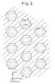
- the outlines of the GaN films are hexagons, as shown in Fig.2. Since individual GaN films enlarge at a common speed, the GaN films come in contact with the nearest neighbors simultaneously, as shown in Fig.3. The simultaneous contact is important.
- the individual films are integrated into a GaN film. The integrated GaN film begins to grow again upward for increasing the thickness.
- the windows are determined at the corners of equilateral triangles which cover the whole of the mask without blank.
- a set of sides of the hexagon is vertical to the y-axis (GaAs[11-2]). Other sets of the sides incline at 30 degrees to the y-axis.
- the hexagon has a set of sides vertical to GaAs[11-2], another set of sides parallel to GaAs[2-1-1] and a further set of sides parallel to GaAs[-12-1].
- the expression is done by basing upon GaAs orientation.
- the GaN crystal growing upon the GaAs substrate has different orientations from GaAs.
- GaAs belongs to the zinc blende type cubic symmetry group. Three parameters denote the orientations of GaAs. But GaN belongs to the hexagonal symmetry group which requires four parameters (klmn) for denoting the orientations.
- the three parameters k, l and m are not independent of each other, since the three parameters denote a orientation on c-plane.
- the final parameter n is an inverse of the segment cut by the object plane on c-axis.
- C-axis is vertical to a plane including a-, b- and d-axes.
- the hexagonal symmetry has six-fold rotation symmetry around c-axis.
- GaN c-axis is parallel to GaAs[111].
- GaAs(111) plane has three-fold symmetry.
- GaN(0001) plane is parallel to GaAs(111)plane.
- GaN[10-10] is parallel to GaAs[11-2].
- GaN[1-210] is parallel to GaAs[-110].
- the Inventors have succeeded in making a wide, thick GaN single crystal by growing GaN films on a masked GaAs substrate and etching away the mask and the GaAs substrate.
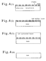
- Fig.4(1), Fig.4(2), Fig.4(3) and Fig.4(4) show the steps of the epitaxial growth of GaN.
- Fig.4(1) shows a GaAs substrate and a window-perforated mask.
- Fig.4(2) shows the step of growing a GaN buffer film on the GaAs within the windows at a lower temperature.
- Fig.4(3) shows a thick epitaxial GaN film growing slowly on the buffer layer at a higher temperature covering the mask.
- Fig.4(4) shows an isolated GaN substrate by etching away the GaAs substrate and polishing away the mask.
- the buffer layer includes plenty of microcrystals due to the low temperature growth.
- the later epitaxial film is grown at a high temperature for reducing defects.
- the final GaN is a freestanding wafer.
- the GaN has a width and a thickness enough to the substrate for devices. There are still some problems for the freestanding GaN substrate crystal. For example, the thickness, the strength, the size and
- the problem of the present invention is to control the conduction type of a GaN crystal.
- Prior GaN films have been made on a sapphire substrate mainly by an MOCVD method.
- Silicon (Si) is doped into the GaN for giving n-type conduction to the GaN crystal by the MOCVD.
- Silane gas (SiH 4 ) is the most accessible vapor compound including silicon (Si).
- the MOCVD supplies Si as an n-type dopant into the GaN film on a sapphire substrate.
- Silane gas is combustible, perilous gas which sometimes induces a sudden burst.
- Some safer n-dopant material than silane gas is desired for GaN. If the n-dopant has a high activation rate, the n-dopant is more desirable.
- n-dopant there is a hint on considering a new n-dopant.
- a non-doped GaN epitaxial film on sapphire reveals an n-type conduction property.
- a non-doped GaN film grown on a GaAs substrate by the lateral growth also reveals n-type conduction. Since Si is not doped, the n-dopant is not Si perhaps.
- a semiconductor is not necessarily intrinsic, even if an impurity is not intentionally doped. Even if an impurity is not doped, many semiconductors take either n-type or p-type.
- Non-doped Si is n-type.
- Non-doped GaAs is n-type.
- Non-doped GaN is n-type. Why can GaN be n-type despite non-doping?
- Another object of the present invention is to clarify the n-type conduction of non-doped GaN single crystal.
- Another object of the present invention is to provide a method of doping an n-type impurity into a GaN single crystal substrate other than silicon.
- a further object of the present invention is to provide a method of making an n-type GaN bulk single crystal.
- a further object of the present invention is to provide an n-type single crystal GaN substrate.
- the present invention achieves its object by providing a method of producing a gallium nitride single crystal substrate comprising the steps set out in claim 1.
- Oxygen as n-dopant has advantages over Si, a well-known n-dopant. Doping of silicon requires silane gas (SiH 4 ) or the like. But silane gas is a dangerous gas. Oxygen doping to GaN is far safer than silicon doping. Even in the case of doping nothing, oxygen included in material gases remains in the synthesized GaN crystal. The remaining oxygen acts as an n-dopant in GaN. The Inventors have confirmed that the n-carrier (electron) density can be easily controlled by doping oxygen into a GaN crystal. According to the invention, the n-carrier concentration is in proportion to the oxygen concentration.
- the inventors propose a GaN single crystal substrate having n-carrier density between 1 ⁇ 10 16 cm -3 and 1 ⁇ 10 20 cm - 3 based upon oxygen as an n-dopant.
- the n-carriers (electrons) are originated from oxygen as an n-dopant.
- the GaN substrate crystal of the present invention has an oxygen concentration ranging from 1 ⁇ 10 16 cm -3 to 1 ⁇ 10 20 cm -3 .
- the Inventors found out that carbon disturbs the function of oxygen as an n-type dopant.
- the carbon concentration should be suppressed below 1 ⁇ 10 18 cm -3 in the GaN crystal substrate of the invention.
- the carbon concentration should be below 1 ⁇ 10 17 cm -3 .
- This invention requires dangerous silane gas no more, because the invention does not use silicon as an n-type dopant.
- a GaN film is epitaxially grown upon some substrate, e.g., sapphire by a HVPE (halide vapor phase epitaxy) method from materials of metal Ga, hydrochloric gas (HCl) and ammonia gas (NH 3 ).
- HVPE halide vapor phase epitaxy
- the GaN film exhibits n-type conduction which has electrons as major carriers. Since Si is not included in the film, Si is not the n-dopant in the GaN. Some element except Si should be the n-dopant in the GaN film on the substrate. The fact is that oxygen atoms included as an impurity in material gases give the n-type conduction to the GaN film by supplying electrons in the film.
- oxygen is an n-type dopant.
- Non-doped GaN reveals n-type conduction.
- the n-type conduction is caused by oxygen originally included in the material gases, H 2 , HCl or NH 3 .
- the fact requires far strict control of oxygen as an impurity in the material gases for determining the carrier concentration exactly.
- Inventor's experiments reveal the inclusion of greater amount of oxygen as an impurity in the material gases than the skilled man imagines. If oxygen exhibited no function in GaN, the oxygen inclusion could be ignored. In fact, the oxygen inclusion should not be ignored, since oxygen acts as an n-dopant of supplying n-carriers (electrons) in a GaN crystal.
- This invention selects oxygen as an n-type dopant for GaN crystals instead of Si which has been introduced by the dangerous gas, silane. Oxygen doping is still safer than Si doping. Another advantage of oxygen is a high activation rate which is nearly equal to 100%. The activation rate is defined as a quotient of the carrier number to the dopant number. Perhaps, oxygen atoms form shallow donor levels which easily give an electron to a GaN crystal.
- oxygen exhibits a high activation rate in a wide range of concentration.
- Oxygen acts as an n-dopant with a high activation rate in a wide range of oxygen concentration between 1 ⁇ 10 16 cm -3 and 1 ⁇ 10 20 cm -3 .
- the range of the oxygen concentration gives a carrier (electron) concentration ranging between 1 ⁇ 10 16 cm -3 and 1 ⁇ 10 20 cm - 3 , because the activation rate is nearly 100%.
- Some method adopts metallorganic materials, e.g., trimethyl Ga(TMG) for Ga-including material gas.
- An MOCVD metalorganic chemical vapor deposition
- carbon atoms borne by the dissociation of metallorganic compounds remain in the crystal as an impurity.
- the Inventors found the fact that the residual carbon atoms in the GaN crystal induce instability of carriers. Sometimes carbon atoms act as donors making n-type carriers (electrons). Other times carbon atoms make deep trap levels which cancel other donors. The instability induced by the residual carbon is a nuisance for the exact control of carriers.
- the Inventors are aware of a decline of the intensity of photoluminescence in a GaN film at a high carbon concentration more than 1 ⁇ 10 18 cm -3 .
- the residual carbon atoms in the GaN should be suppressed to a small concentration of less than 1 ⁇ 10 18 cm -3 , preferably less than 10 17 cm -3 for allowing oxygen to act effectively as an n-dopant.
- the Inventors first noticed that the growth of a GaN film on a GaAs substrate enables us to control the carbon concentration in the GaN.
- This invention clarifies that oxygen is an excellent n-dopant with an activation rate of nearly 100% in a GaN crystal for the first time.
- This invention adopts oxygen (O) as an n-dopant instead of silicon (Si).
- This invention allows exact control of the n-carrier concentration in a GaN crystal by adding O or H 2 O into material gases at a suitable ratio. Since the activation rate is nearly 100% in a wide range from 1 ⁇ 10 16 cm -3 to 1 ⁇ 10 20 cm -3 of oxygen concentration, this invention enables manufacturers to produce a GaN single freestanding crystal of an arbitrary carrier density between 1 ⁇ 10 16 cm -3 to 1 ⁇ 10 20 cm -3 .
- the preferable range is 5 ⁇ 10 17 cm -3 to 5 ⁇ 10 19 cm -3 for both the oxygen concentration and the carrier concentration.
- the optimum concentration ranges from 1 ⁇ 10 18 cm -3 to 1 ⁇ 10 19 cm -3 both for oxygen and carriers.
- An increase of the carrier concentration raises the conductivity of the GaN.
- Low resistance is a favorable property as a substrate crystal.
- the upper limit is determined by the crystalline disorder caused by doping high density oxygen.
- GaN films have been piled epitaxially upon a sapphire substrate by the MOCVD method for fabricating blue light LEDs.
- the MOCVD uses silane gas (SiH 4 ) for doping Si as an n-dopant into a GaN film on the sapphire.
- Silane is a dangerous gas.
- This invention is immune from the danger by adopting safe oxygen gas as an n-dopant.
- This invention can produce an n-type GaN bulk single crystal by growing GaN films on a masked GaAs substrate and eliminating the GaAs and the mask.
- the bulk GaN crystal has n-type conduction due to the doped oxygen.
- the bottom of the GaN substrate can be an n-electrode for directly bonded and connected to a stem.
- the LED device structure is simplified in comparison with the sapphire-based GaInN-LED. If a GaInN laser diode is fabricated on the n-GaN substrate, the blue light laser diode has a longer lifetime than the conventional sapphire-based blue light laser diode.
- GaN crystals can be produced on a substrate by the following four methods;
- the HVPE method selects metal gallium (Ga) as a Ga material.
- the HVPE once makes an intermediate compound (GaCl) by a reaction 2Ga + 2HCl ⁇ 2GaCl + H 2 and produces the object gallium nitride (GaN) from the gallium chloride (GaCl) and ammonia (NH 3 ) by another reaction GaCl + NH 3 ⁇ GaN + HCl + H 2 .
- This method is named "halide", since gallium chloride (GaCl), a halide, is once synthesized.
- the MOC method chooses metallorganic gallium, e.g., trimethyl gallium (Ga(CH 3 ) 3 ), as a Ga material.
- the MOC produces an intermediate compound (GaCl) by a reaction Ga(CH 3 ) 3 +HCl ⁇ GaCl+ ⁇ .
- the MOC makes GaN on a substrate from GaCl and NH 3 by another reaction GaCl + NH 3 ⁇ GaN + HCl + H 2 .
- the MOC is not a popular method. No other than the Applicant makes a GaN film epitaxially on a GaAs substrate at a temperature higher than 900°C by the MOC method.
- the MOCVD method chooses metallorganic gallium as a Ga material like the MOC.
- the MOCVD is different from the HVPE and the MOC at the points of omitting the intermediate process.
- the MOCVD makes GaN at a stretch by reacting the metallorganic Ga with ammonia by a reaction Ga(CH 3 ) 3 + NH 3 ⁇ GaN + ⁇ .
- the MOCVD is a prevailing method. Almost all of the GaN epitaxial growths are done by the MOCVD method at present.
- the sublimation method starts from polycrystal GaN. It makes a GaN single crystal film on a substrate by keeping the substrate at a lower temperature, heating the polycrystal material at a higher temperature for subliming the polycrystal into vapor and transporting the vapor to the substrate by the gradient of the temperature.
- This invention turns out to be suitable for 1.HVPE method and 2.MOC method but unsuitable for the most prevalent 3.MOCVD method.
- This invention cannot be applied to the popular MOCVD method. Namely, the MOCVD method cannot realize this invention, because the MOCVD adopts metallorganic Ga and lacks the step of making the intermediate compound GaCl which has a function of eliminating carbon.
- carbon atoms sometimes act as an n-dopant or a p-dopant and other times act as a neutral impurity in a GaN crystal.
- the roles of carbon are ambiguous and unstable in GaN. When carbon is included in a GaN crystal, the n-carrier density is not in proportion to the oxygen concentration.
- the density of residual carbon should be suppressed at most less than 10 18 cm -3 for allowing oxygen atoms to act as an n-dopant making shallow donor levels and for maintaining the proportional relation between the oxygen concentration and the electron concentration.
- the substantially non-carbon ⁇ 10 18 cm -3 , preferably ⁇ 10 17 cm - 3
- the MOCVD cannot prevent the carbon contained in trimethyl Ga from mixing into the GaN film. Slow growth allows the MOCVD to prevent carbon from mixing into GaN.
- This invention is suitable for the HVPE or the MOC producing GaN via the intermediate gallium chloride (GaCl).
- the intermediate GaCl vapor enables both the HVPE and the MOC to exclude carbon atoms completely or nearly completely from the GaN crystal by refining the material gases deliberately.
- the oxygen concentration is proportional to the free electron (n-carrier) concentration in the HVPE-made or MOC-made GaN crystal.
- Exact prescription of oxygen in the material gas is essential for controlling the n-carriers by the doping oxygen. For this reason, oxygen and water should be completely removed from material gases by repeated refinements till the oxygen density and the water density attain values below the detectable limits. After the complete refinement, a desired number of oxygen or water molecules are added to the material gases.
- Oxygen gas or water is available for doping oxygen. Oxygen or water should be added to a congenial gas. Both the MOC and the HVPE use HCl gas, H 2 , gas and NH 3 gas. The MOC further uses trimethyl Ga gas bubbled and carried by H 2 . It is convenient to add oxygen or water to H 2 gas (carrier gas), HCl gas or NH 3 gas. Oxygen or water contained in HCl produces gallium oxide (Ga 2 O) by reacting with the metal Ga or the metallorganic Ga. The Ga 2 O effectively is taken into the synthesized GaN film.
- a GaAs(111) wafer is prepared for a substrate crystal.
- a silicon dioxide (SiO 2 ) insulating film is formed uniformly upon the GaAs(111)A plane.
- Photolithography perforates a plenty of dottedly-populated square windows on the SiO 2 mask for revealing the undercoat GaAs surface partially within the windows, as shown in Fig. 1.
- Each window is a square of a 2 ⁇ m long side.
- a second set of windows align with a half period shift with the same period in series in the same direction as the former set.
- a third set of windows align with a half period shift with the same period in the same direction as the former sets. Similar alignments of windows are repeated on the mask.
- the centers of the nearest neighboring three windows form an equilateral triangle of a 4 ⁇ m long side in parallel with ⁇ 11-2>. This step makes a masked GaAs wafer substrate.
- a GaN buffer layer is piled till a thickness of 80nm at a comparatively low temperature of about 490 °C upon the masked GaAs substrate by the HVPE apparatus. Then, the wafer is further heated up to a temperature between 920°C and 1050°C. A GaN epitaxial layer is further piled on the buffer layer and the mask till a thickness of about 200 ⁇ m by the same HVPE apparatus.
- the growing conditions and the thicknesses of the GaN buffer layer and the GaN epitaxial layer are as follows; (GaN buffer layer) 490°C 80nm (GaN epitaxial layer) 920°C ⁇ 1050°C 200 ⁇ m
- the orientation of the GaN nuclei is determined by the orientation of the undercoat GaAs crystal.
- GaN single crystal grains gradually grow from the GaN nuclei.
- the orientations of the grains are ruled by the undercoat GaAs. All the grains have the common orientation through the undercoat GaAs single crystal substrate.
- the GaN grains fill the windows of the mask. When the GaN grain crystals have filled the windows, the GaN crystals overflow upon the mask from the windows and develop on the mask in hexagons according to the crystal orientation of the undercoat GaAs, as shown in Fig.2.
- the overflowing GaN films also have the similar orientation to the undercoat GaAs.
- the isolated GaN films from the windows come into contact with the other films growing from the neighboring windows, as shown in Fig.3. Since all the isolated films are growing from their own windows at the same velocity in hexagons, the joints of the neighboring films form many hexagons like a honeycomb.
- the isolated films are integrated into a single film. Then the height of the integrated GaN film further increases in the HVPE apparatus.
- Embodiment 1 chooses the HVPE (Halide Vapor Phase Epitaxy) method for making the GaN crystal.
- the HVPE method comprises the steps of preparing a quartz boat having metal Ga, storing the Ga-containing boat in the reaction furnace, heating the boat up to more than 800 °C , supplying hydrochloric gas (HCl) on the metal Ga in the furnace for synthesizing gallium chloride (GaCI), supplying ammonia gas NH 3 to the GaAs substrate wafer for making NH 3 react with the GaCl and growing GaN on the substrate.
- the carrier gas is hydrogen both for HCl and NH 3 .
- Fig.5 shows a section of the HVPE apparatus.
- the HVPE apparatus has a vertically elongating furnace 1.
- the vertical furnace 1 is equipped with a cylindrical heater 2.
- Shorter and longer material gas inlet tubes 3 and 4 are inserted at the top of the furnace 1.
- the shorter material gas inlet tube 3 introduces hydrochloric gas (HCl) and hydrogen gas (H 2 ).
- Hydrogen gas is a carrier gas for HCl.
- the longer material gas inlet tube 4 introduces ammonia gas (NH 3 ) and hydrogen gas (H 2 ).
- Hydrogen gas is a carrier gas for NH 3 .
- the furnace 1 contains a Ga boat 5 just beneath the shorter material gas inlet tube 3.
- a Ga-melt 6 is filled in the Ga boat 5.
- a shaft 8 vertically pierces the bottom of the furnace 1.
- the shaft 8 can rotate and move up and down in the furnace 1.
- the shaft 8 holds a susceptor 7 on its top.
- a GaAs wafer 9 is put on the susceptor 7.
- the furnace 1 is provided with an exhaustion outlet 10 at the bottom for making the furnace vacuous.
- the exhaustion outlet 10 communicates with a vacuum pump (not shown in the figures).
- HCl gas and H 2 gas go into the furnace 1 from the gas inlet 3.
- NH 3 gas and H 2 gas are introduced to the furnace 1 from the gas inlet 4.
- HCl gas reacts with the Ga melt 6 for making gallium chloride (GaCl). The reaction is expressed by 2Ga + 2HCl ⁇ 2GaCl + H 2 .
- the HVPE method adopts metal Ga as the Ga-source.
- Metal Ga is a melt in the furnace.
- the HVPE Hydrochloric gas
- GaCl gallium chloride
- HCl hydrochloric gas
- GaCl takes vapor phase at a high temperature.
- Hydrogen gas can convey the GaCl gas from the Ga-boat to the object GaAs substrate.
- This method is called "halide" VPE, since it uses a "chloride” of Ga as Ga-material.
- the HVPE does not use metallorganic compounds.
- the difference among the HVPE, MOC and MOCVD is the difference of the Ga-material.
- the N-material is ammonia (NH 3 ) which is common for the three methods.
- HCl gas in general, includes oxygen and water as an impurity. Only repetitions of refinements exclude oxygen and water from HCl gas.
- the GaAs wafer is cooled.
- the GaAs wafer is taken out of the furnace.
- a continual mirror film of GaN coats the GaAs substrate.
- the substrate has a hybrid stratum structure of GaN/GaAs.
- Aqua regia can solve GaAs.
- the GaAs substrate is eliminated in aqua regia.
- GaN has resistance against aqua regia. Thus, only the GaN film remains.
- the GaN film has a thickness of about 200 ⁇ m.
- the GaN crystal film is freestanding due to the sufficient thickness.
- the freestanding GaN film is a single crystal.
- the single crystal GaN can be a GaN substrate for making GaN-like devices.
- a plurality of GaN substrate crystals are produced by the method of the embodiment 1 by taking three kinds of HCl gases (a), (b) and (c) for investigating the relation between n-carrier (electron) concentration and oxygen concentration.
- the oxygen concentration and the n-carrier concentration in the sample GaN substrate crystals are measured.
- the oxygen concentration is measured by the SIMS (Secondary Ion-Mass Spectrography) which bombards the sample GaN substrate crystals with ions of inert gas, induces emission of secondary ions from the object GaN substrate crystals, counts the ions in divided ranges of energy, makes a spectrum of the secondary ions and calculates the ratios of the elements existing in the sample.
- the concentration of n-carriers (electrons) is determined by the Hall measurement.
- the separated GaN substrate crystals reveal n-type conduction although Si is not doped into the GaN. Instead of Si, O acts as an n-type impurity for giving the n-type conduction to the GaN crystal.
- the electron (n-carrier) density is in proportion to the oxygen density.
- the carrier gas, hydrogen contains oxygen or water.
- the nitrogen-source, ammonia also contains oxygen or water. Then, the influence of water accompanies even the case of using purified HCl (c).
- a GaN crystal is made on a GaAs substrate by a similar manner to embodiment 1. Namely, a GaN buffer layer and a GaN epitaxial layer are produced upon a masked GaAs wafer by a HVPE method supplying HCl+H 2 to a Ga melt for converting Ga to GaCl and supplying NH 3 + H 2 for making NH 3 react with GaCl, and making GaN on the GaAs substrate.
- Embodiment 2 differs from embodiment 1 at the HCl + H 2 gas which is supplied to the Ga-melt. Instead of HCl including water, hydrogen H 2 gas contains water. The prepared gases are;
- a mixture of (d) and (e) at an arbitrary rate is supplied to the heated Ga-melt in the HVPE furnace.
- the rate H 2 O/HCl is continually varied in a range between 0 and 3000 ppm. Namely, 0 ⁇ H 2 O/HCl ⁇ 3000ppm.
- water (H 2 O) included in H 2 gas oxygen mixes into GaCl.
- An isolated GaN substrate is obtained by solving the GaAs substrate by aqua regia.
- the GaN substrate reveals n-type conduction despite of non-existence of Si.
- the carrier density is in proportion to the oxygen density.
- Embodiment 2 confirms that oxygen acts as an n-type impurity in GaN and water in H 2 is also effective for giving n-type conduction to GaN.
- Embodiment 3 makes a GaN single crystal film upon a masked GaAs substrate wafer in a similar way to embodiment 1.
- a GaN buffer layer and a GaN epitaxial layer are grown by the HVPE method on a GaAs substrate by utilizing a mask having windows positioned at corners of equilateral triangles.
- the HCl gas is different from that of embodiment 1. Instead of water, oxygen is intentionally added to the HCl gas.
- Embodiment 3 introduces oxygen into the GaCl gas through the HCl gas. Prepared gases are;
- a mixture (HCl+O 2 ) of (f) and (g) at an arbitrary rate is supplied to the heated Ga-melt in the HVPE furnace.
- the rate O 2 /HCl is continually varied in a range between 0 and 3000 ppm. Namely, 0 ⁇ O 2 /HCl ⁇ 3000ppm.
- oxygen included in HCl mixes into GaCl gas.
- a freestanding GaN substrate crystal is obtained by solving the GaAs substrate and the mask by aqua regia.
- the produced GaN substrate reveals n-type conduction.
- the carrier density is in proportion to the oxygen density.
- Embodiment 3 confirms that oxygen acts as an n-type impurity in GaN and O 2 included in HCl gas is also effective for giving n-type conduction to GaN.
- Embodiment 4 makes a GaN single crystal film upon a masked GaAs substrate wafer in a similar way to embodiment 1.
- a GaN buffer layer and a GaN epitaxial layer are grown by the HVPE method on a GaAs substrate by utilizing a mask having windows positioned at corners of equilateral triangles.
- the NH 3 gas is different from that of embodiment 1.
- water is intentionally added to the H 2 carrier gas of NH 3 .
- NH 3 gas substantially includes water (H 2 O).
- Embodiment 4 introduces oxygen into the GaCl gas through the NH 3 gas. Prepared gases are;
- a mixture (NH 3 +H 2 ) of (h) and (i) at an arbitrary rate is supplied to react with GaCl in the HVPE furnace. It is not always necessary to guide all the carrier hydrogen gas into the bubbler. It is enough to make a part of hydrogen gas pass through the bubbler for making humid NH 3 .
- the ratio of water in the humid ammonia gas is changed by controlling the temperature of the bubbler.
- the rate of H 2 O/(H 2 +NH 3 ) is continually varied in a range between 5 ppm and 50 ppm. Namely, 5ppm ⁇ H 2 O/(H 2 +NH 3 ) ⁇ 50ppm.
- the ratio of H 2 O/(H 2 +NH 3 ) is smaller than the case of adding water to HCl gas. It is verified that oxygen is effectively included in the GaN crystal, even if the ratio of H 2 O/(H 2 +NH 3 ) is small.
- Embodiment 5 makes a GaN single crystal film upon a masked GaAs substrate wafer in a similar way to embodiment 1.
- a GaN buffer layer and a GaN epitaxial layer are grown by the HVPE method on a GaAs substrate by utilizing a mask having windows positioned at corners of equilateral triangles.
- the NH 3 gas is different from that of embodiment 1.
- oxygen (O 2 ) is intentionally added to NH 3 .
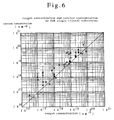
- Fig.6 shows the result of measurements of oxygen concentration and n-carrier concentration in 38 samples of embodiments 1 to 5.
- the n-carrier is an electron.
- the abscissa is oxygen concentration (O) (cm -3 ).
- the ordinate is carrier concentration (n) (cm -3 ).
- One sample corresponds to one dot.
- carrier concentration is one of the objects which are frequently measured in semiconductor researches.
- the carrier density can be easily measured by the Hall measurement.
- the concentration of oxygen is not an object which is frequently measured.
- the oxygen measurement of the SIMS is not a facile measurement. Thus, nobody has noticed the possibility of oxygen donors before this invention.
- the oxygen concentration also depends upon the growing temperature (T) and the growing speed (v) of GaN.
Landscapes
- Chemical & Material Sciences (AREA)
- Engineering & Computer Science (AREA)
- Crystallography & Structural Chemistry (AREA)
- Materials Engineering (AREA)
- Metallurgy (AREA)
- Organic Chemistry (AREA)
- Chemical Kinetics & Catalysis (AREA)
- General Chemical & Material Sciences (AREA)
- Inorganic Chemistry (AREA)
- Crystals, And After-Treatments Of Crystals (AREA)
Claims (7)
- Procédé de fabrication d'un substrat monocristallin de nitrure de gallium comprenant les étapes consistant à :préparer un substrat de GaAs (111), en recouvrant le substrat de GaAs avec un masque et en gravant le masque pour fabriquer des fenêtres ;raffiner les gaz servant de matériaux HCl, NH3 et H2 jusqu'à ce que l'oxygène (O2) et l'eau (H2O) soient retirés pour atteindre des valeurs inférieures aux limites détectables ;introduire les gaz servant de matériaux HCl, NH3 et H2 dans une chambre de réaction pourassurer la croissance d'une couche tampon de GaN sur le substrat de GaAs masqué grâce à un procédé d'EPVH (épitaxie en phase vapeur aux halogénures) ou un procédé d'EPVCO (épitaxie en phase vapeur aux chlorures organométalliques) comprenant un premier procédé via-GaCl qui fabrique du GaCl à partir d'un matériau de Ga et de HCl et fait réagir le GaCl avec le NH3 pour produire du GaN ; et pourassurer la croissance d'une couche épitaxiale de GaN sur ladite couche tampon de GaN grâce à un procédé d'EPVH ou un procédé d'EPVCO comprenant un deuxième procédé via-GaCl qui fabrique du GACl à partir d'un matériau de Ga et de HCl, fait réagir le GACl avec le NH3 pour produire du GaN, dans lequel, à l'étape consistant à assurer la croissance d'une couche épitaxiale, après ladite étape de raffinage, l'oxygène (O2) ou l'eau (H2O) est ajouté selon un rapport adéquat aux gaz servant de matériaux HCl, NH3 et H2 devant être introduits pour permettre le contrôle de la concentration en porteurs n dans le cristal de GaN ;retirer le substrat de GaAs et le masque ; etobtenir un substrat monocristallin de GaN de type n autoporté ayant de l'oxygène comme dopant n.
- Procédé selon la revendication 1, dans lequel le masque a des fenêtres en pointillés se trouvant au niveau de points qui correspondent aux angles de triangles équilatéraux ayant un côté parallèle à la direction [11-2] du substrat de GaAs et couvrant la surface du masque sans interstices.
- Procédé selon la revendication 1, dans lequel le masque a des fenêtres rayées parallèles qui sont parallèles à l'une ou l'autre des directions [11-2] et [1-10] du substrat de GaAs.
- Procédé selon la revendication 1, dans lequel le premier procédé via-GaCl est un procédé d'EPVH qui utilise du Ga métallique, du HCl, du H2 et du NH3 comme matériaux, fabrique du GaCl à partir du Ga métallique et du HCl, et produit du GaN en faisant réagir le GaCl avec le NH3.
- Procédé selon la revendication 1, dans lequel le deuxième procédé via-GaCl est un procédé d'EPVH qui utilise du Ga métallique, du HCl, du H2 et du NH3 comme matériaux, fabrique du GaCl à partir du Ga métallique et du HCl, et produit du GaN en faisant réagir le GaCl avec le NH3.
- Procédé selon la revendication 1, dans lequel le premier procédé via-GaCl est un procédé d'EPVCO qui utilise du Ga métallorganique, du HCl, du H2 et du NH3 comme matériaux, fabrique du GaCl à partir du Ga métallorganique et du HCl, et produit du GaN en faisant réagir le GaCl avec le NH3.
- Procédé selon la revendication 1, dans lequel le deuxième procédé via-GaCl est un procédé d'EPVCO qui utilise du Ga métallorganique, du HCl, du H2 et du NH3 comme matériaux, fabrique du GaCl à partir du Ga métallorganique et du HCl, et produit du GaN en faisant réagir le GaCl avec le NH3.
Priority Applications (3)
| Application Number | Priority Date | Filing Date | Title |
|---|---|---|---|
| EP06015516.5A EP1739759A3 (fr) | 1998-05-28 | 1999-05-26 | Substrat monocristallin de nitrure de gallium et procédé de fabrication |
| EP06018999A EP1739760A2 (fr) | 1998-05-28 | 1999-05-26 | Substrat monocristallin de nitrure de gallium et procédé de fabrication |
| EP06006946A EP1672708A3 (fr) | 1998-05-28 | 1999-05-26 | Substrat monocristallin de nitrure de gallium |
Applications Claiming Priority (2)
| Application Number | Priority Date | Filing Date | Title |
|---|---|---|---|
| JP14771698 | 1998-05-28 | ||
| JP14771698 | 1998-05-28 |
Related Child Applications (3)
| Application Number | Title | Priority Date | Filing Date |
|---|---|---|---|
| EP06006946A Division EP1672708A3 (fr) | 1998-05-28 | 1999-05-26 | Substrat monocristallin de nitrure de gallium |
| EP06015516.5A Division EP1739759A3 (fr) | 1998-05-28 | 1999-05-26 | Substrat monocristallin de nitrure de gallium et procédé de fabrication |
| EP06018999A Division EP1739760A2 (fr) | 1998-05-28 | 1999-05-26 | Substrat monocristallin de nitrure de gallium et procédé de fabrication |
Publications (2)
| Publication Number | Publication Date |
|---|---|
| EP0967664A1 EP0967664A1 (fr) | 1999-12-29 |
| EP0967664B1 true EP0967664B1 (fr) | 2006-09-13 |
Family
ID=15436590
Family Applications (4)
| Application Number | Title | Priority Date | Filing Date |
|---|---|---|---|
| EP06015516.5A Withdrawn EP1739759A3 (fr) | 1998-05-28 | 1999-05-26 | Substrat monocristallin de nitrure de gallium et procédé de fabrication |
| EP06018999A Withdrawn EP1739760A2 (fr) | 1998-05-28 | 1999-05-26 | Substrat monocristallin de nitrure de gallium et procédé de fabrication |
| EP99110229A Expired - Lifetime EP0967664B1 (fr) | 1998-05-28 | 1999-05-26 | Substrat monocristallin de nitrure de gallium et procédé de fabrication |
| EP06006946A Withdrawn EP1672708A3 (fr) | 1998-05-28 | 1999-05-26 | Substrat monocristallin de nitrure de gallium |
Family Applications Before (2)
| Application Number | Title | Priority Date | Filing Date |
|---|---|---|---|
| EP06015516.5A Withdrawn EP1739759A3 (fr) | 1998-05-28 | 1999-05-26 | Substrat monocristallin de nitrure de gallium et procédé de fabrication |
| EP06018999A Withdrawn EP1739760A2 (fr) | 1998-05-28 | 1999-05-26 | Substrat monocristallin de nitrure de gallium et procédé de fabrication |
Family Applications After (1)
| Application Number | Title | Priority Date | Filing Date |
|---|---|---|---|
| EP06006946A Withdrawn EP1672708A3 (fr) | 1998-05-28 | 1999-05-26 | Substrat monocristallin de nitrure de gallium |
Country Status (7)
| Country | Link |
|---|---|
| US (1) | US20020011599A1 (fr) |
| EP (4) | EP1739759A3 (fr) |
| JP (1) | JP2010132556A (fr) |
| KR (1) | KR100406216B1 (fr) |
| CN (1) | CN1148810C (fr) |
| DE (1) | DE69933169T2 (fr) |
| TW (1) | TW428331B (fr) |
Families Citing this family (68)
| Publication number | Priority date | Publication date | Assignee | Title |
|---|---|---|---|---|
| US7560296B2 (en) * | 2000-07-07 | 2009-07-14 | Lumilog | Process for producing an epitalixal layer of galium nitride |
| TW417315B (en) * | 1998-06-18 | 2001-01-01 | Sumitomo Electric Industries | GaN single crystal substrate and its manufacture method of the same |
| JP3007971B1 (ja) * | 1999-03-01 | 2000-02-14 | 東京大学長 | 単結晶薄膜の形成方法 |
| US6773504B2 (en) * | 2001-04-12 | 2004-08-10 | Sumitomo Electric Industries, Ltd. | Oxygen doping method to gallium nitride single crystal substrate and oxygen-doped N-type gallium nitride freestanding single crystal substrate |
| US8633093B2 (en) | 2001-04-12 | 2014-01-21 | Sumitomo Electric Industries Ltd. | Oxygen doping method to gallium nitride single crystal substrate |
| JP4116535B2 (ja) * | 2001-06-06 | 2008-07-09 | アンモノ・スプウカ・ジ・オグラニチョノン・オドポヴィエドニアウノシツィオン | ガリウム含有窒化物の単結晶の製造法及び装置 |
| US7057211B2 (en) * | 2001-10-26 | 2006-06-06 | Ammono Sp. Zo.O | Nitride semiconductor laser device and manufacturing method thereof |
| US7097707B2 (en) * | 2001-12-31 | 2006-08-29 | Cree, Inc. | GaN boule grown from liquid melt using GaN seed wafers |
| US6791120B2 (en) * | 2002-03-26 | 2004-09-14 | Sanyo Electric Co., Ltd. | Nitride-based semiconductor device and method of fabricating the same |
| US20060138431A1 (en) | 2002-05-17 | 2006-06-29 | Robert Dwilinski | Light emitting device structure having nitride bulk single crystal layer |
| WO2004051759A1 (fr) * | 2002-12-03 | 2004-06-17 | Nec Corporation | Dispositif optique a semi-conducteur avec structure de puits quantique et son procede de fabrication |
| ATE445722T1 (de) * | 2002-12-11 | 2009-10-15 | Ammono Sp Zoo | Schabloneartiges substrat und verfahren zu seiner herstellung |
| TWI334890B (en) * | 2002-12-11 | 2010-12-21 | Ammono Sp Zoo | Process for obtaining bulk mono-crystalline gallium-containing nitride, eliminating impurities from the obtained crystal and manufacturing substrates made of bulk mono-crystalline gallium-containing nitride |
| WO2004061923A1 (fr) * | 2002-12-27 | 2004-07-22 | General Electric Company | Cristal de nitrure de gallium, dispositifs a base de nitrure de gallium homoepitaxial et procede de production associe |
| US7524691B2 (en) * | 2003-01-20 | 2009-04-28 | Panasonic Corporation | Method of manufacturing group III nitride substrate |
| US7261777B2 (en) * | 2003-06-06 | 2007-08-28 | S.O.I.Tec Silicon On Insulator Technologies | Method for fabricating an epitaxial substrate |
| EP1484794A1 (fr) * | 2003-06-06 | 2004-12-08 | S.O.I. Tec Silicon on Insulator Technologies S.A. | Procédé de fabrication d'un substrat auto-porté |
| JP3841092B2 (ja) | 2003-08-26 | 2006-11-01 | 住友電気工業株式会社 | 発光装置 |
| JP4534631B2 (ja) * | 2003-10-31 | 2010-09-01 | 住友電気工業株式会社 | Iii族窒化物結晶の製造方法 |
| JP2005191530A (ja) * | 2003-12-03 | 2005-07-14 | Sumitomo Electric Ind Ltd | 発光装置 |
| EP1727177B1 (fr) | 2004-03-12 | 2017-01-04 | Hamamatsu Photonics K.K. | Procédé de fabrication d' un élément stratifié photoélectrique et élément stratifié |
| US7303632B2 (en) * | 2004-05-26 | 2007-12-04 | Cree, Inc. | Vapor assisted growth of gallium nitride |
| KR100848380B1 (ko) * | 2004-06-11 | 2008-07-25 | 암모노 에스피. 제트오. 오. | 갈륨 함유 질화물의 벌크 단결정 및 그의 어플리케이션 |
| JP4525309B2 (ja) * | 2004-11-19 | 2010-08-18 | 日立電線株式会社 | Iii−v族窒化物系半導体基板の評価方法 |
| PL371405A1 (pl) * | 2004-11-26 | 2006-05-29 | Ammono Sp.Z O.O. | Sposób wytwarzania objętościowych monokryształów metodą wzrostu na zarodku |
| JP4384019B2 (ja) * | 2004-12-08 | 2009-12-16 | 住友電気工業株式会社 | ヘッドランプ |
| CA2563731A1 (fr) * | 2005-03-04 | 2006-09-08 | Sumitomo Electric Industries, Ltd. | Dispositif semi-conducteur de nitrure de gallium vertical et substrat epitaxial |
| CN1988109B (zh) * | 2005-12-21 | 2012-03-21 | 弗赖贝格化合物原料有限公司 | 生产自支撑iii-n层和自支撑iii-n基底的方法 |
| KR101374090B1 (ko) * | 2007-07-26 | 2014-03-17 | 아리조나 보드 오브 리젠츠 퍼 앤 온 비하프 오브 아리조나 스테이트 유니버시티 | 에피택시 방법들과 그 방법들에 의하여 성장된 템플릿들 |
| US8026718B2 (en) * | 2007-08-28 | 2011-09-27 | Ngk Insulators, Ltd. | Magnetic sensor, hall element, hall IC, magnetoresistive effect element, method of fabricating hall element, and method of fabricating magnetoresistive effect element |
| JP2009167066A (ja) * | 2008-01-18 | 2009-07-30 | Sumitomo Electric Ind Ltd | 窒化ガリウムの結晶成長方法および窒化ガリウム基板の製造方法 |
| JP4375497B1 (ja) * | 2009-03-11 | 2009-12-02 | 住友電気工業株式会社 | Iii族窒化物半導体素子、エピタキシャル基板、及びiii族窒化物半導体素子を作製する方法 |
| JP4513927B1 (ja) * | 2009-09-30 | 2010-07-28 | 住友電気工業株式会社 | Iii族窒化物半導体基板、エピタキシャル基板及び半導体デバイス |
| JP5365454B2 (ja) | 2009-09-30 | 2013-12-11 | 住友電気工業株式会社 | Iii族窒化物半導体基板、エピタキシャル基板及び半導体デバイス |
| US8592292B2 (en) * | 2010-09-02 | 2013-11-26 | National Semiconductor Corporation | Growth of multi-layer group III-nitride buffers on large-area silicon substrates and other substrates |
| US9076827B2 (en) | 2010-09-14 | 2015-07-07 | Applied Materials, Inc. | Transfer chamber metrology for improved device yield |
| WO2012102970A1 (fr) * | 2011-01-24 | 2012-08-02 | Applied Materials, Inc. | Croissance d'empilements de led iii-v au moyen de nanomasques |
| JP5826698B2 (ja) * | 2011-04-13 | 2015-12-02 | 株式会社アルバック | Ni膜の形成方法 |
| CN102140680A (zh) * | 2011-05-10 | 2011-08-03 | 青岛铝镓光电半导体有限公司 | 氮化镓单晶的制备方法 |
| KR101976229B1 (ko) | 2011-10-21 | 2019-05-07 | 미쯔비시 케미컬 주식회사 | 주기표 제 13 족 금속 질화물 반도체 결정의 제조 방법, 및 그 제조 방법에 의해 제조되는 주기표 제 13 족 금속 질화물 반도체 결정 |
| US8569153B2 (en) * | 2011-11-30 | 2013-10-29 | Avogy, Inc. | Method and system for carbon doping control in gallium nitride based devices |
| JP2013145867A (ja) * | 2011-12-15 | 2013-07-25 | Hitachi Cable Ltd | 窒化物半導体テンプレート及び発光ダイオード |
| WO2014129544A1 (fr) | 2013-02-22 | 2014-08-28 | 三菱化学株式会社 | Cristal de nitrure de métal du groupe 13 du tableau périodique, et son procédé de production |
| US9970126B2 (en) | 2013-02-26 | 2018-05-15 | Massachusetts Institute Of Technology | Production of free-standing crystalline material layers |
| JP6330899B2 (ja) * | 2013-03-27 | 2018-05-30 | ベイジン トンメイ クリスタル テクノロジー カンパニー リミテッド | 半導体基板中の制御可能な酸素濃度 |
| US9312446B2 (en) | 2013-05-31 | 2016-04-12 | Ngk Insulators, Ltd. | Gallium nitride self-supported substrate, light-emitting device and manufacturing method therefor |
| KR101790458B1 (ko) | 2014-03-31 | 2017-10-25 | 엔지케이 인슐레이터 엘티디 | 다결정 질화갈륨 자립 기판 및 그것을 이용한 발광 소자 |
| JP6342703B2 (ja) * | 2014-05-09 | 2018-06-13 | 古河機械金属株式会社 | 自立基板の製造方法及び自立基板 |
| WO2016051890A1 (fr) | 2014-09-29 | 2016-04-07 | 日本碍子株式会社 | Substrat autoporteur de nitrure de gallium, élément luminescent et leurs procédés de production |
| JP6578570B2 (ja) * | 2015-03-03 | 2019-09-25 | 国立大学法人大阪大学 | Iii族窒化物半導体結晶基板の製造方法 |
| DE102015205104A1 (de) * | 2015-03-20 | 2016-09-22 | Freiberger Compound Materials Gmbh | Züchtung von A-B Kristallen ohne Kristallgitter-Krümmung |
| US20160284957A1 (en) * | 2015-03-23 | 2016-09-29 | Toshiba Corporation | REFLECTIVE CONTACT FOR GaN-BASED LEDS |
| JP6688109B2 (ja) | 2016-02-25 | 2020-04-28 | 日本碍子株式会社 | 面発光素子、外部共振器型垂直面発光レーザー、および面発光素子の製造方法 |
| US10541514B2 (en) | 2016-02-25 | 2020-01-21 | Ngk Insulators, Ltd. | Surface-emitting device, vertical external-cavity surface-emitting laser, and method for manufacturing surface-emitting device |
| JP6648253B2 (ja) | 2016-02-25 | 2020-02-14 | 日本碍子株式会社 | 多結晶窒化ガリウム自立基板及びそれを用いた発光素子 |
| US10749070B2 (en) * | 2016-05-20 | 2020-08-18 | Lumileds Llc | Method of forming a P-type layer for a light emitting device |
| US10648102B2 (en) * | 2017-01-09 | 2020-05-12 | Slt Technologies, Inc. | Oxygen-doped group III metal nitride and method of manufacture |
| JP6356315B1 (ja) | 2017-05-29 | 2018-07-11 | 株式会社サイオクス | 窒化物結晶基板、半導体積層物、半導体積層物の製造方法および半導体装置の製造方法 |
| CN109346397A (zh) * | 2018-09-21 | 2019-02-15 | 张海涛 | n型氮化镓基板的制造方法 |
| CN111223763B (zh) * | 2020-01-19 | 2024-04-12 | 镓特半导体科技(上海)有限公司 | 半导体结构、自支撑氮化镓层及其制备方法 |
| JP7500293B2 (ja) | 2020-06-12 | 2024-06-17 | パナソニックホールディングス株式会社 | Iii族窒化物結晶、iii族窒化物基板、及びiii族窒化物結晶の製造方法 |
| JP7497222B2 (ja) | 2020-06-12 | 2024-06-10 | パナソニックホールディングス株式会社 | Iii族窒化物結晶、iii族窒化物基板、及びiii族窒化物結晶の製造方法 |
| CN112802930B (zh) * | 2021-04-15 | 2021-07-06 | 至芯半导体(杭州)有限公司 | Iii族氮化物衬底制备方法和半导体器件 |
| CN113410135B (zh) * | 2021-06-15 | 2023-06-30 | 西安微电子技术研究所 | 一种抗辐照结型场效应晶体管的制作方法 |
| JP7434234B2 (ja) * | 2021-09-16 | 2024-02-20 | 株式会社東芝 | 半導体装置の製造方法及び半導体装置 |
| KR20230073549A (ko) * | 2021-11-19 | 2023-05-26 | 주식회사루미지엔테크 | 질화물막의 성장 방법 |
| CN114284406B (zh) * | 2021-12-28 | 2023-08-01 | 湘能华磊光电股份有限公司 | 一种氮化物发光二极管的制备方法 |
| CN114232069B (zh) * | 2022-02-25 | 2022-06-10 | 北京通美晶体技术股份有限公司 | 一种Ⅱ族元素掺杂GaAs单晶硅及其制备方法 |
Citations (4)
| Publication number | Priority date | Publication date | Assignee | Title |
|---|---|---|---|---|
| WO1999023693A1 (fr) * | 1997-10-30 | 1999-05-14 | Sumitomo Electric Industries, Ltd. | SUBSTRAT MONOCRISTALLIN DE GaN ET PROCEDE DE PRODUCTION ASSOCIE |
| US6413627B1 (en) * | 1998-06-18 | 2002-07-02 | Sumitomo Electric Industries, Ltd. | GaN single crystal substrate and method of producing same |
| US6468882B2 (en) * | 2000-07-10 | 2002-10-22 | Sumitomo Electric Industries, Ltd. | Method of producing a single crystal gallium nitride substrate and single crystal gallium nitride substrate |
| US6468347B1 (en) * | 1999-09-28 | 2002-10-22 | Sumitomo Electric Industries Ltd. | Method of growing single crystal GaN, method of making single crystal GaN substrate and single crystal GaN substrate |
Family Cites Families (3)
| Publication number | Priority date | Publication date | Assignee | Title |
|---|---|---|---|---|
| US5843590A (en) * | 1994-12-26 | 1998-12-01 | Sumitomo Electric Industries, Ltd. | Epitaxial wafer and method of preparing the same |
| JP3164016B2 (ja) * | 1996-05-31 | 2001-05-08 | 住友電気工業株式会社 | 発光素子および発光素子用ウエハの製造方法 |
| JP2967743B2 (ja) * | 1997-01-14 | 1999-10-25 | 日本電気株式会社 | n型窒化ガリウム系半導体のコンタクト電極及びその形成方法 |
-
1999
- 1999-05-24 TW TW088108450A patent/TW428331B/zh not_active IP Right Cessation
- 1999-05-26 EP EP06015516.5A patent/EP1739759A3/fr not_active Withdrawn
- 1999-05-26 EP EP06018999A patent/EP1739760A2/fr not_active Withdrawn
- 1999-05-26 EP EP99110229A patent/EP0967664B1/fr not_active Expired - Lifetime
- 1999-05-26 DE DE69933169T patent/DE69933169T2/de not_active Expired - Lifetime
- 1999-05-26 EP EP06006946A patent/EP1672708A3/fr not_active Withdrawn
- 1999-05-27 US US09/320,459 patent/US20020011599A1/en not_active Abandoned
- 1999-05-28 KR KR10-1999-0019555A patent/KR100406216B1/ko not_active Expired - Lifetime
- 1999-05-28 CN CNB991069099A patent/CN1148810C/zh not_active Expired - Fee Related
-
2010
- 2010-02-25 JP JP2010040668A patent/JP2010132556A/ja not_active Withdrawn
Patent Citations (4)
| Publication number | Priority date | Publication date | Assignee | Title |
|---|---|---|---|---|
| WO1999023693A1 (fr) * | 1997-10-30 | 1999-05-14 | Sumitomo Electric Industries, Ltd. | SUBSTRAT MONOCRISTALLIN DE GaN ET PROCEDE DE PRODUCTION ASSOCIE |
| US6413627B1 (en) * | 1998-06-18 | 2002-07-02 | Sumitomo Electric Industries, Ltd. | GaN single crystal substrate and method of producing same |
| US6468347B1 (en) * | 1999-09-28 | 2002-10-22 | Sumitomo Electric Industries Ltd. | Method of growing single crystal GaN, method of making single crystal GaN substrate and single crystal GaN substrate |
| US6468882B2 (en) * | 2000-07-10 | 2002-10-22 | Sumitomo Electric Industries, Ltd. | Method of producing a single crystal gallium nitride substrate and single crystal gallium nitride substrate |
Non-Patent Citations (3)
| Title |
|---|
| J. APPL. PHYS, vol. 75, no. 3, 1 February 1994 (1994-02-01), pages 1405 - 1409 * |
| PHYS. REV. LETT., vol. 78, no. 20, 19 May 1997 (1997-05-19), pages 3923 - 3926 * |
| USUI A.: "Thick Layer Growth of GaN by Hydride Vapor Phase Epitaxy", COLLECTION OF THESES OF ELECTRONIC INFORMATION COMMUNICATION SOCIETY, vol. J81-C-II, no. 1, January 1998 (1998-01-01), pages 58 - 64 * |
Also Published As
| Publication number | Publication date |
|---|---|
| CN1148810C (zh) | 2004-05-05 |
| CN1237795A (zh) | 1999-12-08 |
| EP1739760A2 (fr) | 2007-01-03 |
| EP1672708A2 (fr) | 2006-06-21 |
| EP0967664A1 (fr) | 1999-12-29 |
| KR100406216B1 (ko) | 2003-11-17 |
| DE69933169D1 (de) | 2006-10-26 |
| EP1672708A3 (fr) | 2006-06-28 |
| DE69933169T2 (de) | 2007-09-13 |
| KR19990088669A (ko) | 1999-12-27 |
| EP1739759A3 (fr) | 2014-12-24 |
| TW428331B (en) | 2001-04-01 |
| US20020011599A1 (en) | 2002-01-31 |
| JP2010132556A (ja) | 2010-06-17 |
| EP1739759A2 (fr) | 2007-01-03 |
Similar Documents
| Publication | Publication Date | Title |
|---|---|---|
| EP1739759A2 (fr) | Substrat monocristallin de nitrure de gallium et procédé de fabrication | |
| JP3788104B2 (ja) | 窒化ガリウム単結晶基板及びその製造方法 | |
| US6413627B1 (en) | GaN single crystal substrate and method of producing same | |
| EP1997125B1 (fr) | Procédé de croissance au moyen de couches conformes nanocolonaires et de hvpe pour la production de matériaux semi-conducteurs composés de haute qualité | |
| EP1873280B1 (fr) | Substrat de monocristal de nitrure de galium de type N dopé à l'oxygène et procédé pour sa production | |
| US7727874B2 (en) | Non-polar and semi-polar GaN substrates, devices, and methods for making them | |
| TWI429797B (zh) | 第 iii 族氮化物半導體結晶基板及半導體元件 | |
| US6218280B1 (en) | Method and apparatus for producing group-III nitrides | |
| US8633093B2 (en) | Oxygen doping method to gallium nitride single crystal substrate | |
| EP1557487B1 (fr) | Procédé de fabrication d'un substrat d'un cristal de GaN | |
| JP2006193422A (ja) | 窒化ガリウム単結晶基板及びその製造方法 | |
| HK1024097A (en) | Gallium nitride single grystal substrate and method of producing same |
Legal Events
| Date | Code | Title | Description |
|---|---|---|---|
| PUAI | Public reference made under article 153(3) epc to a published international application that has entered the european phase |
Free format text: ORIGINAL CODE: 0009012 |
|
| AK | Designated contracting states |
Kind code of ref document: A1 Designated state(s): DE FR GB |
|
| AX | Request for extension of the european patent |
Free format text: AL;LT;LV;MK;RO;SI |
|
| 17P | Request for examination filed |
Effective date: 19991105 |
|
| AKX | Designation fees paid |
Free format text: DE FR GB |
|
| 17Q | First examination report despatched |
Effective date: 20030623 |
|
| GRAP | Despatch of communication of intention to grant a patent |
Free format text: ORIGINAL CODE: EPIDOSNIGR1 |
|
| GRAS | Grant fee paid |
Free format text: ORIGINAL CODE: EPIDOSNIGR3 |
|
| GRAA | (expected) grant |
Free format text: ORIGINAL CODE: 0009210 |
|
| AK | Designated contracting states |
Kind code of ref document: B1 Designated state(s): DE FR GB |
|
| REG | Reference to a national code |
Ref country code: GB Ref legal event code: FG4D |
|
| REF | Corresponds to: |
Ref document number: 69933169 Country of ref document: DE Date of ref document: 20061026 Kind code of ref document: P |
|
| ET | Fr: translation filed | ||
| PLBE | No opposition filed within time limit |
Free format text: ORIGINAL CODE: 0009261 |
|
| STAA | Information on the status of an ep patent application or granted ep patent |
Free format text: STATUS: NO OPPOSITION FILED WITHIN TIME LIMIT |
|
| 26N | No opposition filed |
Effective date: 20070614 |
|
| PGFP | Annual fee paid to national office [announced via postgrant information from national office to epo] |
Ref country code: GB Payment date: 20110525 Year of fee payment: 13 |
|
| GBPC | Gb: european patent ceased through non-payment of renewal fee |
Effective date: 20120526 |
|
| PG25 | Lapsed in a contracting state [announced via postgrant information from national office to epo] |
Ref country code: GB Free format text: LAPSE BECAUSE OF NON-PAYMENT OF DUE FEES Effective date: 20120526 |
|
| PGFP | Annual fee paid to national office [announced via postgrant information from national office to epo] |
Ref country code: DE Payment date: 20140521 Year of fee payment: 16 Ref country code: FR Payment date: 20140509 Year of fee payment: 16 |
|
| REG | Reference to a national code |
Ref country code: DE Ref legal event code: R119 Ref document number: 69933169 Country of ref document: DE |
|
| REG | Reference to a national code |
Ref country code: FR Ref legal event code: ST Effective date: 20160129 |
|
| PG25 | Lapsed in a contracting state [announced via postgrant information from national office to epo] |
Ref country code: DE Free format text: LAPSE BECAUSE OF NON-PAYMENT OF DUE FEES Effective date: 20151201 |
|
| PG25 | Lapsed in a contracting state [announced via postgrant information from national office to epo] |
Ref country code: FR Free format text: LAPSE BECAUSE OF NON-PAYMENT OF DUE FEES Effective date: 20150601 |