EP0967723B1 - Programmierbare Pinbezeichnung für Halbleitervorrichtungen - Google Patents
Programmierbare Pinbezeichnung für Halbleitervorrichtungen Download PDFInfo
- Publication number
- EP0967723B1 EP0967723B1 EP98122505A EP98122505A EP0967723B1 EP 0967723 B1 EP0967723 B1 EP 0967723B1 EP 98122505 A EP98122505 A EP 98122505A EP 98122505 A EP98122505 A EP 98122505A EP 0967723 B1 EP0967723 B1 EP 0967723B1
- Authority
- EP
- European Patent Office
- Prior art keywords
- pin
- accordance
- logic
- pins
- address
- Prior art date
- Legal status (The legal status is an assumption and is not a legal conclusion. Google has not performed a legal analysis and makes no representation as to the accuracy of the status listed.)
- Expired - Lifetime
Links
Images

Classifications
-
- H—ELECTRICITY
- H03—ELECTRONIC CIRCUITRY
- H03K—PULSE TECHNIQUE
- H03K19/00—Logic circuits, i.e. having at least two inputs acting on one output; Inverting circuits
- H03K19/0175—Coupling arrangements; Interface arrangements
-
- G—PHYSICS
- G06—COMPUTING OR CALCULATING; COUNTING
- G06F—ELECTRIC DIGITAL DATA PROCESSING
- G06F1/00—Details not covered by groups G06F3/00 - G06F13/00 and G06F21/00
- G06F1/22—Means for limiting or controlling the pin/gate ratio
-
- H—ELECTRICITY
- H03—ELECTRONIC CIRCUITRY
- H03K—PULSE TECHNIQUE
- H03K19/00—Logic circuits, i.e. having at least two inputs acting on one output; Inverting circuits
- H03K19/02—Logic circuits, i.e. having at least two inputs acting on one output; Inverting circuits using specified components
- H03K19/173—Logic circuits, i.e. having at least two inputs acting on one output; Inverting circuits using specified components using elementary logic circuits as components
- H03K19/1731—Optimisation thereof
Definitions
- This invention relates generally to semiconductor device pin designation. Specifically, the present invention relates to the ability of the user to programmably designate one or more semiconductor device pins to perform an expanded and flexible set of address functions, as well as other I/O functions.
- the current state of the art describes semiconductor devices such as microprocessors and microcontrollers that have bi-directional I/O ports to a common pin that are capable of performing one function when in the input mode and a second function when in the output mode.
- the current state of the art also describes semiconductor devices such as microprocessors and microcontrollers that are capable of using a particular pin as either an address pin or a data pin, depending on the state of the device with respect to the memory access cycle.
- semiconductor devices such as microprocessors and microcontrollers that are capable of using a particular pin as either an address pin or a data pin, depending on the state of the device with respect to the memory access cycle.
- a microprocessor capable of driving a 16 bit wide data bus is likely to have 16 pins that function as data I/O.
- the microprocessor has an internal capability that allows the same 16 pins to drive an address bus. If additional addressing capability is needed, then additional pins must be dedicated to fulfill this need.
- the internal architecture of address pin assignments is defined by the semiconductor manufacturer and cannot be modified by the user.
- U.S. Patent 5,473,758 "SYSTEM HAVING INPUT OUTPUT PINS SHIFTING BETWEEN PROGRAMMING MODE AND NORMAL MODE TO PROGRAM MEMORY WITHOUT DEDICATING INPUT OUTPUT PINS FOR PROGRAMMING MODE," claims a common set of processing unit I/O pins to function in either a programming mode (e.g. programming non-volatile memory) or a normal mode (e.g. executing program memory).
- a programming mode e.g. programming non-volatile memory
- a normal mode e.g. executing program memory
- a system for programmably designating semiconductor pins comprises a programming port, configuration logic, selection logic and at least one pin, which may be programmably designated to perform one of a plurality of I/O functions.
- This embodiment may further comprise a plurality of semiconductor pins, which are predesignated and unalterable, to perform memory address functions.
- the above elements and features are co-located on a single, monolithic semiconductor device.
- a system for programmably designating semiconductor pins comprises a programming port, programming logic, configuration logic, selection logic and at least one pin which may be programmably designated to perform one of a plurality of I/O functions.
- This embodiment may further comprise a plurality of semiconductor pins, which are predesignated and unalterable, to perform memory address functions.
- This embodiment may further comprise decoding pin designation assignments from an encoded format.
- the above elements and features are co-located on a single, monolithic semiconductor device.
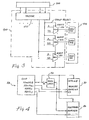
- the programmable pin designation for semiconductor devices 10 is comprised of a programming port 100, optional programming logic 200 (shown in dashed lines to indicate an optional, not a required, element), configuration logic 300, selection logic 400 and at least one pin 500, which may be programmably designated to perform one of a plurality of I/O functions.
- the system is further comprised of a plurality of semiconductor pins which are predesignated and unalterable, to perform a memory address function. These pins are shown in figure 4 as AD m :AD 0 , which is a diagram demonstrating several applications of the invention.
- the elements described above are co-located on a single, monolithic semiconductor device.
- the importance of the invention is to provide a semiconductor device such as a microcontroller, microprocessor or other devices capable of performing memory access with a flexible, programmable method of selecting the precise address range required for the application.
- the objective of the invention is to optimize the number of semiconductor pins needed for memory address functions and quasi-address functions such as chip select.
- the programming port 100 may be either a serial or parallel I/O port of various formats, standards and protocols which are well known to those skilled in the art.
- the programming port has several functions.
- the port 100 accepts semiconductor pin configuration data from a programming device that is beyond the scope of the invention, but is well known to those skilled in the art of computer science.
- the port 100 may also output the current configuration of the semiconductor pins to external devices. Also, the port 100 may be used for test purposes.
- the configuration data is transmitted via the programming port directly to the configuration logic 300 where it is stored.
- the configuration data is read by the programming logic 200, which may be a processing unit.
- the configuration data is interpreted by the programming logic 200.
- the interpreted form of the configuration data is stored in the configuration logic 300.
- the configuration logic 300 may include one of a number of implementations.
- the configuration logic 300 may be a simple register or a location within a programmable volatile or non-volatile memory array.
- the configuration data stored in the configuration logic may be modified at the discretion of the programmer.
- the configuration logic may encompass one time only programmable logic such as a programmable read only memory (PROM) or other types of fusible devices known to those skilled in the art.
- PROM programmable read only memory
- the selection logic 400 is shown.
- the selection logic provides the decision mechanism for designating semiconductor pin functions.
- the selection logic 400 is comprised of a series of multiplexers 410 in the preferred embodiment.
- the selection logic includes both the series of multiplexers 410 and one or more decoders 420.
- Figure 1 shows that the selection logic 400 provides the bridge between the data stored in the configuration logic 300 and the semiconductor pins 500.
- Figure 2 shows a non-encoded form of the selection logic 400 where there is one to one mapping between each bit of the configuration logic 300 and the select input for each multiplexer 410.
- Figure 3 shows an encoded form of the selection logic 400 where the configuration data is stored in an encoded format. The encoded data is then decoded by decode logic 420 and then coupled to the select inputs of the multiplexers 410.
- the inputs of the multiplexers 410 are either expanded address lines or other I/O functions performed by a semiconductor device.
- the outputs of the multiplexers 410 are connected to the semiconductor pins 500, either directly or through a buffer.
- the present invention 10 is embodied in block 20, which represents a processing unit such as a microprocessor or microcontroller.
- the application also illustrates memory device 30 and peripheral device 40.
- the address latch 50 is also illustrated.
- AD m :AD 0 in block 20 represents a predesignated set of pins with an address function.
- these pins may be coupled to the data bus in addition to driving the address bus.
- the predesignated set of address pins may not be multiplexed with the data bus function, thus obviating the requirement for the address latch 50.
- the predesignated nature of the address function of the semiconductor pins corresponding to AD m :AD 0 may not be altered or modified by the programmer.
- the memory device 30 and peripheral device 40 have addressable memory locations which exceed that provided for by the range defined by AD m :AD 0 . Therefore, addition memory addressing capability is required.
- the programmer defines the expanded addressing as A n :A m+1 , where n ⁇ m+1. This data is stored in the configuration logic 300 and the selection logic 400 determines the semiconductor pin 500 assignments (figures 1-3).
- Chip select logic is shown in block 20 as ADDR x and ADDR y .
- ADDR x and ADDR y By designating these pins as chip selects in the same manner as described above for expanded address pins, the appropriate memory/peripheral device is accessed.
- the present invention allows for flexible designation of IC pins for addressing, which precisely matches the addressing requirements of the design specification. Those pins not used for addressing are available for other I/O functions.
Landscapes
- Engineering & Computer Science (AREA)
- General Engineering & Computer Science (AREA)
- Physics & Mathematics (AREA)
- Computer Hardware Design (AREA)
- Mathematical Physics (AREA)
- Computing Systems (AREA)
- Theoretical Computer Science (AREA)
- General Physics & Mathematics (AREA)
- Logic Circuits (AREA)
- Microcomputers (AREA)
- Semiconductor Integrated Circuits (AREA)
- Design And Manufacture Of Integrated Circuits (AREA)
- Read Only Memory (AREA)
Claims (19)
- System zum in programmierbarer Weise Bestimmen von Halbleiterbauelementkontaktstiften mit in Kombination:einer Vielzahl von Kontaktstiften (Adm:AD0) mit einer vorbestimmten Adressfunktion;einem Programmierport (100) zum Empfang einer Vielzahl von Kontaktstiftbestimmungsbefehlen;einer mit dem Programmierport (100) gekoppelten Konfigurationslogik (300) zum Speichern der Vielzahl von Kontaktstiftbestimmungsbefehlen;einer mit der Konfigurationslogik (300) gekoppelten Auswahllogik (400) zum Auswählen der Funktion mindestens einer Kontaktstiftbestimmung; undmindestens einem Kontaktstift (500), der mit der Auswahllogik (400) gekoppelt ist und der in programmierbarer Weise dazu bestimmt ist, eine aus einer Vielzahl von E/A-Funktionen auszurühren.
- System nach Anspruch 1, das zudem eine mit dem Programmierport (100) verbundene Programmierlogik (200) zum Auswerten der Vielzahl von Kontaktstiftbestimmungsbefehlen aufweist.
- System nach Anspruch 2, bei dem der Programmierport (100), die Konfigurationslogik (300), die Auswahllogik (400), der mindestens eine Kontaktstift (500) und die Vielzahl von Kontaktstiften (Adm:AD0) mit der vorbestimmten Adressfunktion alle auf einem einzigen monolithischen Halbleiterbauelement angeordnet sind.
- System nach Anspruch 1, bei dem der Programmierport (100) für den Empfang einer Vielzahl von Kontaktstiftbestimmungsbefehlen ein serieller Port ist.
- System nach Anspruch 1, bei dem der Programmierport (100) für den Empfang einer Vielzahl von Kontaktstiftbestimmungsbefehlen ein paralleler Port ist.
- System nach Anspruch 1, bei dem die Konfigurationslogik (300) durch mindestens ein Register gegeben ist.
- System nach Anspruch 1, bei dem die Konfigurationslogik (300) durch eine abschmelzbare Vorrichtung gegeben ist.
- System nach Anspruch 1, bei dem die Konfigurationslogik durch einen nicht flüchtigen Speicher gegeben ist.
- System nach Anspruch 1, bei dem die Auswahllogik (400) durch mindestens einen Multiplexer gegeben ist.
- System nach Anspruch 1, bei dem der mindestens eine Kontaktstift (500) als ein Adressierpin bestimmt sein kann.
- System nach Anspruch 2, bei dem der mindestens eine Kontaktstift (500) bestimmt sein kann als ein Adresskontaktstift, der einen adressierbaren Speicherbereich über das hinaus erweitern kann, was durch die Vielzahl der Adresskontaktstifte (Adm:AD0) mit den vorbestimmten Adressfunktionen bereitgestellt wird.
- System nach Anspruch 1, bei dem der mindestens eine Kontaktstift (500) als ein Chipauswahlkontaktstift bestimmt werden kann.
- System nach Anspruch 1, bei dem der mindestens eine Kontaktstift (500) bestimmt sein kann als Chipauswahlkontaktstift, der zum Ausdehnen des adressierbaren Speicherbereichs über das hinaus, was durch die Vielzahl von Adresskontaktstiften (Adm:AD0) mit der vorbestimmten Adressfunktion bereitstellt.
- System nach Anspruch 2, bei dem die Programmierlogik (200) durch eine Prozessoreinheit gegeben ist, welche die Vielzahl von Kontaktstiftbestimmungsbefehlen auswertet und eine Vielzahl von Kontaktstiftbestimmungsanweisungen innerhalb der Konfigurationslogik (300) speichert.
- System nach Anspruch 13, bei dem die Vielzahl von Kontaktstiftbestimmungsanweisungen kodierte Anweisungen sind.
- System nach Anspruch 2, bei dem die Auswahllogik (400) durch mindestens einen Multiplexer gegeben ist.
- System nach Anspruch 15, bei dem die Auswahllogik (400) weiterhin durch eine Dekodierlogik zum Dekodieren der Vielzahl von Kontaktstiftbestimmungsanweisungen aufweist.
- Verfahren zum in programmierbarer Weise bestimmen von Halbleiterkontaktstiften mit den Schritten:Bereitstellen einer Vielzahl von Kontaktstiften (Adm:AD0) mit einer vorbestimmten Adressfunktion;Bereitstellen einer Vielzahl von Kontaktstiftbestimmungsbefehlen an einen Programmierport (100);Bereitstellen mindestens eines Konfigurationsregisters (300), um die Vielzahl von Kontaktstiftbestimmungsbefehlen zu speichern, die vom Programmierport (100) erhalten werden;Bereitstellen einer Auswahllogik (400), welche durch die in dem mindestens einen Konfigurationsregister (300) zum Auswählen einer aus einer Vielzahl von E/A-Funktionen gespeicherten Kontaktstiftbestimmungsbefehle gesteuert wird; undBereitstellen mindestens eines Kontaktstifts, der mit der Auswahllogik (400) gekoppelten ist und der in programmierbarer Weise dazu bestimmt, eine aus der Vielzahl von E/A-Funktionen durchzuführen.
- Verfahren nach Anspruch 18, zudem mit dem Schritt des Bereitstellens einer Programmierlogik (200), die mit dem Programmierport (100) zum Auswerten der Vielzahl von Kontaktstiftbestimmungsbefehlen gekoppelt ist.
Applications Claiming Priority (2)
| Application Number | Priority Date | Filing Date | Title |
|---|---|---|---|
| US09/085,826 US6057705A (en) | 1998-05-28 | 1998-05-28 | Programmable pin designation for semiconductor devices |
| US85826 | 1998-05-28 |
Publications (3)
| Publication Number | Publication Date |
|---|---|
| EP0967723A2 EP0967723A2 (de) | 1999-12-29 |
| EP0967723A3 EP0967723A3 (de) | 2000-08-23 |
| EP0967723B1 true EP0967723B1 (de) | 2003-09-24 |
Family
ID=22194199
Family Applications (1)
| Application Number | Title | Priority Date | Filing Date |
|---|---|---|---|
| EP98122505A Expired - Lifetime EP0967723B1 (de) | 1998-05-28 | 1998-11-27 | Programmierbare Pinbezeichnung für Halbleitervorrichtungen |
Country Status (7)
| Country | Link |
|---|---|
| US (1) | US6057705A (de) |
| EP (1) | EP0967723B1 (de) |
| JP (1) | JPH11353300A (de) |
| KR (1) | KR19990088601A (de) |
| CN (1) | CN1244069A (de) |
| AT (1) | ATE250827T1 (de) |
| DE (1) | DE69818434D1 (de) |
Families Citing this family (66)
| Publication number | Priority date | Publication date | Assignee | Title |
|---|---|---|---|---|
| US6515506B1 (en) * | 2000-05-03 | 2003-02-04 | Marvell International, Ltd. | Circuit for reducing pin count of a semiconductor chip and method for configuring the chip |
| US6606670B1 (en) * | 2000-08-16 | 2003-08-12 | Microchip Technology Incorporated | Circuit serial programming of default configuration |
| US6724220B1 (en) | 2000-10-26 | 2004-04-20 | Cyress Semiconductor Corporation | Programmable microcontroller architecture (mixed analog/digital) |
| US7765095B1 (en) | 2000-10-26 | 2010-07-27 | Cypress Semiconductor Corporation | Conditional branching in an in-circuit emulation system |
| US6981090B1 (en) * | 2000-10-26 | 2005-12-27 | Cypress Semiconductor Corporation | Multiple use of microcontroller pad |
| US6892310B1 (en) * | 2000-10-26 | 2005-05-10 | Cypress Semiconductor Corporation | Method for efficient supply of power to a microcontroller |
| US8160864B1 (en) | 2000-10-26 | 2012-04-17 | Cypress Semiconductor Corporation | In-circuit emulator and pod synchronized boot |
| US8103496B1 (en) | 2000-10-26 | 2012-01-24 | Cypress Semicondutor Corporation | Breakpoint control in an in-circuit emulation system |
| US8149048B1 (en) | 2000-10-26 | 2012-04-03 | Cypress Semiconductor Corporation | Apparatus and method for programmable power management in a programmable analog circuit block |
| US8176296B2 (en) | 2000-10-26 | 2012-05-08 | Cypress Semiconductor Corporation | Programmable microcontroller architecture |
| US6417689B1 (en) * | 2001-01-16 | 2002-07-09 | Xilinx, Inc. | Method and apparatus for placing output signals having different voltage levels on output pins of a programmable logic device |
| US20040015617A1 (en) * | 2001-01-25 | 2004-01-22 | Sangha Onkar S. | Flexible network interfaces and flexible data clocking |
| US6509758B2 (en) | 2001-04-18 | 2003-01-21 | Cygnal Integrated Products, Inc. | IC with digital and analog circuits and mixed signal I/O pins |
| US6507215B1 (en) | 2001-04-18 | 2003-01-14 | Cygnal Integrated Products, Inc. | Programmable driver for an I/O pin of an integrated circuit |
| US7406674B1 (en) | 2001-10-24 | 2008-07-29 | Cypress Semiconductor Corporation | Method and apparatus for generating microcontroller configuration information |
| US8078970B1 (en) | 2001-11-09 | 2011-12-13 | Cypress Semiconductor Corporation | Graphical user interface with user-selectable list-box |
| US8042093B1 (en) | 2001-11-15 | 2011-10-18 | Cypress Semiconductor Corporation | System providing automatic source code generation for personalization and parameterization of user modules |
| US8069405B1 (en) | 2001-11-19 | 2011-11-29 | Cypress Semiconductor Corporation | User interface for efficiently browsing an electronic document using data-driven tabs |
| US6971004B1 (en) | 2001-11-19 | 2005-11-29 | Cypress Semiconductor Corp. | System and method of dynamically reconfiguring a programmable integrated circuit |
| US7770113B1 (en) | 2001-11-19 | 2010-08-03 | Cypress Semiconductor Corporation | System and method for dynamically generating a configuration datasheet |
| US6701508B1 (en) * | 2001-11-19 | 2004-03-02 | Cypress Semiconductor Corporation | Method and system for using a graphics user interface for programming an electronic device |
| US7774190B1 (en) | 2001-11-19 | 2010-08-10 | Cypress Semiconductor Corporation | Sleep and stall in an in-circuit emulation system |
| US7844437B1 (en) | 2001-11-19 | 2010-11-30 | Cypress Semiconductor Corporation | System and method for performing next placements and pruning of disallowed placements for programming an integrated circuit |
| US6492853B1 (en) | 2001-12-13 | 2002-12-10 | Cypress Semiconductor Corp. | Master/slave method for a ZQ-circuitry in multiple die devices |
| US20030154331A1 (en) * | 2002-02-13 | 2003-08-14 | Globespanvirata Incorporated | System and method for shared use of common GPIO line |
| US8103497B1 (en) | 2002-03-28 | 2012-01-24 | Cypress Semiconductor Corporation | External interface for event architecture |
| US7308608B1 (en) | 2002-05-01 | 2007-12-11 | Cypress Semiconductor Corporation | Reconfigurable testing system and method |
| US7761845B1 (en) | 2002-09-09 | 2010-07-20 | Cypress Semiconductor Corporation | Method for parameterizing a user module |
| KR100596450B1 (ko) * | 2003-12-11 | 2006-07-03 | 삼성전자주식회사 | 동작모드에 따라 데이터 스트로브 타입을 선택적으로사용할 수 있는 반도체 메모리 장치 |
| JP4489454B2 (ja) * | 2004-02-16 | 2010-06-23 | 富士通マイクロエレクトロニクス株式会社 | 半導体集積回路 |
| US7295049B1 (en) | 2004-03-25 | 2007-11-13 | Cypress Semiconductor Corporation | Method and circuit for rapid alignment of signals |
| US7285980B2 (en) * | 2004-07-27 | 2007-10-23 | Stmicroelectronics Pvt. Ltd. | Method and apparatus for multiplexing an integrated circuit pin |
| US8286125B2 (en) | 2004-08-13 | 2012-10-09 | Cypress Semiconductor Corporation | Model for a hardware device-independent method of defining embedded firmware for programmable systems |
| US8069436B2 (en) | 2004-08-13 | 2011-11-29 | Cypress Semiconductor Corporation | Providing hardware independence to automate code generation of processing device firmware |
| US7248530B2 (en) * | 2004-10-29 | 2007-07-24 | Infineon Technologies, Ag | Integrated semiconductor memory device |
| US7332976B1 (en) * | 2005-02-04 | 2008-02-19 | Cypress Semiconductor Corporation | Poly-phase frequency synthesis oscillator |
| TWI266477B (en) * | 2005-03-29 | 2006-11-11 | Realtek Semiconductor Corp | Chip with adjustable pinout function and method thereof |
| US7400183B1 (en) | 2005-05-05 | 2008-07-15 | Cypress Semiconductor Corporation | Voltage controlled oscillator delay cell and method |
| US8089461B2 (en) | 2005-06-23 | 2012-01-03 | Cypress Semiconductor Corporation | Touch wake for electronic devices |
| US8085067B1 (en) | 2005-12-21 | 2011-12-27 | Cypress Semiconductor Corporation | Differential-to-single ended signal converter circuit and method |
| US8067948B2 (en) | 2006-03-27 | 2011-11-29 | Cypress Semiconductor Corporation | Input/output multiplexer bus |
| US7436207B2 (en) * | 2006-07-21 | 2008-10-14 | Microchip Technology Incorporated | Integrated circuit device having at least one of a plurality of bond pads with a selectable plurality of input-output functionalities |
| US7728619B1 (en) | 2007-03-30 | 2010-06-01 | Cypress Semiconductor Corporation | Circuit and method for cascading programmable impedance matching in a multi-chip system |
| US8040266B2 (en) * | 2007-04-17 | 2011-10-18 | Cypress Semiconductor Corporation | Programmable sigma-delta analog-to-digital converter |
| US8130025B2 (en) | 2007-04-17 | 2012-03-06 | Cypress Semiconductor Corporation | Numerical band gap |
| US8516025B2 (en) | 2007-04-17 | 2013-08-20 | Cypress Semiconductor Corporation | Clock driven dynamic datapath chaining |
| US8092083B2 (en) * | 2007-04-17 | 2012-01-10 | Cypress Semiconductor Corporation | Temperature sensor with digital bandgap |
| US8026739B2 (en) | 2007-04-17 | 2011-09-27 | Cypress Semiconductor Corporation | System level interconnect with programmable switching |
| US7737724B2 (en) | 2007-04-17 | 2010-06-15 | Cypress Semiconductor Corporation | Universal digital block interconnection and channel routing |
| US9564902B2 (en) | 2007-04-17 | 2017-02-07 | Cypress Semiconductor Corporation | Dynamically configurable and re-configurable data path |
| US8065653B1 (en) | 2007-04-25 | 2011-11-22 | Cypress Semiconductor Corporation | Configuration of programmable IC design elements |
| US8266575B1 (en) | 2007-04-25 | 2012-09-11 | Cypress Semiconductor Corporation | Systems and methods for dynamically reconfiguring a programmable system on a chip |
| US9720805B1 (en) | 2007-04-25 | 2017-08-01 | Cypress Semiconductor Corporation | System and method for controlling a target device |
| US8049569B1 (en) | 2007-09-05 | 2011-11-01 | Cypress Semiconductor Corporation | Circuit and method for improving the accuracy of a crystal-less oscillator having dual-frequency modes |
| US8327173B2 (en) * | 2007-12-17 | 2012-12-04 | Nvidia Corporation | Integrated circuit device core power down independent of peripheral device operation |
| US9088176B2 (en) * | 2007-12-17 | 2015-07-21 | Nvidia Corporation | Power management efficiency using DC-DC and linear regulators in conjunction |
| US8347251B2 (en) * | 2007-12-31 | 2013-01-01 | Sandisk Corporation | Integrated circuit and manufacturing process facilitating selective configuration for electromagnetic compatibility |
| US9423846B2 (en) | 2008-04-10 | 2016-08-23 | Nvidia Corporation | Powered ring to maintain IO state independent of the core of an integrated circuit device |
| US8762759B2 (en) * | 2008-04-10 | 2014-06-24 | Nvidia Corporation | Responding to interrupts while in a reduced power state |
| US8601254B1 (en) * | 2009-04-30 | 2013-12-03 | Cypress Semiconductor Corp. | Configurable reset pin for input/output port |
| US9448964B2 (en) | 2009-05-04 | 2016-09-20 | Cypress Semiconductor Corporation | Autonomous control in a programmable system |
| CN103186301A (zh) * | 2011-12-30 | 2013-07-03 | 宸鸿光电科技股份有限公司 | 触控感测装置及其可程序化控制器 |
| CN103279436A (zh) * | 2013-04-25 | 2013-09-04 | 深圳市芯海科技有限公司 | 芯片引脚功能的配置方法和芯片 |
| TWI597812B (zh) * | 2015-09-15 | 2017-09-01 | Raydium Semiconductor Corp | 驅動電路及接腳輸出順序編排方法 |
| WO2018161321A1 (zh) * | 2017-03-09 | 2018-09-13 | 深圳市大疆创新科技有限公司 | F通道控制方法及装置 |
| CN108874709B (zh) | 2017-05-11 | 2023-05-16 | 恩智浦美国有限公司 | 引脚分配电路 |
Family Cites Families (10)
| Publication number | Priority date | Publication date | Assignee | Title |
|---|---|---|---|---|
| US4495603A (en) * | 1980-07-31 | 1985-01-22 | Varshney Ramesh C | Test system for segmented memory |
| US4717912A (en) * | 1982-10-07 | 1988-01-05 | Advanced Micro Devices, Inc. | Apparatus for producing any one of a plurality of signals at a single output |
| US5233539A (en) * | 1989-08-15 | 1993-08-03 | Advanced Micro Devices, Inc. | Programmable gate array with improved interconnect structure, input/output structure and configurable logic block |
| US5473758A (en) * | 1992-08-31 | 1995-12-05 | Microchip Technology Incorporated | System having input output pins shifting between programming mode and normal mode to program memory without dedicating input output pins for programming mode |
| US5495422A (en) * | 1993-10-12 | 1996-02-27 | Wang Laboratories, Inc. | Method for combining a plurality of independently operating circuits within a single package |
| US5504439A (en) * | 1994-04-01 | 1996-04-02 | Xilinx, Inc. | I/O interface cell for use with optional pad |
| US5787299A (en) * | 1994-09-16 | 1998-07-28 | Philips Electronics North American Corporation | Pin selection system for microcontroller having multiplexer selects between address/data signals and special signals produced by special function device |
| US5594367A (en) * | 1995-10-16 | 1997-01-14 | Xilinx, Inc. | Output multiplexer within input/output circuit for time multiplexing and high speed logic |
| US5744980A (en) * | 1996-02-16 | 1998-04-28 | Actel Corporation | Flexible, high-performance static RAM architecture for field-programmable gate arrays |
| US5686844A (en) * | 1996-05-24 | 1997-11-11 | Microchip Technology Incorporated | Integrated circuit pins configurable as a clock input pin and as a digital I/O pin or as a device reset pin and as a digital I/O pin and method therefor |
-
1998
- 1998-05-28 US US09/085,826 patent/US6057705A/en not_active Expired - Lifetime
- 1998-11-27 EP EP98122505A patent/EP0967723B1/de not_active Expired - Lifetime
- 1998-11-27 DE DE69818434T patent/DE69818434D1/de not_active Expired - Lifetime
- 1998-11-27 AT AT98122505T patent/ATE250827T1/de not_active IP Right Cessation
-
1999
- 1999-01-11 JP JP471699A patent/JPH11353300A/ja not_active Withdrawn
- 1999-05-27 KR KR1019990019190A patent/KR19990088601A/ko not_active Withdrawn
- 1999-05-28 CN CN99107072A patent/CN1244069A/zh active Pending
Also Published As
| Publication number | Publication date |
|---|---|
| US6057705A (en) | 2000-05-02 |
| CN1244069A (zh) | 2000-02-09 |
| EP0967723A3 (de) | 2000-08-23 |
| DE69818434D1 (de) | 2003-10-30 |
| KR19990088601A (ko) | 1999-12-27 |
| ATE250827T1 (de) | 2003-10-15 |
| EP0967723A2 (de) | 1999-12-29 |
| JPH11353300A (ja) | 1999-12-24 |
Similar Documents
| Publication | Publication Date | Title |
|---|---|---|
| EP0967723B1 (de) | Programmierbare Pinbezeichnung für Halbleitervorrichtungen | |
| EP0840455B1 (de) | Durch einen Mikrokontroller steuerbare Makrozelle | |
| EP0840953A1 (de) | Konfigurierbare ic-ausgangsklemmen | |
| KR20090009904A (ko) | 어드레스 식별자 코드 기입 방법 및 시스템, 및 i2c 가능디바이스 | |
| US6483183B1 (en) | Integrated circuit (IC) package with a microcontroller having an n-bit bus and up to n-pins coupled to the microcontroller | |
| US10971237B2 (en) | Semiconductor device | |
| JPH11203204A (ja) | 読出しおよび/または書込み保護可能領域を含む電気的に消去再書込み可能な不揮発性メモリ、ならびにこのメモリを内蔵した電子システム | |
| US6212591B1 (en) | Configurable I/O circuitry defining virtual ports | |
| US6894914B2 (en) | Nonvolatile memory device with parallel and serial functioning mode and selectable communication protocol | |
| EP0488678A2 (de) | Programmierbare integrierte Schaltung | |
| US5821772A (en) | Programmable address decoder for programmable logic device | |
| US5999991A (en) | Programmably selectable addresses for expansion cards for a motherboard | |
| CA2266259A1 (en) | Variable length register device | |
| US5781796A (en) | System for automatic configuration of I/O base address without configuration program using readout data on common bus by responding device | |
| JP2003044303A (ja) | コンピュータ装置 | |
| US6912173B2 (en) | Method and system for fast memory access | |
| KR940002477B1 (ko) | 마이크로제어기를 이용한 다목적 제어 시스템 | |
| KR20030085046A (ko) | 동기 비휘발성 메모리 소자용 독립 비동기 부트 블록 | |
| EP1367598A1 (de) | Testverfahren und Anordnung für nichtflüchtige Speicher mit einer über nur wenige Anschlusskontakte verfügenden seriellen Kommunikations-Schnittstelle | |
| KR100265550B1 (ko) | 버스제어기를갖는데이타프로세서 | |
| US7185117B2 (en) | Microcomputer and evaluation device, evaluation method thereof | |
| JP4319142B2 (ja) | 識別コード組込み型集積回路 | |
| JP2970225B2 (ja) | 入出力回路 | |
| US6385717B1 (en) | Programmable 1-bit data processing arrangement | |
| JP3491838B2 (ja) | 入出力拡張システム |
Legal Events
| Date | Code | Title | Description |
|---|---|---|---|
| PUAI | Public reference made under article 153(3) epc to a published international application that has entered the european phase |
Free format text: ORIGINAL CODE: 0009012 |
|
| AK | Designated contracting states |
Kind code of ref document: A2 Designated state(s): AT BE CH DE ES FR GB IT LI NL SE |
|
| AX | Request for extension of the european patent |
Free format text: AL;LT;LV;MK;RO;SI |
|
| 17P | Request for examination filed |
Effective date: 20000313 |
|
| PUAL | Search report despatched |
Free format text: ORIGINAL CODE: 0009013 |
|
| AK | Designated contracting states |
Kind code of ref document: A3 Designated state(s): AT BE CH CY DE DK ES FI FR GB GR IE IT LI LU MC NL PT SE |
|
| AX | Request for extension of the european patent |
Free format text: AL;LT;LV;MK;RO;SI |
|
| RIC1 | Information provided on ipc code assigned before grant |
Free format text: 7H 03K 19/173 A, 7G 06F 1/22 B, 7G 06F 12/06 B |
|
| AKX | Designation fees paid |
Free format text: AT BE CH DE ES FR GB IT LI NL SE |
|
| 17Q | First examination report despatched |
Effective date: 20010717 |
|
| GRAG | Despatch of communication of intention to grant |
Free format text: ORIGINAL CODE: EPIDOS AGRA |
|
| GRAG | Despatch of communication of intention to grant |
Free format text: ORIGINAL CODE: EPIDOS AGRA |
|
| GRAH | Despatch of communication of intention to grant a patent |
Free format text: ORIGINAL CODE: EPIDOS IGRA |
|
| GRAH | Despatch of communication of intention to grant a patent |
Free format text: ORIGINAL CODE: EPIDOS IGRA |
|
| GRAA | (expected) grant |
Free format text: ORIGINAL CODE: 0009210 |
|
| AK | Designated contracting states |
Kind code of ref document: B1 Designated state(s): AT BE CH DE ES FR GB IT LI NL SE |
|
| PG25 | Lapsed in a contracting state [announced via postgrant information from national office to epo] |
Ref country code: NL Free format text: LAPSE BECAUSE OF FAILURE TO SUBMIT A TRANSLATION OF THE DESCRIPTION OR TO PAY THE FEE WITHIN THE PRESCRIBED TIME-LIMIT Effective date: 20030924 Ref country code: LI Free format text: LAPSE BECAUSE OF FAILURE TO SUBMIT A TRANSLATION OF THE DESCRIPTION OR TO PAY THE FEE WITHIN THE PRESCRIBED TIME-LIMIT Effective date: 20030924 Ref country code: IT Free format text: LAPSE BECAUSE OF FAILURE TO SUBMIT A TRANSLATION OF THE DESCRIPTION OR TO PAY THE FEE WITHIN THE PRE;WARNING: LAPSES OF ITALIAN PATENTS WITH EFFECTIVE DATE BEFORE 2007 MAY HAVE OCCURRED AT ANY TIME BEFORE 2007. THE CORRECT EFFECTIVE DATE MAY BE DIFFERENT FROM THE ONE RECORDED.SCRIBED TIME-LIMIT Effective date: 20030924 Ref country code: FR Free format text: LAPSE BECAUSE OF FAILURE TO SUBMIT A TRANSLATION OF THE DESCRIPTION OR TO PAY THE FEE WITHIN THE PRESCRIBED TIME-LIMIT Effective date: 20030924 Ref country code: CH Free format text: LAPSE BECAUSE OF FAILURE TO SUBMIT A TRANSLATION OF THE DESCRIPTION OR TO PAY THE FEE WITHIN THE PRESCRIBED TIME-LIMIT Effective date: 20030924 Ref country code: BE Free format text: LAPSE BECAUSE OF FAILURE TO SUBMIT A TRANSLATION OF THE DESCRIPTION OR TO PAY THE FEE WITHIN THE PRESCRIBED TIME-LIMIT Effective date: 20030924 Ref country code: AT Free format text: LAPSE BECAUSE OF FAILURE TO SUBMIT A TRANSLATION OF THE DESCRIPTION OR TO PAY THE FEE WITHIN THE PRESCRIBED TIME-LIMIT Effective date: 20030924 |
|
| REG | Reference to a national code |
Ref country code: GB Ref legal event code: FG4D |
|
| REG | Reference to a national code |
Ref country code: CH Ref legal event code: EP |
|
| REF | Corresponds to: |
Ref document number: 69818434 Country of ref document: DE Date of ref document: 20031030 Kind code of ref document: P |
|
| PG25 | Lapsed in a contracting state [announced via postgrant information from national office to epo] |
Ref country code: SE Free format text: LAPSE BECAUSE OF FAILURE TO SUBMIT A TRANSLATION OF THE DESCRIPTION OR TO PAY THE FEE WITHIN THE PRESCRIBED TIME-LIMIT Effective date: 20031224 Ref country code: GB Free format text: LAPSE BECAUSE OF NON-PAYMENT OF DUE FEES Effective date: 20031224 |
|
| PG25 | Lapsed in a contracting state [announced via postgrant information from national office to epo] |
Ref country code: DE Free format text: LAPSE BECAUSE OF FAILURE TO SUBMIT A TRANSLATION OF THE DESCRIPTION OR TO PAY THE FEE WITHIN THE PRESCRIBED TIME-LIMIT Effective date: 20031225 |
|
| PG25 | Lapsed in a contracting state [announced via postgrant information from national office to epo] |
Ref country code: ES Free format text: LAPSE BECAUSE OF FAILURE TO SUBMIT A TRANSLATION OF THE DESCRIPTION OR TO PAY THE FEE WITHIN THE PRESCRIBED TIME-LIMIT Effective date: 20040104 |
|
| NLV1 | Nl: lapsed or annulled due to failure to fulfill the requirements of art. 29p and 29m of the patents act | ||
| REG | Reference to a national code |
Ref country code: CH Ref legal event code: PL |
|
| PLBE | No opposition filed within time limit |
Free format text: ORIGINAL CODE: 0009261 |
|
| STAA | Information on the status of an ep patent application or granted ep patent |
Free format text: STATUS: NO OPPOSITION FILED WITHIN TIME LIMIT |
|
| GBPC | Gb: european patent ceased through non-payment of renewal fee |
Effective date: 20031224 |
|
| 26N | No opposition filed |
Effective date: 20040625 |
|
| EN | Fr: translation not filed |