EP0968507B1 - Cellule photovaltaique - Google Patents
Cellule photovaltaique Download PDFInfo
- Publication number
- EP0968507B1 EP0968507B1 EP98913727A EP98913727A EP0968507B1 EP 0968507 B1 EP0968507 B1 EP 0968507B1 EP 98913727 A EP98913727 A EP 98913727A EP 98913727 A EP98913727 A EP 98913727A EP 0968507 B1 EP0968507 B1 EP 0968507B1
- Authority
- EP
- European Patent Office
- Prior art keywords
- group
- cell
- naphthyl
- accordance
- several
- Prior art date
- Legal status (The legal status is an assumption and is not a legal conclusion. Google has not performed a legal analysis and makes no representation as to the accuracy of the status listed.)
- Expired - Lifetime
Links
Images

Classifications
-
- H—ELECTRICITY
- H10—SEMICONDUCTOR DEVICES; ELECTRIC SOLID-STATE DEVICES NOT OTHERWISE PROVIDED FOR
- H10K—ORGANIC ELECTRIC SOLID-STATE DEVICES
- H10K85/00—Organic materials used in the body or electrodes of devices covered by this subclass
- H10K85/60—Organic compounds having low molecular weight
- H10K85/631—Amine compounds having at least two aryl rest on at least one amine-nitrogen atom, e.g. triphenylamine
-
- H—ELECTRICITY
- H10—SEMICONDUCTOR DEVICES; ELECTRIC SOLID-STATE DEVICES NOT OTHERWISE PROVIDED FOR
- H10K—ORGANIC ELECTRIC SOLID-STATE DEVICES
- H10K85/00—Organic materials used in the body or electrodes of devices covered by this subclass
- H10K85/40—Organosilicon compounds, e.g. TIPS pentacene
-
- H—ELECTRICITY
- H10—SEMICONDUCTOR DEVICES; ELECTRIC SOLID-STATE DEVICES NOT OTHERWISE PROVIDED FOR
- H10K—ORGANIC ELECTRIC SOLID-STATE DEVICES
- H10K85/00—Organic materials used in the body or electrodes of devices covered by this subclass
- H10K85/60—Organic compounds having low molecular weight
- H10K85/615—Polycyclic condensed aromatic hydrocarbons, e.g. anthracene
- H10K85/626—Polycyclic condensed aromatic hydrocarbons, e.g. anthracene containing more than one polycyclic condensed aromatic rings, e.g. bis-anthracene
-
- H—ELECTRICITY
- H10—SEMICONDUCTOR DEVICES; ELECTRIC SOLID-STATE DEVICES NOT OTHERWISE PROVIDED FOR
- H10K—ORGANIC ELECTRIC SOLID-STATE DEVICES
- H10K2102/00—Constructional details relating to the organic devices covered by this subclass
- H10K2102/10—Transparent electrodes, e.g. using graphene
- H10K2102/101—Transparent electrodes, e.g. using graphene comprising transparent conductive oxides [TCO]
- H10K2102/102—Transparent electrodes, e.g. using graphene comprising transparent conductive oxides [TCO] comprising tin oxides, e.g. fluorine-doped SnO2
-
- H—ELECTRICITY
- H10—SEMICONDUCTOR DEVICES; ELECTRIC SOLID-STATE DEVICES NOT OTHERWISE PROVIDED FOR
- H10K—ORGANIC ELECTRIC SOLID-STATE DEVICES
- H10K30/00—Organic devices sensitive to infrared radiation, light, electromagnetic radiation of shorter wavelength or corpuscular radiation
- H10K30/10—Organic devices sensitive to infrared radiation, light, electromagnetic radiation of shorter wavelength or corpuscular radiation comprising heterojunctions between organic semiconductors and inorganic semiconductors
- H10K30/15—Sensitised wide-bandgap semiconductor devices, e.g. dye-sensitised TiO2
- H10K30/151—Sensitised wide-bandgap semiconductor devices, e.g. dye-sensitised TiO2 the wide bandgap semiconductor comprising titanium oxide, e.g. TiO2
-
- H—ELECTRICITY
- H10—SEMICONDUCTOR DEVICES; ELECTRIC SOLID-STATE DEVICES NOT OTHERWISE PROVIDED FOR
- H10K—ORGANIC ELECTRIC SOLID-STATE DEVICES
- H10K30/00—Organic devices sensitive to infrared radiation, light, electromagnetic radiation of shorter wavelength or corpuscular radiation
- H10K30/50—Photovoltaic [PV] devices
-
- H—ELECTRICITY
- H10—SEMICONDUCTOR DEVICES; ELECTRIC SOLID-STATE DEVICES NOT OTHERWISE PROVIDED FOR
- H10K—ORGANIC ELECTRIC SOLID-STATE DEVICES
- H10K85/00—Organic materials used in the body or electrodes of devices covered by this subclass
- H10K85/30—Coordination compounds
- H10K85/321—Metal complexes comprising a group IIIA element, e.g. Tris (8-hydroxyquinoline) gallium [Gaq3]
- H10K85/322—Metal complexes comprising a group IIIA element, e.g. Tris (8-hydroxyquinoline) gallium [Gaq3] comprising boron
-
- H—ELECTRICITY
- H10—SEMICONDUCTOR DEVICES; ELECTRIC SOLID-STATE DEVICES NOT OTHERWISE PROVIDED FOR
- H10K—ORGANIC ELECTRIC SOLID-STATE DEVICES
- H10K85/00—Organic materials used in the body or electrodes of devices covered by this subclass
- H10K85/30—Coordination compounds
- H10K85/341—Transition metal complexes, e.g. Ru(II)polypyridine complexes
- H10K85/344—Transition metal complexes, e.g. Ru(II)polypyridine complexes comprising ruthenium
-
- H—ELECTRICITY
- H10—SEMICONDUCTOR DEVICES; ELECTRIC SOLID-STATE DEVICES NOT OTHERWISE PROVIDED FOR
- H10K—ORGANIC ELECTRIC SOLID-STATE DEVICES
- H10K85/00—Organic materials used in the body or electrodes of devices covered by this subclass
- H10K85/60—Organic compounds having low molecular weight
- H10K85/615—Polycyclic condensed aromatic hydrocarbons, e.g. anthracene
- H10K85/622—Polycyclic condensed aromatic hydrocarbons, e.g. anthracene containing four rings, e.g. pyrene
-
- H—ELECTRICITY
- H10—SEMICONDUCTOR DEVICES; ELECTRIC SOLID-STATE DEVICES NOT OTHERWISE PROVIDED FOR
- H10K—ORGANIC ELECTRIC SOLID-STATE DEVICES
- H10K85/00—Organic materials used in the body or electrodes of devices covered by this subclass
- H10K85/60—Organic compounds having low molecular weight
- H10K85/615—Polycyclic condensed aromatic hydrocarbons, e.g. anthracene
- H10K85/623—Polycyclic condensed aromatic hydrocarbons, e.g. anthracene containing five rings, e.g. pentacene
-
- H—ELECTRICITY
- H10—SEMICONDUCTOR DEVICES; ELECTRIC SOLID-STATE DEVICES NOT OTHERWISE PROVIDED FOR
- H10K—ORGANIC ELECTRIC SOLID-STATE DEVICES
- H10K85/00—Organic materials used in the body or electrodes of devices covered by this subclass
- H10K85/60—Organic compounds having low molecular weight
- H10K85/631—Amine compounds having at least two aryl rest on at least one amine-nitrogen atom, e.g. triphenylamine
- H10K85/633—Amine compounds having at least two aryl rest on at least one amine-nitrogen atom, e.g. triphenylamine comprising polycyclic condensed aromatic hydrocarbons as substituents on the nitrogen atom
-
- H—ELECTRICITY
- H10—SEMICONDUCTOR DEVICES; ELECTRIC SOLID-STATE DEVICES NOT OTHERWISE PROVIDED FOR
- H10K—ORGANIC ELECTRIC SOLID-STATE DEVICES
- H10K85/00—Organic materials used in the body or electrodes of devices covered by this subclass
- H10K85/60—Organic compounds having low molecular weight
- H10K85/649—Aromatic compounds comprising a hetero atom
- H10K85/652—Cyanine dyes
-
- H—ELECTRICITY
- H10—SEMICONDUCTOR DEVICES; ELECTRIC SOLID-STATE DEVICES NOT OTHERWISE PROVIDED FOR
- H10K—ORGANIC ELECTRIC SOLID-STATE DEVICES
- H10K85/00—Organic materials used in the body or electrodes of devices covered by this subclass
- H10K85/60—Organic compounds having low molecular weight
- H10K85/649—Aromatic compounds comprising a hetero atom
- H10K85/656—Aromatic compounds comprising a hetero atom comprising two or more different heteroatoms per ring
- H10K85/6565—Oxadiazole compounds
-
- H—ELECTRICITY
- H10—SEMICONDUCTOR DEVICES; ELECTRIC SOLID-STATE DEVICES NOT OTHERWISE PROVIDED FOR
- H10K—ORGANIC ELECTRIC SOLID-STATE DEVICES
- H10K85/00—Organic materials used in the body or electrodes of devices covered by this subclass
- H10K85/60—Organic compounds having low molecular weight
- H10K85/649—Aromatic compounds comprising a hetero atom
- H10K85/657—Polycyclic condensed heteroaromatic hydrocarbons
- H10K85/6572—Polycyclic condensed heteroaromatic hydrocarbons comprising only nitrogen in the heteroaromatic polycondensed ring system, e.g. phenanthroline or carbazole
-
- Y—GENERAL TAGGING OF NEW TECHNOLOGICAL DEVELOPMENTS; GENERAL TAGGING OF CROSS-SECTIONAL TECHNOLOGIES SPANNING OVER SEVERAL SECTIONS OF THE IPC; TECHNICAL SUBJECTS COVERED BY FORMER USPC CROSS-REFERENCE ART COLLECTIONS [XRACs] AND DIGESTS
- Y02—TECHNOLOGIES OR APPLICATIONS FOR MITIGATION OR ADAPTATION AGAINST CLIMATE CHANGE
- Y02E—REDUCTION OF GREENHOUSE GAS [GHG] EMISSIONS, RELATED TO ENERGY GENERATION, TRANSMISSION OR DISTRIBUTION
- Y02E10/00—Energy generation through renewable energy sources
- Y02E10/50—Photovoltaic [PV] energy
- Y02E10/549—Organic PV cells
-
- Y—GENERAL TAGGING OF NEW TECHNOLOGICAL DEVELOPMENTS; GENERAL TAGGING OF CROSS-SECTIONAL TECHNOLOGIES SPANNING OVER SEVERAL SECTIONS OF THE IPC; TECHNICAL SUBJECTS COVERED BY FORMER USPC CROSS-REFERENCE ART COLLECTIONS [XRACs] AND DIGESTS
- Y02—TECHNOLOGIES OR APPLICATIONS FOR MITIGATION OR ADAPTATION AGAINST CLIMATE CHANGE
- Y02P—CLIMATE CHANGE MITIGATION TECHNOLOGIES IN THE PRODUCTION OR PROCESSING OF GOODS
- Y02P70/00—Climate change mitigation technologies in the production process for final industrial or consumer products
- Y02P70/50—Manufacturing or production processes characterised by the final manufactured product
Definitions
- a photovoltaic cell is a component in which light is converted directly into electrical energy. In addition to two electrodes, it contains at least one light-absorbing layer and one charge transport layer. If it is sunlight, one speaks of a solar cell. Although Becquerel had already observed the photovoltaic effect, i.e. the appearance of a voltage across a pn junction when exposed to light, in 1893, it was only with the development of semiconductor technology in the 1940s and 1950s that the first functional solar cells were produced. Since the voltage of a single solar cell is generally low (typically ⁇ 1V), cells are usually connected in series to form so-called modules.
- the solar cells used today usually contain a semiconductor material as the light-absorbing layer, in most cases silicon, which, however, must meet the highest demands on the purity and quality of processing for this application. As a result, solar cells today are not competitive in many applications for cost reasons.
- a dye-sensitized solar cell as developed by H. Tributsch in the 1960s, uses a material with a very large band gap, such as titanium dioxide, as a semiconductor.
- a dye chromophore
- the semiconductor is mainly used to transport electrons. No special purity and perfection of the material is necessary for this.
- the semiconductor layer can e.g. B. can be simply painted from a powder suspension onto conductive glass.
- a photovoltaic cell which has a charge transport layer containing a hole conductor material.
- EP-A 0 333 641 describes a photoelectrochemical cell which is characterized in that it contains a nanoporous metal oxide semiconductor, ie an extremely roughened and thus enlarged surface.
- the charge transport between the semiconductor / chromophore layer and the counter electrode takes place in this cell using an electrolyte solution.
- electrolyte solution Although good results are achieved with such cells, the property profile of such a device can still be clearly improved.
- the electron is returned to the dye by the diffusion of ions. As a result, only redox systems that are small enough to penetrate the pores of the nanocrystalline semiconductor layer come into question.
- the invention therefore relates to a photovoltaic cell according to claim 1 and to a use with the features of claim 13.
- the redox system preferably consists of one or more hole conductor connections.
- a semiconductor 12 which preferably has a surface with a roughness factor> 1, is applied as a light-absorbing layer on a conductive carrier 11, which can serve as an electrode or contact and consists, for example, of a metal or indium tin oxide (ITO).
- the cell according to the invention preferably contains a chromophore on the surface of the semiconductor, shown here as chromophore layer 13.
- the term light-absorbing layer encompasses both a semiconductor layer and a combination of semiconductor / chromophore, even if the actual absorption in this case takes place almost exclusively by the chromophore.
- the electrolyte 14 which according to the invention contains a hole conductor connection of the formula (I). It is delimited on one side by a counterelectrode 15, which can consist, for example, of a conductive glass, conductively coated plastic, metal or another conductive, preferably translucent material.
- Cell 1 is sealed at the top and bottom by an insulating layer 16 and 17, respectively. It can contain a side closure, not shown in the figure, for example a frame made of an electrically insulating material, such as plastic or glass. At least one side of the cell must be transparent to the light to be converted into electrical energy, so that it can reach the chromophore or the semiconductor.
- the cell according to the invention also contains not shown in the figure Devices for removing the electrical current generated by the cell.
- a hole conductor in the sense of the invention is a material that has a positive charge which can be caused by the absence of an electron, whereby Mass transport and charge transport are decoupled in the solid state.
- the cell used according to the invention lies in the cell according to the invention Hole conductor material of formula (I) dissolved in the electrolyte liquid before, and the charge transport takes place through the diffusion of the neutral or oxidized forms of the hole conductor.
- electron-rich, preferably organic compounds are suitable, which are oxidizable, preferably reversible. It is generally believed that the charge transport in an organic hole conductor material via the formation of Radical cations occur.
- the oxidation potential is variable over a wide range and can be attributed to specific energy levels of the semiconductor or sensitizer can be adjusted.
- the first oxidation potential is preferably between the energy level of the Ground state and 700, preferably 400, particularly preferably 300, mV above the ground state.
- Solvents are soluble.
- organic solvents but to which Invention is not limited to chloroform, benzene, chlorobenzene, Cyclohexanone, toluene, tetrahydrofuran, anisole, cresol, xylene, methyl lactate, Methylene chloride, hexane, nitrile compounds, or other aliphatic, aromatic or alcoholic solvents, including fully or partially fluorinated forms are preferred. It is sufficient for the production of an invention Hole conductor layer if the hole conductor material is in a corresponding Solvent is soluble. Soluble in the sense of the invention means one Solubility of at least 1.0 g / l at 25 ° C in an organic or inorganic solvents, preferably in one of the above Solvent.
- Hole conductor materials based on their size are also particularly preferred can diffuse into the pores of a rough semiconductor layer.
- hole conductor connections used as a redox system a molecular dimension comparable to that, if necessary used, molecules of the sensitizer (chromophore) so that the Molecules in close contact with those in the pores of the semiconductor surface Sensitizer molecules can come.
- Those are particularly preferred Hole conductor molecules less than a factor of 20, very particularly preferably 10, larger as corresponding sensitizer molecules.
- organic hole conductors examples include Triphenylmethanes, carbazoles, and N, N'-diphenyl-N, N'-bis (3-methylphenyl) - (1,1'-biphenyl) -4,4'-diamines (TPD).
- Spiro compounds are compounds in which two ring systems are linked by a single, four-bonded atom. This atom is called spiro atom, as in the Handbook of Chemistry and Physics 62 nd ed. (1981-2), CRC Press, pp C-23 to C-25 is executed.
- spiro compound means monomeric and polymeric carbospiro and heterospiro compounds.
- Preferred compounds of the formula (I) are 9,9'-spirobifluorene derivatives of the formula (II), where ⁇ has the meanings given above and where the benzo groups can be independently substituted and / or fused.
- the spiro compounds used according to the invention are produced according to methods known per se from the literature, such as those used in standard works on the organic Synthesis, e.g. Houben-Weyl, Methods of Organic Chemistry, Georg-Thieme-Verlag, Stuttgart and in the corresponding volumes of the series "The Chemistry of Heterocyclic Compounds "by A. Weissberger and E.C. Taylor (Editor) to be discribed.
- the preparation of compounds of the formula (IVa) can, for example, start from from tetrahalogenation in positions 2,2 ', 7,7' of 9,9'-spirobifluorene and subsequent substitution reaction take place (see e.g. US 5,026,894) or via a tetraacetylation of positions 2,2 ', 7,7' of 9,9'-spirobifluorene with subsequent C-C linkage after conversion of the acetyl groups to Aldehyde groups or heterocycle structure after conversion of the acetyl groups into Carboxylic acid groups take place.
- the preparation of compounds of the formula (IVb) can, for example, be analogous to those of the formula (IVa) take place, the stoichiometric ratios in the Implementation should be chosen so that the positions 2.2 'and 7.7' functionalized (see e.g. J.H. Weisburger, E.K. Weisburger, F.E. Ray, J. Am. Chem. Soc. 1959, 72 4253; F.K. Sutcliffe, H.M. Shahidi, D. Paterson, J. Soc. Dyers Color 1978, 94, 306 and G. Haas, V. Prelog, Helv. Chim. Acta 1969, 52 1202).
- the preparation of compounds of the formula (IVc) can be carried out, for example, via a Dibromination in the 2.2 'position and subsequent diacetylation in the 7.7' position of the 9,9'-spirobifluorene with subsequent reaction analogous to the compounds (IVa).
- disubstituted pyridines disubstituted pyrazines, disubstituted Pyrimidines and disubstituted pyridazines are found, for example, in corresponding volumes of the series "The Chemistry of Heterocyclic Compounds" by A. Weissberger and E. C. Taylor (editors).
- Heterospiro compounds of the formula (IIIa) can be prepared, for example, from a tetrahalogenation in positions 2,2 ', 7,7' of 9,9'-spirobi-9-silafluorene and subsequent substitution reaction, which is known from analogous C-spiro compounds (see, for example, US Pat. No. 5,026,894) or via a tetraacetylation of positions 2,2 ', 7,7' of 9,9'-spirobi-9-silafluorene with subsequent CC linkage after conversion of the acetyl groups into aldehyde groups or heterocycle formation after conversion of the acetyl groups into Carboxylic acid groups take place.
- the hole conductor material of formula (I) dissolved in the electrolyte liquid serves in one photovoltaic cell according to the invention due to its redox potential as pure relay substance for charge transport.
- the dye molecule becomes the basic state of the semiconductor or sensitizer dye regenerated.
- Another electron transfer takes place at the counter electrode the ground state of this molecule from the electrode to the hole conductor molecule regenerated.
- Solvents with a lower viscosity are desired Viscosity and low vapor pressure; in practice you want a compromise between viscosity and vapor pressure.
- the solvent should also have a Potential range of 3.0 V, namely at least from +1.5 V to -1.5 V, measured against an aqueous saturated calomel electrode, stable against redox reactions his. Solvents whose anodic limit potentials are still preferred are more positive. Solvents whose anodic are particularly preferred Limit potential is equal to or above 2.5 V.
- Suitable solvents which in no way limit the invention are acetonitrile, glutarodinitrile, Ethylene carbonate, propylene carbonate, chlorobenzene and 3-methyl-2-oxazilidinone as well their mixtures with one another or with other solvents.
- concentration of the oxidized form is preferably 0.001 - 0.2 M, particularly preferably 0.02 - 0.1 M
- the photovoltaic cell according to the invention contains a light-absorbing layer preferably a semiconductor that preferably has a very large band gap, particularly preferably at least 3.0 eV, particularly preferably above 3.0 eV, having.
- Metal oxide semiconductors in particular the oxides of the transition metals, and the elements of the third main group and the fourth, fifth and sixth subgroup (of the periodic system of the elements) of titanium, zirconium, hafnium, strontium, zinc, indium, yttrium, are therefore preferably suitable.
- perovskites such as SrTiO 3 , CaTiO 3
- oxides of other metals of the second and third main group or mixed oxides or oxide mixtures of these metals can also be used.
- Titanium dioxide is particularly preferred as the semiconductor material.
- the semiconductor preferably has a roughness factor of greater than 1, particularly preferably greater than 20, very particularly greater than 150.
- the roughness factor is defined as the ratio of a real / effective one Surface to the surface of the projection of this surface of a body, in this Case of the surface of the semiconductor.
- the roughness factor can be determined, for example, by gravimetric adsorption methods, such as, for example, in F. Kohlrausch, Practical Physics, Volume 1, P. 397 (Stuttgart: BG Teubner, 1985).
- the size of the pores is 5-200 nm, preferably 10-50 nm.
- a method for producing polycrystalline metal oxide semiconductor layers using the Sol-Gef method (described in detail, for example, in Stalder and Augustynski, J. Electrochem. Soc. 1979, 126, 2007), where in the method step the hydrolysis of the metal Alcoholate, the percentage relative humidity of the ambient atmosphere can be in a range from 30% to 80% and is kept constant within ⁇ 5%, preferably ⁇ 1%, results in metal oxide semiconductor layers with which a particularly high electrical yield is achieved in photovoltaic cells according to the invention can be achieved.
- the rough surface with a polycrystalline structure offers an area which is larger by the roughness factor for a, preferably, monomolecular surface layer of the chromophore.
- the semiconductor can be considered transparent to the incident luminous flux.
- light is partially reflected on the surface and reaches e.g. T. on neighboring surfaces.
- the penetrating into the semiconductor and not absorbed or converted light hits z. T. directly and partly indirectly and partly indirectly after total reflection on the surface, on the exit side on chromophore molecules, which makes it possible to achieve a significantly higher luminous efficiency.
- titanium oxide layer TiO 2
- the sol-gel process is described below as an example.
- the titanium substrate of pure titanium of about 99.5% purity is first cleaned in about 18% boiling HCl for about 30 minutes.
- the titanium ethoxide solution can e.g. B. be obtained by the solution of 21 mmol of TiCl 4 in 10 ml of very pure ethanol (puriss.). This solution is then diluted with very pure methanol (puriss.) To obtain a titanium concentration in the range of about 25 to 50 mg / ml.
- a drop of the solution is added to the titanium substrate and the titanium alkoxide is hydrolyzed at room temperature for about 30 minutes at a humidity of 48 ⁇ 1%.
- the substrate with the hydrolyzed layer is then heated to about 450 ° C. for about 15 minutes. This process is repeated several times. After repeating 10 to 15 times, the TiO 2 layer has reached a thickness of approximately 20 ⁇ m.
- the substrate with the layer is then baked at about 500 ° C. for about 30 minutes in a pure argon atmosphere (for example, 99.997%).
- the TiO 2 layer produced in this way has a roughness factor in the range of 200.
- Metal oxide semiconductor layers of this type can be produced on other substrates using analog processes.
- the upper layers of the semiconductor can optionally, such as. B. described in WO-A 91/16719, doped with a divalent or trivalent metal.
- the sensitivity that is to say the photoelectronic yield for visible light, that is to say also for sunlight, can be increased by so-called chromophores, also known as sensitizers or dyes, being chemically attached or incorporated (chemisorbed) as charge carriers on the surface of the semiconductor.
- chromophores also known as sensitizers or dyes
- the two functions of light absorption and charge carrier separation are separated in these photoelectronic systems.
- the light absorption is taken over by the chromophore in the surface area, and the charge carriers are separated at the semiconductor / chromophore interface.
- Different chromophores have different spectral sensitivities. The choice of the chromophore can thus be adapted to the spectral composition of the light from the light source in order to increase the yield as much as possible.
- the complexes of transition metals of the type metal (L 3 ), metal (L 2 ) of ruthenium and osmium are particularly suitable as chromophores, ie sensitizers '-dicarboxylic acid) and their salts, ruthenium cis diaqua bipyridyl complexes, such as ruthenium cis-diaqua bis (2,2'bipyridyl-4,4'dicarboxylate) and porphyrins (e.g. zinc tetra (4-carboxyphenyl) porphyrin) and Cyanides (e.g.
- the chromophores can be chemisorbed, adsorbed or otherwise firmly attached in the area of the surface of the metal oxide semiconductor.
- Favorable results have been achieved, for example, with chromophores which are bound to the surface of the metal oxide semiconductor using carboxylic acid or phosphonic acid ligands.
- Suitable chromophores are, for example, in Chem. Rev. 1995, 49-68 described.
- the application of the chromophore for example ruthenium-tris- (2,2'-bipyridyl-4,4'dicarboxylic acid) or a salt thereof, e.g. B. by immersing the substrate with the oxide layer in a solution, for example an aqueous or alcoholic, preferably ethanolic, for about an hour.
- a solution for example an aqueous or alcoholic, preferably ethanolic, for about an hour.
- concentration of Solution is preferably 0.1 to 10 molar, particularly preferably 1 to 5 molar, for example 2 molar.
- Other chromophores can be made by analog methods apply to titanium oxide or other metal oxide semiconductors.
- Stable, metallically conductive substances for. B. Au, Ag, Pt, Cu, or other metals. But it can also be used for some applications preferably translucent conductive substances such as doped metal oxides, e.g. B. Indium-tin oxide, Sb-doped tin oxide or Al-doped zinc oxide are used become.
- the electrode can, as described in EP-A 0 333 641, be transparent Substat, e.g. As glass, are applied and connected to the electrolyte layer his.
- Substat e.g. As glass
- the electrode can also be coated with a further semiconductor, as described in WO-A 93/19479.
- Plastic or glass are suitable as electrically insulating materials 16 and 17 or, if appropriate, as a lateral frame for the cell according to the invention.
- the cell can e.g. B. sealed with an adhesive or a film become.
- the photovoltaic cell according to the invention generally has a thickness of 5 to 20 mm (with substrate). To avoid reflection losses, it can be provided with a one, two or more layers of anti-reflective coating.
- the back of the cell can be designed that light is diffusely reflected back into the cell.
- a further increase in the luminous efficacy can be achieved in this way, for example be that the incident sunlight, for example through mirrors or Fresnel lens is concentrated.
- the cell according to the invention can also be part of a tandem cell; in such Devices convert light from different sub-cells Spectral ranges into electrical energy.
- the cell according to the invention is used as a photocell, i. that is, it is used for Generating electrical energy from light. It is preferably a Solar cell, d. H. a device for generating electrical energy Sunlight.
- the invention is illustrated by the examples, without thereby want to restrict.
- the filtered off yellow magnesium complex was then hydrolyzed in a solution of 48 g of ammonium chloride in 800 ml of ice water. After 60 min. With stirring, the fluorenol formed was filtered off with suction, washed with water and sucked dry. The dried product was then poured into about 800 ml of glacial acetic acid with the addition of 3 ml of HCl conc. recorded and refluxed for 2 h after heating. After cooling, the product was filtered off, washed with water and dried. For further purification, the product was recrystallized once from acetone. 86 g of 9,9'-spirobifluorene were obtained as colorless crystals (82% yield).
- the filtrate and residue were worked up separately.
- the dried inorganic residue was boiled up in 20 ml of water, the inorganic salts dissolving. After cooling to RT, the residue was filtered off with suction and, after drying, dissolved in 20 ml of toluene. The mixture was heated to reflux (15 min), allowed to cool, suction filtered and the residue (copper) was washed with 15 ml of toluene.
- the filtrate was concentrated and the dried organic residue was boiled in 15 ml of acetone for 5 min. After cooling in an ice bath, the product was filtered off with suction and washed with a little cold acetone. The crude product was dried in vacuo at 50 ° C.
- the crude yield of the first fraction was 1.48 g.
- the filtrate was evaporated to dryness and the solid residue boiled in 15 mL acetone for 30 min. After cooling in an ice bath, the product was filtered off with suction and washed with acetone. The crude product was dried in vacuo at 50 ° C.
- the crude yield of the second fraction was 2.07 g.
- the overall yield was 3.55 g (3.60 mmol, 59%).
- the two fractions were combined and dissolved in chloroform while warm. It was sucked twice through a G4 frit to separate finely divided copper.
- the filtrate was then evaporated to dryness.
- the two fractions were worked up separately.
- the reaction solution was evaporated to dryness, the solid residue was taken up in 10 ml of methanol and boiled. This resulted in a sticky, viscous mass.
- the solid was filtered off with suction, dried sharply and boiled in 40 ml of methanol with the addition of 2 drops of hydrazine hydrate for about 3 h. It was suctioned off, washed and dissolved at the boiling point in acetone (undissolved substance was filtered off). This solution was then added to 250 ml of cold methanol with stirring. The precipitated yellow solid was filtered off, washed and dried in vacuo at 50 ° C.
- the crude yield was 5.21 g (4.25 mmol, 70%). 290 mg could still be isolated by the following work-up. 20 mL of water were added to the dried, inorganic residue and the mixture was boiled for about 10 minutes, during which the inorganic salts dissolved. After cooling to RT, the mixture was filtered off with suction and the solid residue (copper and product) was stirred in 10 ml of acetone for 20 min. It was suctioned off and the mother liquor was concentrated. The dried solid is then taken up in 5 ml of methanol and boiled for about 20 minutes with the addition of 2 drops of hydrazine hydrate. It was suctioned off, washed and dried in vacuo at 50 ° C.
- the crude product was boiled in a mixture of 50 ml of methanol and 5 ml of acetone for about 2 hours. After cooling in an ice bath, the product was filtered off with suction, washed with methanol, dried and boiled in a mixture of 50 ml of isopropanol and 5 ml of acetone for 2 h. After cooling in an ice bath, the product was filtered off with suction, washed with isopropanol and the dried solid was boiled in 60 ml of hexane for 2 h. In the following, the solution was always suctioned off hot from the undissolved solid.
- the mixture was then boiled for 1.5 hours in a mixture of 75 ml of hexane and 6 ml of acetone. After suction and washing with hexane, the mixture was dried in vacuo. The mixture was then boiled in 75 ml of heptane for 4 hours with the addition of 3 drops of hydrazine hydrate. It was then filtered off, washed and dried in vacuo at 50 ° C.
- a nanocrystalline dispersion of TiO 2 produced by the sol-gel method was applied by screen printing to a conductive glass substrate coated with fluorine-doped tin dioxide and annealed in an air stream at approx. 450 ° C. for 30 minutes.
- the thickness of the TiO 2 layer was approx. 5 ⁇ m.
- a monolayer of tris (2,2'-bipyridyl-4,4'-dicarboxylic acid) ruthenium (II) chloride was adsorbed as a sensitizer from a 5 ⁇ 10 -3 M aqueous solution at pH 4.
- a 250 g / l solution of N, N'-diphenyl-N, N'-bis (3-methylphenyl) - (1,1'-biphenyl) -4,4'-diamine (TPD) in a 4: 1 was used as the electrolyte Volume ratio mixture of toluene and acetonitrile with 100 g / l tetrabutylammonium tetrafluoroborate used as the conductive salt.
- the counter electrode consisted of an F-doped SnO 2 coated glass substrate which was coated with approx. 3 A platinum. The cell prepared in this way was short-circuited and irradiated with monochromatic light generated by a high-pressure lamp with a monochromator.
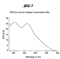
- the number of incident photons was determined by a photodetector, which measures a branched part of the beam, and compared with the current generated at the radiation wavelength. By dividing the number of electrons generated by the number of incident photons, the so-called Integrated Photon to Current Efficiency (IPCE) was determined as a function of the wavelength. An IPCE up to 0.7% at 440 nm was measured.
- IPCE Integrated Photon to Current Efficiency
- a cell was prepared as described in Example 6.
- RuL 3 4- was used as a sensitizer.
- the electrolyte consisted of a 50 g / l solution of the substance from Example 4 as a redox system in chloroform and about 25 g / l diethylimidiazolium trifluorosulfonate (lmTfl) as a conductive salt.
- the IPCE of the cell was approx. 3% at 440 nm. When irradiated with the full solar spectrum and 1000 W / m 2 , the short-circuit current was approx. 165 ⁇ Alcm 2 .
- a cell was prepared as described in Example 6.
- the electrolyte consisted of an approx. 25 g / l solution of the substance from Example 5 as a redox system in chloroform and approx. 25 g / l ethylmethylimidiazolium trifluorosulfonate (lmTfl) and approx. 10 g / l Li (CF 3 SO 2 ) 2 N) as conducting salts.
- the IPCE of the cell was approx. 35% at 440 nm.
- the short-circuit current was approx. 5.6 mA / cm 2 .
- the overall efficiency for energy conversion was approximately 2.5%.
- a cell was prepared as described in Example 6.
- the electrolyte consisted of an approximately 15 g / l solution of the substance from Example 5 as a redox system in glutaronitrile and approximately 25 g / l Ethylmethylimidiazolium trifluorosulfonate ((mTfl) as the conductive salt.
- the IPCE of the cell is approx. 38% at 440 nm.
- the short-circuit current was approx. 5.5 mA / cm 2.
- the overall efficiency for the energy conversion was about 2.5%.
Landscapes
- Chemical & Material Sciences (AREA)
- Engineering & Computer Science (AREA)
- Materials Engineering (AREA)
- Physics & Mathematics (AREA)
- Spectroscopy & Molecular Physics (AREA)
- Photovoltaic Devices (AREA)
- Hybrid Cells (AREA)
- Nitrogen Condensed Heterocyclic Rings (AREA)
Claims (13)
- Cellule photovoltaïque (10) caractérisée par un électrolyte (14), qui renferme un composé spiranique ou hétérospiranique conducteur de trous de formule (I)dissous,
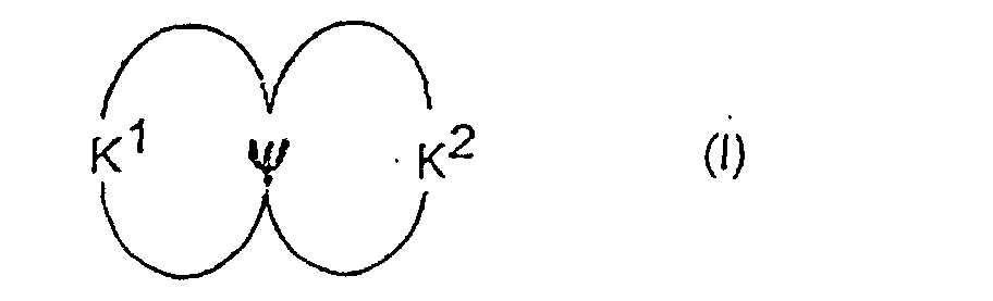
où- Ψ
- représente C, Si, Ge ou Sn et
- K1 et K2
- indépendamment l'un de l'autre représentent des systèmes conjugués, en tant que système redox.
- Cellule selon la revendication 1, caractérisée en ce que le composé spiranique ou hétérospiranique est un dérivé du spirofluorène de formule (II)où Ψ représente C, Si, Ge ou Sn et les groupes benzoïques peuvent être, indépendamment l'un de l'autre, substitués et/ou condensés.

- Cellule selon la revendication 2, caractérisée en ce que le dérivé du spirofluorène est un composé de formule (III)les symboles et les indices possèdent les significations suivantes :

- Ψ
- représente C, Si, Ge ou Sn,
- K1, L, M, N1, R1, R2, R3, R4
- sont identiques ou différents et représentent
a) un atome d'hydrogène, un groupe -NO2, -CN, -F ou - Cl,b) un reste alkyle linéaire ou ramifié présentant 1 à 20 atomes de carbone,b1) un ou plusieurs groupes CH2 non adjacents pouvant être remplacés par des groupes -O-, -S-, -CO-O-, -O-CO-, -O-CO-O-, NR5 ou - Si (CH3) 2- et/oub2) un ou plusieurs groupes CH2 pouvant être remplacés par des groupes -CH=CH-, -C≡C-, 1,4-phénylène, 1,4-cyclohexylène ou 1,3-cyclopentylène et/oub3) un ou plusieurs atomes d'hydrogène pouvant être remplacés par des atomes de F et/ou Cl, et/ouc) un des groupes suivants :


- X, Y1
- identiques ou différents représentent chacun un groupe =CR7- ou =N- ;
- Z
- représente un groupe -O-, -S-, -NR5-, -CRR-, - CR=CR- ou -CR=N- ;
- R5, R6
- identiques ou différents représentent chacun
- a) un atome d'hydrogène,
- b) un reste alkyle linéaire ou ramifié
présentant 1 à 20 atomes de carbone,
- b1) un ou plusieurs groupes CH2 non adjacents et non liés à l'atome d'azote pouvant être remplacés par des groupes -O-, -S-, -CO-O-, - O-CO-, -O-CO-O- ou -Si(CH3)2- et/ou
- b2) un ou plusieurs groupes CH2 pouvant être remplacés par des groupes - CH=CH-, -C≡C-, cyclopropane-1,2-diyle, 1,4-phénylène, 1,4-cyclohexylène ou 1,3-cyclopentylène, et/ou
- b3) un ou plusieurs atomes d'hydrogène pouvant être remplacés par des atomes de F et/ou Cl, et/ou
- b4) R5 et R6 conjointement peuvent aussi former un cycle ;
- c) représente un groupe phényle, biphényle, 1-naphtyle, 2-naphtyle, 2-thiényle, 2-furanyle ;
- R7, R8, R9, R10, R11, R12
- sont identiques ou différents
et représentent
- a) un atome d'hydrogène, un groupe -CN, -F, NO2 ou -Cl,
- b) un reste alkyle linéaire ou ramifié
présentant 1 à 20 atomes de carbone,
- b1) un ou plusieurs groupes CH2 non adjacents pouvant être remplacés par des groupes -O-, -S-, -CO-O-, -O-CO-, -O-CO-O-, -NR5 ou -Si(CH3)2- et/ou
- b2) un ou plusieurs groupes CH2 pouvant être remplacés par des groupes - CH=CH-, -C≡C-, cyclopropane-1,2-diyle, 1,4-phénylène, 1,4-cyclohexylène ou 1,3-cyclopentylène et/ou
- b3) un ou plusieurs atomes d'hydrogène pouvant être remplacés par des atomes de F et/ou Cl ;
- c) représente un groupe phényle, biphényle, 1-naphtyle, 2-naphtyle, 2-thiényle, 2-furanyle, O-phényle, -O-biphényle, -O-1-naphtyle, -O-2-naphtyle, -O-2-thiényle, -O-2-furanyle,
- m, n, p, q, r
- sont chaque fois identiques ou différents et valent 0, 1, 2, 3, 4, 5 ou 6.
- Cellule selon la revendication 3, caractérisée en ce que le dérivé du 9,9'-spirobifluorène est un composé de formule (IV)dans laquelle les symboles possèdent les significations suivantes :
 IVa) K1 = L = M = N1 =


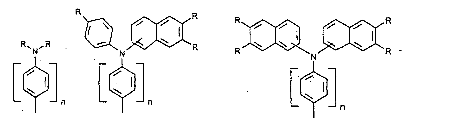
- R
- identiques ou différents représentent un atome d'hydrogène, un groupe alkyle, -O-alkyle, -S-alkyle, chacun présentant 1 à 20 atomes de carbone, phényle, biphényle, 1-naphtyle, 2-naphtyle, 2-thiényle, 2-furanyle, -O-phényle, -O-biphényle, -O-1-naphtyle, -O-2-naphtyle, -O-2-thiényle, -O-2-furanyle, dans ce contexte -O-alkyle/aryle, -S-alkyle/aryle, CN, NR2 ne peuvent pas être liés à l'atome d'azote ;
- n
- = 0, 1, 2, 3, 4 ;
H, COOR, CH2OR



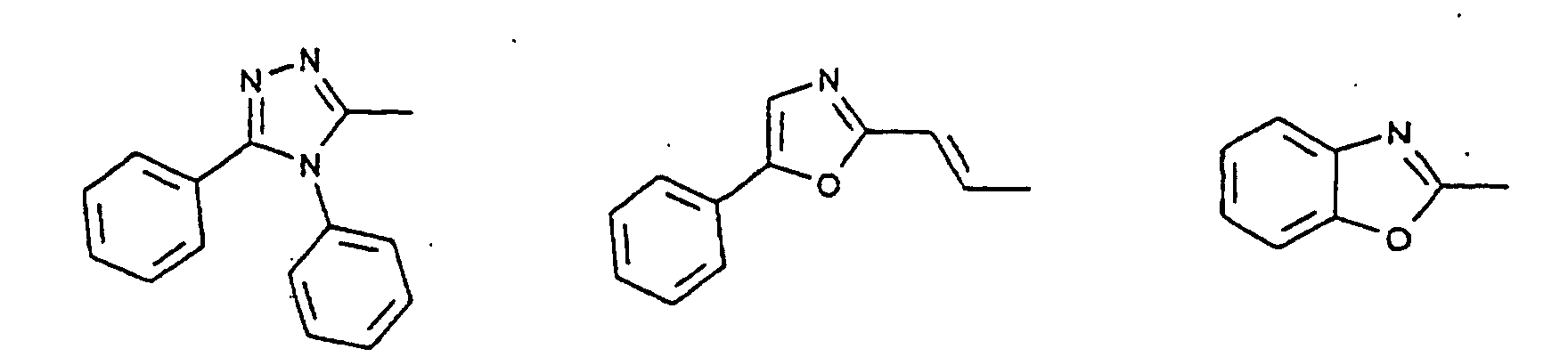


 les symboles et les indices possèdent les significations données ci-dessus ;
 IVb) K1 = N1 et est pris dans le groupe


 et L = M et est pris dans le groupe

H, COOR, CH2OR,


 et Q, P1 sont identiques ou différents pris dans le groupe
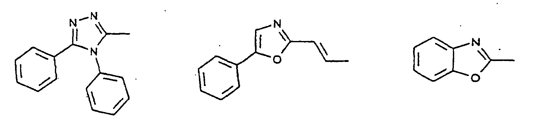


 H, COOR, CH2OR,


 les symboles et les indices possèdent les significations données ci-dessus ;
 IVc) K1 = M et est pris dans le groupe

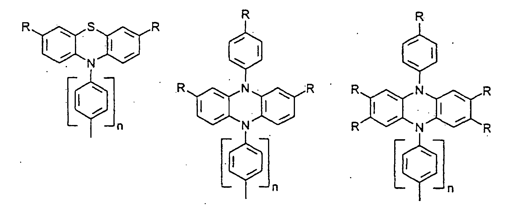
 et

M = N1 et est pris dans le groupe
H, COOR, CH2OR,


 et Q, P1 sont identiques ou différents pris dans le groupe


 H, COOR, CH2OR,
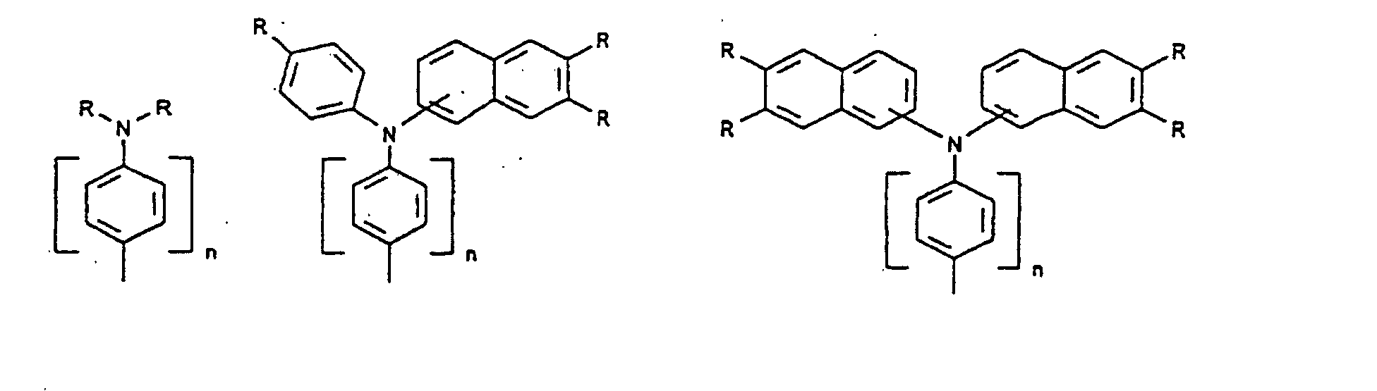



 les symboles et les indices possèdent les significations données ci-dessus.

- Cellule selon la revendication 4, caractérisée en ce que les symboles dans la formule (IV) possèdent les significations suivantes :IVaa) K1 = L = M = N1 et est pris dans le groupe :


 R13 représente un groupe -O-CH3, -O-C2H5, -S-CH3, -S-C2H5, de préférence -O-CH3, -S-CH3, de manière particulièrement préférée -O-CH3 ;

et Q = P1 et est pris dans le groupe
H, COOR14, CH2OR14, R14 représente un groupe alkyle linéaire ou ramifié présentant 1 à 12 atomes de carbone, de préférence 1 à 4 atomes de carbone ;
 IVba) K1 = L = M = N1 = Q = P1 et est pris dans le groupe


 R13 possède les significations données ci-dessus ;
 IVca) K1 = L = M = N1 et est pris dans le groupe


 et Q = H et P1 est pris dans le groupe H, COOR14, CH2OR14,

 R13, R14 possèdent les significations données ci-dessus.

- Cellule selon une ou plusieurs des revendications 1 à 5, caractérisée en ce que le potentiel de blocage de l'électrolyte liquide (14) est égal ou supérieur à 2,5 volts.
- Cellule selon la revendication 6, caractérisée en ce que l'électrolyte liquide (14) renferme un composé pris dans le groupe comprenant l'acétonitrile, le glutarodinitrile, le carbonate d'éthylène, le carbonate de propylène, le chlorobenzène et la 3-méthyl-2-oxazolidinone.
- Cellule selon une ou plusieurs des revendications précédentes 1 à 7, caractérisée en ce que l'électrolyte (14) renferme un sel conducteur.
- Cellule selon une ou plusieurs des revendications précédentes 1 à 8, caractérisée en ce qu'elle présente une couche photoabsorbante (12) qui renferme une matière semi-conductrice avec une bande interdite d'au moins 3 eV.
- Cellule photovoltaïque selon la revendication 9, caractérisée en ce que la matière semi-conductrice (12) est un oxyde métallique.
- Cellule photovoltaïque selon la revendication 9 ou 10, caractérisée en ce que la surface semi-conductrice (12) présente un facteur de rugosité >20.
- Cellule photovoltaïque selon une ou plusieurs des revendications précédentes 1 à 11, caractérisée en ce qu'elle renferme une couche photoabsorbante avec un colorant comme sensibilisant.
- Utilisation d'un composé conducteur de trous de formule (I)en tant que système redox dans un électrolyte liquide (14), où

- Ψ
- représente C, Si, Ge ou Sn et
- K1 et K2
- indépendamment l'un de l'autre représentent des systèmes conjugués.
Applications Claiming Priority (3)
| Application Number | Priority Date | Filing Date | Title |
|---|---|---|---|
| DE19711713 | 1997-03-20 | ||
| DE19711713A DE19711713A1 (de) | 1997-03-20 | 1997-03-20 | Photovoltaische Zelle |
| PCT/EP1998/001558 WO1998048433A1 (fr) | 1997-03-20 | 1998-03-18 | Cellule photovaltaique |
Publications (2)
| Publication Number | Publication Date |
|---|---|
| EP0968507A1 EP0968507A1 (fr) | 2000-01-05 |
| EP0968507B1 true EP0968507B1 (fr) | 2004-12-15 |
Family
ID=7824065
Family Applications (1)
| Application Number | Title | Priority Date | Filing Date |
|---|---|---|---|
| EP98913727A Expired - Lifetime EP0968507B1 (fr) | 1997-03-20 | 1998-03-18 | Cellule photovaltaique |
Country Status (5)
| Country | Link |
|---|---|
| US (1) | US6335480B1 (fr) |
| EP (1) | EP0968507B1 (fr) |
| JP (1) | JP2001525108A (fr) |
| DE (2) | DE19711713A1 (fr) |
| WO (1) | WO1998048433A1 (fr) |
Families Citing this family (68)
| Publication number | Priority date | Publication date | Assignee | Title |
|---|---|---|---|---|
| DE19711714A1 (de) * | 1997-03-20 | 1998-10-01 | Hoechst Ag | Spiroverbindungen und deren Verwendung |
| US6444189B1 (en) * | 1998-05-18 | 2002-09-03 | E. I. Du Pont De Nemours And Company | Process for making and using titanium oxide particles |
| US6949400B2 (en) * | 2002-01-25 | 2005-09-27 | Konarka Technologies, Inc. | Ultrasonic slitting of photovoltaic cells and modules |
| US7351907B2 (en) * | 2002-01-25 | 2008-04-01 | Konarka Technologies, Inc. | Displays with integrated photovoltaic cells |
| US6913713B2 (en) | 2002-01-25 | 2005-07-05 | Konarka Technologies, Inc. | Photovoltaic fibers |
| US20030192584A1 (en) * | 2002-01-25 | 2003-10-16 | Konarka Technologies, Inc. | Flexible photovoltaic cells and modules formed using foils |
| US20050284513A1 (en) * | 2002-08-08 | 2005-12-29 | Christoph Brabec | Chip card comprising an integrated energy converter |
| US7414188B2 (en) * | 2002-01-25 | 2008-08-19 | Konarka Technologies, Inc. | Co-sensitizers for dye sensitized solar cells |
| US7205473B2 (en) * | 2002-01-25 | 2007-04-17 | Konarka Technologies, Inc. | Photovoltaic powered multimedia greeting cards and smart cards |
| US20030192585A1 (en) * | 2002-01-25 | 2003-10-16 | Konarka Technologies, Inc. | Photovoltaic cells incorporating rigid substrates |
| US7186911B2 (en) * | 2002-01-25 | 2007-03-06 | Konarka Technologies, Inc. | Methods of scoring for fabricating interconnected photovoltaic cells |
| US6900382B2 (en) | 2002-01-25 | 2005-05-31 | Konarka Technologies, Inc. | Gel electrolytes for dye sensitized solar cells |
| US6706963B2 (en) | 2002-01-25 | 2004-03-16 | Konarka Technologies, Inc. | Photovoltaic cell interconnection |
| EP1160888A1 (fr) * | 2000-05-29 | 2001-12-05 | Sony International (Europe) GmbH | Matériau transportant de trous de charge et son utilisation dans des dipoitifs photoelectriques |
| US6919119B2 (en) * | 2000-05-30 | 2005-07-19 | The Penn State Research Foundation | Electronic and opto-electronic devices fabricated from nanostructured high surface to volume ratio thin films |
| US7042029B2 (en) | 2000-07-28 | 2006-05-09 | Ecole Polytechnique Federale De Lausanne (Epfl) | Solid state heterojunction and solid state sensitized photovoltaic cell |
| EP1176646A1 (fr) * | 2000-07-28 | 2002-01-30 | Ecole Polytechnique Féderale de Lausanne (EPFL) | Hétérojonction à l'état solide et cellule photovoltaique sensibilisé à l'état solide |
| DE10037391A1 (de) | 2000-08-01 | 2002-02-14 | Covion Organic Semiconductors | Strukturierbare Materialien, Verfahren zu deren Herstellung und deren Verwendung |
| JP3998903B2 (ja) * | 2000-09-05 | 2007-10-31 | 出光興産株式会社 | 新規アリールアミン化合物及び有機エレクトロルミネッセンス素子 |
| EP1289030A1 (fr) | 2001-09-04 | 2003-03-05 | Sony International (Europe) GmbH | Dopage d'un matériau transportant des trous de charge |
| CA2474491A1 (fr) * | 2002-01-25 | 2003-08-07 | Bill Beckenbaugh | Structures et substances pour colorer des piles solaires |
| CN1643629A (zh) * | 2002-01-25 | 2005-07-20 | 科纳卡科技有限公司 | 光电池结构和材料 |
| US20040057142A1 (en) * | 2002-07-10 | 2004-03-25 | Denglas Technologies, L.L.C. | Method of making stress-resistant anti-reflection multilayer coatings containing cerium oxide |
| WO2004025748A1 (fr) * | 2002-09-10 | 2004-03-25 | Agfa-Gevaert | Dispositif photovoltaique comprenant un compose 1,3,5-tris-aminophenyl-benzene |
| US20040211458A1 (en) * | 2003-04-28 | 2004-10-28 | General Electric Company | Tandem photovoltaic cell stacks |
| DE10340711A1 (de) | 2003-09-04 | 2005-04-07 | Covion Organic Semiconductors Gmbh | Elektronische Vorrichtung enthaltend organische Halbleiter |
| KR100569187B1 (ko) * | 2003-09-27 | 2006-04-10 | 한국과학기술연구원 | 시클로펜타디엔온으로부터 유도되는 화합물, 이의 제조방법 및 이를 이용한 el 소자 |
| DE102004021567A1 (de) | 2004-05-03 | 2005-12-08 | Covion Organic Semiconductors Gmbh | Elektronische Vorrichtungen enthaltend organische Halbleiter |
| DE102004021989A1 (de) * | 2004-05-04 | 2005-12-15 | Covion Organic Semiconductors Gmbh | Organische elektronische Vorrichtungen |
| DE102004030628A1 (de) * | 2004-06-24 | 2006-01-19 | Konarka Technologies, Inc., Lowell | Organisches elektronisches Element mit elektrisch leitfähiger semitransparenter Schicht |
| US20060070653A1 (en) * | 2004-10-04 | 2006-04-06 | Palo Alto Research Center Incorporated | Nanostructured composite photovoltaic cell |
| US7763794B2 (en) * | 2004-12-01 | 2010-07-27 | Palo Alto Research Center Incorporated | Heterojunction photovoltaic cell |
| US20060130890A1 (en) * | 2004-12-20 | 2006-06-22 | Palo Alto Research Center Incorporated. | Heterojunction photovoltaic cell |
| JP2009506360A (ja) * | 2005-08-22 | 2009-02-12 | コナルカ テクノロジーズ インコーポレイテッド | 組込型の光電池を備えるディスプレイ |
| CN103641726B (zh) | 2005-09-30 | 2015-10-28 | 株式会社半导体能源研究所 | 螺芴衍生物,发光元件用材料,发光元件,发光设备和电子设备 |
| US20070079867A1 (en) * | 2005-10-12 | 2007-04-12 | Kethinni Chittibabu | Photovoltaic fibers |
| GB2432718A (en) * | 2005-11-25 | 2007-05-30 | Seiko Epson Corp | Multicolour metal oxide electrochemical cell |
| US7820022B2 (en) * | 2005-11-28 | 2010-10-26 | General Electric Company | Photoelectrochemical cell and method of manufacture |
| DE102006006412A1 (de) * | 2006-02-13 | 2007-08-16 | Merck Patent Gmbh | Elektronisches Bauteil, Verfahren zu dessen Herstellung und dessen Verwendung |
| KR100810730B1 (ko) * | 2006-06-19 | 2008-03-07 | (주)인솔라텍 | 태양전지용 광흡수층의 제조방법 |
| US9112447B2 (en) * | 2006-11-03 | 2015-08-18 | Solera Laboratories, Inc. | Nano power cell and method of use |
| US8319092B1 (en) | 2006-11-03 | 2012-11-27 | Solera Laboratories, Inc. | Nano power cell and method of use |
| DE102008045664A1 (de) | 2008-09-03 | 2010-03-04 | Merck Patent Gmbh | Optoelektronische Vorrichtung |
| JP5254347B2 (ja) | 2007-10-24 | 2013-08-07 | メルク パテント ゲーエムベーハー | 光電子デバイス |
| DE102008045662A1 (de) | 2008-09-03 | 2010-03-04 | Merck Patent Gmbh | Optoelektronische Vorrichtung |
| DE102008045663A1 (de) | 2008-09-03 | 2010-03-04 | Merck Patent Gmbh | Fluorverbrückte Assoziate für optoelektronische Anwendungen |
| CN102265453B (zh) | 2008-10-29 | 2014-10-01 | 富士胶片株式会社 | 色素、使用其的光电转换元件、光电化学电池、及色素的制造方法 |
| JP5524557B2 (ja) | 2009-09-28 | 2014-06-18 | 富士フイルム株式会社 | 光電変換素子の製造方法、光電変換素子、および光電気化学電池 |
| JP5620081B2 (ja) | 2009-09-28 | 2014-11-05 | 富士フイルム株式会社 | 光電変換素子の製造方法 |
| RU2404486C1 (ru) * | 2009-11-24 | 2010-11-20 | Государственное образовательное учреждение высшего профессионального образования Московский государственный институт электронной техники (технический университет) (МИЭТ) | Твердотельный солнечный элемент на гибком носителе |
| US9012772B2 (en) * | 2010-10-22 | 2015-04-21 | Xerox Corporation | Photovoltaic device |
| EP2760847B1 (fr) | 2011-09-28 | 2018-04-25 | Sumitomo Chemical Co., Ltd. | Composés de spirobifluorène pour dispositifs émetteurs de lumière |
| JP5881578B2 (ja) | 2011-12-15 | 2016-03-09 | 富士フイルム株式会社 | 金属錯体色素、光電変換素子、色素増感太陽電池および色素溶液 |
| JP2013161751A (ja) | 2012-02-08 | 2013-08-19 | Fujifilm Corp | 光電変換素子およびその製造方法、これを用いた色素増感太陽電池 |
| JP5925541B2 (ja) | 2012-03-16 | 2016-05-25 | 富士フイルム株式会社 | 光電変換素子用金属錯体色素、光電変換素子、色素増感太陽電池、色素増感太陽電池用色素吸着組成液、色素増感太陽電池用半導体電極および色素増感太陽電池の製造方法 |
| JP6063359B2 (ja) | 2012-09-28 | 2017-01-18 | 富士フイルム株式会社 | 光電変換素子、色素増感太陽電池、金属錯体色素および金属錯体色素を溶解してなる色素溶液 |
| JP5913222B2 (ja) | 2012-09-28 | 2016-04-27 | 富士フイルム株式会社 | 光電変換素子および色素増感太陽電池 |
| JP2014082187A (ja) | 2012-09-28 | 2014-05-08 | Fujifilm Corp | 光電変換素子および色素増感太陽電池 |
| JP5913223B2 (ja) | 2012-09-28 | 2016-04-27 | 富士フイルム株式会社 | 金属錯体色素、光電変換素子、色素増感太陽電池、色素溶液および色素吸着電極 |
| JP5992389B2 (ja) | 2012-11-16 | 2016-09-14 | 富士フイルム株式会社 | 光電変換素子、色素増感太陽電池、金属錯体色素、色素溶液、色素吸着電極および色素増感太陽電池の製造方法 |
| JP5944372B2 (ja) | 2012-12-17 | 2016-07-05 | 富士フイルム株式会社 | 光電変換素子、色素増感太陽電池、金属錯体色素、色素溶液、色素吸着電極および色素増感太陽電池の製造方法 |
| WO2014111365A1 (fr) * | 2013-01-15 | 2014-07-24 | Basf Se | Oligomères et polymères de triangulène et leur utilisation en tant que matériau de conduction par trous |
| JP5972811B2 (ja) | 2013-02-22 | 2016-08-17 | 富士フイルム株式会社 | 光電変換素子、光電変換素子の製造方法および色素増感太陽電池 |
| JP6047513B2 (ja) | 2013-03-25 | 2016-12-21 | 富士フイルム株式会社 | 金属錯体色素、光電変換素子、色素増感太陽電池および金属錯体色素を含有する色素溶液 |
| EP3375017B1 (fr) | 2016-10-24 | 2021-08-11 | Indian Institute of Technology, Guwahati | Dispositif de collecte d'énergie électrique microfluidique |
| JP2020127007A (ja) * | 2019-02-01 | 2020-08-20 | 株式会社リコー | 光電変換素子、太陽電池モジュール、電源モジュール、及び電子機器 |
| CN111689867B (zh) * | 2020-06-05 | 2023-02-10 | 南京邮电大学 | 一种空穴传输层材料及其制备方法、钙钛矿太阳电池及其制备方法 |
| CN111848422B (zh) * | 2020-06-09 | 2021-07-06 | 山西美意呈科技有限公司 | 一种空穴传输材料及其在钙钛矿太阳能电池中的应用 |
Family Cites Families (3)
| Publication number | Priority date | Publication date | Assignee | Title |
|---|---|---|---|---|
| CH674596A5 (fr) | 1988-02-12 | 1990-06-15 | Sulzer Ag | |
| EP0676461B1 (fr) | 1994-04-07 | 2002-08-14 | Covion Organic Semiconductors GmbH | Composés spiro et leur application comme matières électroluminescentes |
| DE19533850A1 (de) | 1995-09-13 | 1997-03-27 | Hoechst Ag | Photovoltaische Zelle |
-
1997
- 1997-03-20 DE DE19711713A patent/DE19711713A1/de not_active Withdrawn
-
1998
- 1998-03-18 EP EP98913727A patent/EP0968507B1/fr not_active Expired - Lifetime
- 1998-03-18 JP JP54484398A patent/JP2001525108A/ja not_active Ceased
- 1998-03-18 WO PCT/EP1998/001558 patent/WO1998048433A1/fr not_active Ceased
- 1998-03-18 DE DE59812387T patent/DE59812387D1/de not_active Expired - Lifetime
- 1998-03-18 US US09/381,192 patent/US6335480B1/en not_active Expired - Lifetime
Also Published As
| Publication number | Publication date |
|---|---|
| JP2001525108A (ja) | 2001-12-04 |
| DE19711713A1 (de) | 1998-10-01 |
| EP0968507A1 (fr) | 2000-01-05 |
| DE59812387D1 (de) | 2005-01-20 |
| WO1998048433A1 (fr) | 1998-10-29 |
| US6335480B1 (en) | 2002-01-01 |
Similar Documents
| Publication | Publication Date | Title |
|---|---|---|
| EP0968507A1 (fr) | Cellule photovaltaique | |
| EP0850492B1 (fr) | Cellule photovoltaique avec un compose spirannique | |
| EP0968175B1 (fr) | Composes spiro et leur utilisation | |
| DE60029151T2 (de) | Photoelektrochemische Zelle mit einem Elektrolyten aus Flüssigkristallverbindungen | |
| DE69819712T2 (de) | Fotoempfindlicher metallkomplex und fotovoltaische zelle | |
| EP2655366B1 (fr) | Dérivés de monoimide de naphtalène et leur utilisation comme photosensibilisateurs dans des cellules solaires et photodétecteurs | |
| DE69930805T2 (de) | Photoelektrochemische Zelle | |
| EP2498315B1 (fr) | Cellule solaire organique | |
| WO2010094636A1 (fr) | Utilisation de dérivés triarylamines comme matériaux conducteurs de trous dans des cellules solaires organiques et cellules solaires organiques contenant ces dérivés triarylamines | |
| EP2903047A1 (fr) | Matériau de transport de trous et d'absorption de lumière pour cellules solaires à l'état solide | |
| EP3532480B1 (fr) | Complexes métalliques | |
| TWI472512B (zh) | 貴金屬釕類感光劑及其製備方法 | |
| EP0970086B1 (fr) | Composes spiro et leur utilisation | |
| EP2671271A1 (fr) | Elément photovoltaïque | |
| EP2092041A1 (fr) | Nouveau matériau de transport porteur de charge organique et hautement conducteur | |
| DE112006001200T5 (de) | Neue, eine Aminogruppe enthaltende heterozyklische Derivate und Sensibilisierungsfarbstoffe zur photoelektrischen Umwandlung, die die heterozyklischen Derivate enthalten | |
| EP3407361A1 (fr) | Matières fondues redox formées par des complexes de cuivre (i)/(ii) en tant que matériaux de transfert de charge et de stockage de charge | |
| EP0947006B1 (fr) | Detecteur de rayonnement | |
| EP4317134A1 (fr) | Composé ayant un groupe sulfonate, et élément de conversion photoélectrique utilisant ledit composé | |
| WO2024067923A1 (fr) | Composé chimique, composant optoélectronique comprenant au moins un tel composé chimique, et utilisation d'au moins un tel composé chimique dans un composant optoélectronique | |
| EP4548730A1 (fr) | Composant optoélectronique avec une couche photoactive réalisée sous la forme d'une hétérojonction plane | |
| DE102019118872A1 (de) | Organische Verbindung, und optoelektronisches Bauelement mit einer solchen organischen Verbindung |
Legal Events
| Date | Code | Title | Description |
|---|---|---|---|
| PUAI | Public reference made under article 153(3) epc to a published international application that has entered the european phase |
Free format text: ORIGINAL CODE: 0009012 |
|
| 17P | Request for examination filed |
Effective date: 19991020 |
|
| AK | Designated contracting states |
Kind code of ref document: A1 Designated state(s): DE FR GB NL |
|
| RAP1 | Party data changed (applicant data changed or rights of an application transferred) |
Owner name: AXIVA GMBH |
|
| RAP1 | Party data changed (applicant data changed or rights of an application transferred) |
Owner name: CELANESE VENTURES GMBH |
|
| 17Q | First examination report despatched |
Effective date: 20011106 |
|
| RAP1 | Party data changed (applicant data changed or rights of an application transferred) |
Owner name: COVION ORGANIC SEMICONDUCTORS GMBH |
|
| GRAP | Despatch of communication of intention to grant a patent |
Free format text: ORIGINAL CODE: EPIDOSNIGR1 |
|
| GRAS | Grant fee paid |
Free format text: ORIGINAL CODE: EPIDOSNIGR3 |
|
| GRAA | (expected) grant |
Free format text: ORIGINAL CODE: 0009210 |
|
| AK | Designated contracting states |
Kind code of ref document: B1 Designated state(s): DE FR GB NL |
|
| REG | Reference to a national code |
Ref country code: GB Ref legal event code: FG4D Free format text: NOT ENGLISH |
|
| REF | Corresponds to: |
Ref document number: 59812387 Country of ref document: DE Date of ref document: 20050120 Kind code of ref document: P |
|
| PGFP | Annual fee paid to national office [announced via postgrant information from national office to epo] |
Ref country code: GB Payment date: 20050307 Year of fee payment: 8 |
|
| PGFP | Annual fee paid to national office [announced via postgrant information from national office to epo] |
Ref country code: FR Payment date: 20050311 Year of fee payment: 8 |
|
| PGFP | Annual fee paid to national office [announced via postgrant information from national office to epo] |
Ref country code: NL Payment date: 20050322 Year of fee payment: 8 |
|
| GBT | Gb: translation of ep patent filed (gb section 77(6)(a)/1977) |
Effective date: 20050519 |
|
| PLBE | No opposition filed within time limit |
Free format text: ORIGINAL CODE: 0009261 |
|
| STAA | Information on the status of an ep patent application or granted ep patent |
Free format text: STATUS: NO OPPOSITION FILED WITHIN TIME LIMIT |
|
| 26N | No opposition filed |
Effective date: 20050916 |
|
| ET | Fr: translation filed | ||
| PG25 | Lapsed in a contracting state [announced via postgrant information from national office to epo] |
Ref country code: GB Free format text: LAPSE BECAUSE OF NON-PAYMENT OF DUE FEES Effective date: 20060318 |
|
| PG25 | Lapsed in a contracting state [announced via postgrant information from national office to epo] |
Ref country code: NL Free format text: LAPSE BECAUSE OF NON-PAYMENT OF DUE FEES Effective date: 20061001 |
|
| GBPC | Gb: european patent ceased through non-payment of renewal fee |
Effective date: 20060318 |
|
| NLV4 | Nl: lapsed or anulled due to non-payment of the annual fee |
Effective date: 20061001 |
|
| REG | Reference to a national code |
Ref country code: FR Ref legal event code: ST Effective date: 20061130 |
|
| PG25 | Lapsed in a contracting state [announced via postgrant information from national office to epo] |
Ref country code: FR Free format text: LAPSE BECAUSE OF NON-PAYMENT OF DUE FEES Effective date: 20060331 |
|
| PGFP | Annual fee paid to national office [announced via postgrant information from national office to epo] |
Ref country code: DE Payment date: 20150310 Year of fee payment: 18 |
|
| REG | Reference to a national code |
Ref country code: DE Ref legal event code: R119 Ref document number: 59812387 Country of ref document: DE |
|
| PG25 | Lapsed in a contracting state [announced via postgrant information from national office to epo] |
Ref country code: DE Free format text: LAPSE BECAUSE OF NON-PAYMENT OF DUE FEES Effective date: 20161001 |