EP0971417A2 - Photovoltaisches Bauelement und sein Herstellungsverfahren - Google Patents
Photovoltaisches Bauelement und sein Herstellungsverfahren Download PDFInfo
- Publication number
- EP0971417A2 EP0971417A2 EP99111326A EP99111326A EP0971417A2 EP 0971417 A2 EP0971417 A2 EP 0971417A2 EP 99111326 A EP99111326 A EP 99111326A EP 99111326 A EP99111326 A EP 99111326A EP 0971417 A2 EP0971417 A2 EP 0971417A2
- Authority
- EP
- European Patent Office
- Prior art keywords
- layer
- photovoltaic
- semiconductor
- bypass diode
- semiconductor junction
- Prior art date
- Legal status (The legal status is an assumption and is not a legal conclusion. Google has not performed a legal analysis and makes no representation as to the accuracy of the status listed.)
- Withdrawn
Links
- 238000004519 manufacturing process Methods 0.000 title description 8
- 239000004065 semiconductor Substances 0.000 claims abstract description 151
- 239000000758 substrate Substances 0.000 claims description 67
- 238000000034 method Methods 0.000 claims description 46
- 239000000463 material Substances 0.000 claims description 27
- 230000015572 biosynthetic process Effects 0.000 claims description 16
- 238000006243 chemical reaction Methods 0.000 abstract description 16
- 230000002035 prolonged effect Effects 0.000 abstract description 2
- 239000010408 film Substances 0.000 description 30
- 239000002184 metal Substances 0.000 description 15
- 229910052751 metal Inorganic materials 0.000 description 15
- 229910021417 amorphous silicon Inorganic materials 0.000 description 11
- 229920005989 resin Polymers 0.000 description 11
- 239000011347 resin Substances 0.000 description 11
- 238000005259 measurement Methods 0.000 description 9
- 238000005268 plasma chemical vapour deposition Methods 0.000 description 8
- 238000003475 lamination Methods 0.000 description 7
- RYGMFSIKBFXOCR-UHFFFAOYSA-N Copper Chemical compound [Cu] RYGMFSIKBFXOCR-UHFFFAOYSA-N 0.000 description 6
- 238000000151 deposition Methods 0.000 description 6
- 238000010438 heat treatment Methods 0.000 description 6
- XOLBLPGZBRYERU-UHFFFAOYSA-N tin dioxide Chemical compound O=[Sn]=O XOLBLPGZBRYERU-UHFFFAOYSA-N 0.000 description 6
- 239000000853 adhesive Substances 0.000 description 5
- 230000001070 adhesive effect Effects 0.000 description 5
- 229910052802 copper Inorganic materials 0.000 description 5
- 239000010949 copper Substances 0.000 description 5
- 239000011889 copper foil Substances 0.000 description 5
- 238000001704 evaporation Methods 0.000 description 5
- 238000012360 testing method Methods 0.000 description 5
- 229910045601 alloy Inorganic materials 0.000 description 4
- 239000000956 alloy Substances 0.000 description 4
- 229910052782 aluminium Inorganic materials 0.000 description 4
- 230000006378 damage Effects 0.000 description 4
- 230000003247 decreasing effect Effects 0.000 description 4
- 230000008021 deposition Effects 0.000 description 4
- 230000008020 evaporation Effects 0.000 description 4
- 229910052697 platinum Inorganic materials 0.000 description 4
- 229910052709 silver Inorganic materials 0.000 description 4
- 239000010409 thin film Substances 0.000 description 4
- 239000004642 Polyimide Substances 0.000 description 3
- 229910000577 Silicon-germanium Inorganic materials 0.000 description 3
- 229910052804 chromium Inorganic materials 0.000 description 3
- 238000005538 encapsulation Methods 0.000 description 3
- 238000005530 etching Methods 0.000 description 3
- 239000011521 glass Substances 0.000 description 3
- 239000007769 metal material Substances 0.000 description 3
- 229910052750 molybdenum Inorganic materials 0.000 description 3
- 229910052759 nickel Inorganic materials 0.000 description 3
- -1 polyethylene Polymers 0.000 description 3
- 229920001721 polyimide Polymers 0.000 description 3
- 238000007639 printing Methods 0.000 description 3
- 238000007650 screen-printing Methods 0.000 description 3
- 238000004544 sputter deposition Methods 0.000 description 3
- 239000010935 stainless steel Substances 0.000 description 3
- 229910001220 stainless steel Inorganic materials 0.000 description 3
- 239000000126 substance Substances 0.000 description 3
- 229910052719 titanium Inorganic materials 0.000 description 3
- XLOMVQKBTHCTTD-UHFFFAOYSA-N Zinc monoxide Chemical compound [Zn]=O XLOMVQKBTHCTTD-UHFFFAOYSA-N 0.000 description 2
- 230000003667 anti-reflective effect Effects 0.000 description 2
- 239000011230 binding agent Substances 0.000 description 2
- 229910052796 boron Inorganic materials 0.000 description 2
- 230000000052 comparative effect Effects 0.000 description 2
- 239000002131 composite material Substances 0.000 description 2
- 150000001875 compounds Chemical class 0.000 description 2
- 238000001035 drying Methods 0.000 description 2
- 238000005516 engineering process Methods 0.000 description 2
- 230000007613 environmental effect Effects 0.000 description 2
- 239000007789 gas Substances 0.000 description 2
- PJXISJQVUVHSOJ-UHFFFAOYSA-N indium(III) oxide Inorganic materials [O-2].[O-2].[O-2].[In+3].[In+3] PJXISJQVUVHSOJ-UHFFFAOYSA-N 0.000 description 2
- 239000011810 insulating material Substances 0.000 description 2
- 229910021424 microcrystalline silicon Inorganic materials 0.000 description 2
- 230000000737 periodic effect Effects 0.000 description 2
- 238000007747 plating Methods 0.000 description 2
- 229920000728 polyester Polymers 0.000 description 2
- 238000010248 power generation Methods 0.000 description 2
- 239000002994 raw material Substances 0.000 description 2
- 239000002904 solvent Substances 0.000 description 2
- 238000001228 spectrum Methods 0.000 description 2
- 238000010998 test method Methods 0.000 description 2
- 229910052718 tin Inorganic materials 0.000 description 2
- 229910052721 tungsten Inorganic materials 0.000 description 2
- ZOXJGFHDIHLPTG-UHFFFAOYSA-N Boron Chemical compound [B] ZOXJGFHDIHLPTG-UHFFFAOYSA-N 0.000 description 1
- 229910001369 Brass Inorganic materials 0.000 description 1
- OKTJSMMVPCPJKN-UHFFFAOYSA-N Carbon Chemical compound [C] OKTJSMMVPCPJKN-UHFFFAOYSA-N 0.000 description 1
- 229920000049 Carbon (fiber) Polymers 0.000 description 1
- 239000004952 Polyamide Substances 0.000 description 1
- 239000004698 Polyethylene Substances 0.000 description 1
- 239000004793 Polystyrene Substances 0.000 description 1
- 229920001328 Polyvinylidene chloride Polymers 0.000 description 1
- BQCADISMDOOEFD-UHFFFAOYSA-N Silver Chemical compound [Ag] BQCADISMDOOEFD-UHFFFAOYSA-N 0.000 description 1
- 229910001128 Sn alloy Inorganic materials 0.000 description 1
- 229910000831 Steel Inorganic materials 0.000 description 1
- 239000002390 adhesive tape Substances 0.000 description 1
- 229910052787 antimony Inorganic materials 0.000 description 1
- 229910052785 arsenic Inorganic materials 0.000 description 1
- QVGXLLKOCUKJST-UHFFFAOYSA-N atomic oxygen Chemical compound [O] QVGXLLKOCUKJST-UHFFFAOYSA-N 0.000 description 1
- 239000010951 brass Substances 0.000 description 1
- 230000005587 bubbling Effects 0.000 description 1
- CXKCTMHTOKXKQT-UHFFFAOYSA-N cadmium oxide Inorganic materials [Cd]=O CXKCTMHTOKXKQT-UHFFFAOYSA-N 0.000 description 1
- 229910052799 carbon Inorganic materials 0.000 description 1
- 239000006229 carbon black Substances 0.000 description 1
- 239000004917 carbon fiber Substances 0.000 description 1
- 230000015556 catabolic process Effects 0.000 description 1
- 229920002301 cellulose acetate Polymers 0.000 description 1
- 229910010293 ceramic material Inorganic materials 0.000 description 1
- 239000004020 conductor Substances 0.000 description 1
- 239000013078 crystal Substances 0.000 description 1
- 239000002178 crystalline material Substances 0.000 description 1
- 238000000354 decomposition reaction Methods 0.000 description 1
- 238000006731 degradation reaction Methods 0.000 description 1
- 238000010586 diagram Methods 0.000 description 1
- 230000000694 effects Effects 0.000 description 1
- 238000001810 electrochemical catalytic reforming Methods 0.000 description 1
- 239000003822 epoxy resin Substances 0.000 description 1
- 238000011156 evaluation Methods 0.000 description 1
- 239000000835 fiber Substances 0.000 description 1
- 239000011888 foil Substances 0.000 description 1
- 229910052733 gallium Inorganic materials 0.000 description 1
- 239000003365 glass fiber Substances 0.000 description 1
- 229920006015 heat resistant resin Polymers 0.000 description 1
- 238000007731 hot pressing Methods 0.000 description 1
- 239000012535 impurity Substances 0.000 description 1
- 229910052738 indium Inorganic materials 0.000 description 1
- 229910052742 iron Inorganic materials 0.000 description 1
- 238000010030 laminating Methods 0.000 description 1
- 229910052745 lead Inorganic materials 0.000 description 1
- 239000007791 liquid phase Substances 0.000 description 1
- 238000004518 low pressure chemical vapour deposition Methods 0.000 description 1
- 230000000873 masking effect Effects 0.000 description 1
- 229910044991 metal oxide Inorganic materials 0.000 description 1
- 150000004706 metal oxides Chemical class 0.000 description 1
- 239000013081 microcrystal Substances 0.000 description 1
- 229910052757 nitrogen Inorganic materials 0.000 description 1
- 229910052760 oxygen Inorganic materials 0.000 description 1
- 239000001301 oxygen Substances 0.000 description 1
- 230000036961 partial effect Effects 0.000 description 1
- 238000000059 patterning Methods 0.000 description 1
- 229910052698 phosphorus Inorganic materials 0.000 description 1
- 239000004033 plastic Substances 0.000 description 1
- 229920003023 plastic Polymers 0.000 description 1
- 229920002647 polyamide Polymers 0.000 description 1
- 229920000515 polycarbonate Polymers 0.000 description 1
- 239000004417 polycarbonate Substances 0.000 description 1
- 229910021420 polycrystalline silicon Inorganic materials 0.000 description 1
- 229920000647 polyepoxide Polymers 0.000 description 1
- 229920000573 polyethylene Polymers 0.000 description 1
- 229920005596 polymer binder Polymers 0.000 description 1
- 239000002491 polymer binding agent Substances 0.000 description 1
- 229920002223 polystyrene Polymers 0.000 description 1
- 239000004800 polyvinyl chloride Substances 0.000 description 1
- 229920000915 polyvinyl chloride Polymers 0.000 description 1
- 239000005033 polyvinylidene chloride Substances 0.000 description 1
- 238000002360 preparation method Methods 0.000 description 1
- 238000005546 reactive sputtering Methods 0.000 description 1
- 230000002829 reductive effect Effects 0.000 description 1
- 230000002441 reversible effect Effects 0.000 description 1
- 238000007789 sealing Methods 0.000 description 1
- 230000035945 sensitivity Effects 0.000 description 1
- 239000004332 silver Substances 0.000 description 1
- 238000009751 slip forming Methods 0.000 description 1
- 229910000679 solder Inorganic materials 0.000 description 1
- 230000003595 spectral effect Effects 0.000 description 1
- 239000010959 steel Substances 0.000 description 1
- 229910052715 tantalum Inorganic materials 0.000 description 1
- 238000002230 thermal chemical vapour deposition Methods 0.000 description 1
- 229920002803 thermoplastic polyurethane Polymers 0.000 description 1
- 238000002834 transmittance Methods 0.000 description 1
- 229910052720 vanadium Inorganic materials 0.000 description 1
- 238000004804 winding Methods 0.000 description 1
Images


Classifications
-
- H—ELECTRICITY
- H10—SEMICONDUCTOR DEVICES; ELECTRIC SOLID-STATE DEVICES NOT OTHERWISE PROVIDED FOR
- H10F—INORGANIC SEMICONDUCTOR DEVICES SENSITIVE TO INFRARED RADIATION, LIGHT, ELECTROMAGNETIC RADIATION OF SHORTER WAVELENGTH OR CORPUSCULAR RADIATION
- H10F71/00—Manufacture or treatment of devices covered by this subclass
- H10F71/10—Manufacture or treatment of devices covered by this subclass the devices comprising amorphous semiconductor material
- H10F71/107—Continuous treatment of the devices, e.g. roll-to roll processes or multi-chamber deposition
-
- H—ELECTRICITY
- H10—SEMICONDUCTOR DEVICES; ELECTRIC SOLID-STATE DEVICES NOT OTHERWISE PROVIDED FOR
- H10F—INORGANIC SEMICONDUCTOR DEVICES SENSITIVE TO INFRARED RADIATION, LIGHT, ELECTROMAGNETIC RADIATION OF SHORTER WAVELENGTH OR CORPUSCULAR RADIATION
- H10F19/00—Integrated devices, or assemblies of multiple devices, comprising at least one photovoltaic cell covered by group H10F10/00, e.g. photovoltaic modules
- H10F19/30—Integrated devices, or assemblies of multiple devices, comprising at least one photovoltaic cell covered by group H10F10/00, e.g. photovoltaic modules comprising thin-film photovoltaic cells
- H10F19/31—Integrated devices, or assemblies of multiple devices, comprising at least one photovoltaic cell covered by group H10F10/00, e.g. photovoltaic modules comprising thin-film photovoltaic cells having multiple laterally adjacent thin-film photovoltaic cells deposited on the same substrate
-
- H—ELECTRICITY
- H10—SEMICONDUCTOR DEVICES; ELECTRIC SOLID-STATE DEVICES NOT OTHERWISE PROVIDED FOR
- H10F—INORGANIC SEMICONDUCTOR DEVICES SENSITIVE TO INFRARED RADIATION, LIGHT, ELECTROMAGNETIC RADIATION OF SHORTER WAVELENGTH OR CORPUSCULAR RADIATION
- H10F19/00—Integrated devices, or assemblies of multiple devices, comprising at least one photovoltaic cell covered by group H10F10/00, e.g. photovoltaic modules
- H10F19/50—Integrated devices comprising at least one photovoltaic cell and other types of semiconductor or solid-state components
-
- H—ELECTRICITY
- H10—SEMICONDUCTOR DEVICES; ELECTRIC SOLID-STATE DEVICES NOT OTHERWISE PROVIDED FOR
- H10F—INORGANIC SEMICONDUCTOR DEVICES SENSITIVE TO INFRARED RADIATION, LIGHT, ELECTROMAGNETIC RADIATION OF SHORTER WAVELENGTH OR CORPUSCULAR RADIATION
- H10F77/00—Constructional details of devices covered by this subclass
- H10F77/10—Semiconductor bodies
- H10F77/16—Material structures, e.g. crystalline structures, film structures or crystal plane orientations
- H10F77/169—Thin semiconductor films on metallic or insulating substrates
- H10F77/1692—Thin semiconductor films on metallic or insulating substrates the films including only Group IV materials
-
- Y—GENERAL TAGGING OF NEW TECHNOLOGICAL DEVELOPMENTS; GENERAL TAGGING OF CROSS-SECTIONAL TECHNOLOGIES SPANNING OVER SEVERAL SECTIONS OF THE IPC; TECHNICAL SUBJECTS COVERED BY FORMER USPC CROSS-REFERENCE ART COLLECTIONS [XRACs] AND DIGESTS
- Y02—TECHNOLOGIES OR APPLICATIONS FOR MITIGATION OR ADAPTATION AGAINST CLIMATE CHANGE
- Y02E—REDUCTION OF GREENHOUSE GAS [GHG] EMISSIONS, RELATED TO ENERGY GENERATION, TRANSMISSION OR DISTRIBUTION
- Y02E10/00—Energy generation through renewable energy sources
- Y02E10/50—Photovoltaic [PV] energy
-
- Y—GENERAL TAGGING OF NEW TECHNOLOGICAL DEVELOPMENTS; GENERAL TAGGING OF CROSS-SECTIONAL TECHNOLOGIES SPANNING OVER SEVERAL SECTIONS OF THE IPC; TECHNICAL SUBJECTS COVERED BY FORMER USPC CROSS-REFERENCE ART COLLECTIONS [XRACs] AND DIGESTS
- Y02—TECHNOLOGIES OR APPLICATIONS FOR MITIGATION OR ADAPTATION AGAINST CLIMATE CHANGE
- Y02P—CLIMATE CHANGE MITIGATION TECHNOLOGIES IN THE PRODUCTION OR PROCESSING OF GOODS
- Y02P70/00—Climate change mitigation technologies in the production process for final industrial or consumer products
- Y02P70/50—Manufacturing or production processes characterised by the final manufactured product
-
- Y—GENERAL TAGGING OF NEW TECHNOLOGICAL DEVELOPMENTS; GENERAL TAGGING OF CROSS-SECTIONAL TECHNOLOGIES SPANNING OVER SEVERAL SECTIONS OF THE IPC; TECHNICAL SUBJECTS COVERED BY FORMER USPC CROSS-REFERENCE ART COLLECTIONS [XRACs] AND DIGESTS
- Y10—TECHNICAL SUBJECTS COVERED BY FORMER USPC
- Y10S—TECHNICAL SUBJECTS COVERED BY FORMER USPC CROSS-REFERENCE ART COLLECTIONS [XRACs] AND DIGESTS
- Y10S136/00—Batteries: thermoelectric and photoelectric
- Y10S136/291—Applications
- Y10S136/293—Circuits
Definitions
- the present invention relates to a photovoltaic element with excellent characteristics and high reliability and a method for producing the photovoltaic element, and more specifically to a photovoltaic element with excellent characteristics and a reduced loss in the energy conversion efficiency by forming a bypass diode under a current collecting electrode and a method for producing the photovoltaic element.
- a thin film type solar cell employing amorphous semiconductor is considered promising because of advantages such as of capable of forming a large-area solar cell, making the film thickness of a semiconductor thinner and depositing a film on an arbitrary substrate, in comparison with a single-crystal or polycrystal type solar cell.
- An amorphous silicon type solar cell is formed, for example, by stacking p-, i- and n-type thin amorphous silicon layers on a substrate. Also, for improving the energy conversion efficiency, there is contemplated so-called double or triple cell structure in which two or more of the above-mentioned pin junctions are superposed in series. At the light incident side and the back side of the above-mentioned semiconductor, there are formed a pair of electrodes, namely an upper electrode and a lower electrode, In the amorphous silicon type solar cell, because of the generally high sheet resistance of the semiconductor itself, there is required a transparent upper electrode covering the entire area of the semiconductor, which is usually composed of a transparent conductive film such as of SnO 2 or ITO.
- Such transparent conductive film functions also as an antireflective film.
- a current collecting grid electrode which is formed into a comb-shaped pattern so as not to hinder the entry of light, in other words, the irradiation of light, and a busbar is provided in order to collect the current from the grid electrode.
- a single solar cell photovoltaic element
- plural solar cells in parallel or serial connection.
- the largest difficulty in utilizing the plural cells (elements) in serial connection as described above lies in a fact, in a case of no electric power generation due to a part of the cells shadowed from the sunlight, for example, by a building or by accumulated snow, that a serially connected solar cell module can no longer generate an electric power even though other cells in the module still generate electric power, that the total voltage generated by the normally functioning cells is applied, as a backward voltage, to such shadowed cell. In case such backward voltage exceeds the tolerable voltage of the element, there may result destruction thereof.
- a diode parallel to the element but in a direction opposite to that of the semiconductor junction of the element.
- Such diode is generally called a bypass diode.
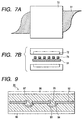
- Fig. 9 is a schematic view showing an example of the solar cell module utilizing such bypass diode.
- Fig. 9 shows a solar cell module 91 connected to bypass diodes, solar cells 92, bypass diodes 93, wirings 94, wirings 95 for serially connecting the solar cells 92, a glass plate 96, an encapsulating resin 97, and a back plastic material 98.
- the diode 93 has a thickness of about 3 mm in diameter in the case of an usual axial diode, the encapsulating resin 97 has to be made correspondingly thick.
- an object of the present invention is to provide a photovoltaic element formed by depositing a photovoltaic element portion and a bypass diode portion on the same substrate, while applying a semiconductor obtained by film formation to the portions, without involving a complex process, whereby the bypass diode portion does not reduce the effective area of the photovoltaic element with a high freedom in size, and a producing method therefor.
- the present invention provides a photovoltaic element comprising: a photovoltaic layer having a first semiconductor junction layer for generating a photoelectromotive force, a current collecting electrode provided at the light incident side of the photovoltaic layer, and a bypass diode connected in parallel, wherein the bypass diode is formed under the current collecting electrode as a bypass diode layer having a second semiconductor junction layer other than the first semiconductor junction layer of the photovoltaic layer.
- the present invention provides a method of producing a photovoltaic element, which comprises a step of forming, on a conductive substrate or a substrate with a conductive film formed thereon, a photovoltaic layer having a first semiconductor junction layer for generating a photoelectromotive force in plural positions with a predetermined space, a step of forming a bypass diode layer having a second semiconductor junction layer with a forward direction of a semiconductor junction opposite to that of the first semiconductor junction layer, on the substrate between the plural positions of the photovoltaic layer, and a step of forming a current collecting electrode so as to be connected to the photovoltaic layer and the bypass diode layer.
- the bypass diode layer is formed under the current collecting electrode, the photovoltaic layer, for example, having a pin or pn semiconductor junction deposited on a substrate, and the bypass diode layer can be easily formed by forming a film on the same substrate. Consequently the surface of the element can be planed and there can be dispensed with the step of wiring the bypass diode which is conducted by using a separate component in the conventional technology. Also the manufacturing process is simplified and is improved in reliability and production yield. Furthermore, the bypass diode layer does not sacrifice the effective area of the photovoltaic layer.
- the semiconductor material for forming the photovoltaic element may be crystalline or amorphous, but is preferably one capable of forming a thin semiconductor film on the substrate.
- Such thin semiconductor films are usually formed by an usual vacuum film forming process, but similar effects can also be obtained by a liquid phase process.
- the photovoltaic layer and the bypass diode layer may be simultaneously formed in the above-mentioned film forming process, but they may also be formed separately with different film forming apparatus.
- the film formation can be executed by a roll-to-roll process.
- there is a leaf-by-leaf process in other words, a sheet-by-sheet process in which the semiconductor layers are deposited in succession in the course of transportation of the substrate. This process is also preferable.
- the forward direction of each junction of the first and second semiconductor junction layers is mutually opposite. More specifically, the bypass diode layer as the second semiconductor junction layer is formed so as to have a pn or pin junction with a forward direction opposite to that of the photovoltaic layer as the first semiconductor junction layer, so as to be provided in parallel with respect to the photovoltaic layer, and so as to maintain the surface of the layers at the same level.
- a mask can be used.
- a plate for covering the substrate in a part of the vacuum chamber for example, in the width direction of the substrate where the current collecting electrode is to be formed, in order to prevent the film formation in such covered position.
- the photovoltaic element of the present embodiment is produced by forming a photovoltaic layer and the bypass diode layer on the same substrate, but the bypass diode layer has to be connected in parallel to the photovoltaic layer and formed so that the surface of the bypass diode is the same level as that of the photovoltaic layer. Also the forward directions of semiconductor junctions of the layers have to be mutually opposite to each other.
- Fig. 1 shows an equivalent circuit having the connection of the photovoltaic element and the bypass diode.
- Fig. 1 shows a diode component 11 of the photovoltaic layer, a DC power source component 12 of the photovoltaic layer, and a bypass diode layer 13.
- the above-described configuration can be obtained by forming one polar of the photovoltaic layer and one polar of the bypass diode layer on the same substrate, and mutually connecting the other polars with a metal electrode. Specifically, the photovoltaic layer and the bypass diode layer are both connected to the current collecting electrode as the metal electrode at the light incident side.
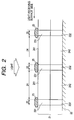
- Fig. 2 is a schematic cross-sectional view showing on example of the semiconductor layer configuration of the photovoltaic element according to the present embodiment.
- a semiconductor layer 21 is provided on a substrate 22, and linear current collecting electrodes 25 are further provided thereon with an interval therebetween.
- the side of the current collecting electrodes 25 is a light incident side.
- the semiconductor layer 21 has a bypass diode layer 23 and a photovoltaic layer 24.
- the bypass diode layer 23 and the photovoltaic layer 24 are alternately provided adjacent to each other.
- the current collecting electrode 25 is formed just on the bypass diode layer 23 so as not to hinder an incident light.
- the current collecting electrode 25 is connected to the bypass diode layer 23, and the ends of the current collecting electrode 25 are connected to the photovoltaic layer 24.
- the bypass diode layer 23 is composed of a plurality of semiconductor layers 231 and 232 different in characteristics from each other in this order from the light-receiving side toward the side of the substrate 22.
- Fig. 2 shows one example in which the bypass diode layer has a two-layered structure of a p-type and an n-type layers.
- the photovoltaic layer 24 is composed of a plurality of semiconductor layers 241 and 242 different in characteristics from each other, and as one example the photovoltaic layer is composed of a p-type and an n-type layers.
- the semiconductor layers 231 and 241 are different in characteristics from each other, in other words, when one semiconductor layer is a p-type layer, the other semiconductor layer is an n-type layer. Similarly, the semiconductor layers 232 and 242 are different in characteristics from each other.
- the photovoltaic layer and the bypass diode layer are laterally formed adjacent to each other on the same substrate, and are formed in mutually parallel belt-like shape of the substantially same length, both in the roll-troll feeding method or in the leaf-by-leaf feeding method.
- the photovoltaic element of the present embodiment may be produced, except for one shown in Fig. 2, by simultaneously forming at least one of the semiconductor layers constituting the first semiconductor junction layer and at least one of those constituting the second semiconductor junction layer with the same material.
- the intrinsic layer may be continuously extended over both semiconductor junction layers.
- the intrinsic layer i-type layer
- the intrinsic layer may be provided in common to both the first and second semiconductor junction layers, though the order of deposited layers of the pin junctions is different in the first and second semiconductor junction layers.
- Such configuration may be obtained by forming the i-type layers of both junction layers with the same material at the same time in formation of the first and second semiconductor junctions layers with a pin junction. After forming the i-type layer, the surface of a layer formed on the i-type layers on the both junction layers can be adjusted to the same level.
- the first semiconductor junction layer as the photovoltaic layer may have a triple cell structure of three stacked semiconductor layers each having a pin or pn junction
- the second semiconductor junction layer as the bypass diode layer may have a single cell structure of a single semiconductor layer having a pin or pn junction.
- the bypass diode layer can be formed in formation of the p-type layer of the bottom pin junction, the i-type layer of the middle pin junction and the n-type layer of the top pin junction.
- the third, fifth and seventh layers among nine layers constituting the first semiconductor junction layer are respectively formed simultaneously with the first, second and third layers constituting the second semiconductor junction layer by using the same materials.
- the third layer among nine layers constituting the first semiconductor junction layer is formed simultaneously with the first layer constituting the second semiconductor junction layer by using the same material;
- the fifth layer among nine layers constituting the first semiconductor junction layer is formed simultaneously with the second layer constituting the second semiconductor junction layer by using the same material;
- the seventh layer among nine layers constituting the first semiconductor junction layer is formed simultaneously with the third layer constituting the second semiconductor junction layer by using the same material.
- the semiconductor layers constituting the first semiconductor junction layer can be composed of thin semiconductors such as amorphous silicon, microcrystalline silicon or polycrystalline silicon.
- the semiconductor material constituting the i-type layer can include so-called Group IV or Group VI alloy type amorphous or microcrystalline semiconductor such as a-Si:H, a-Si:F, a-Si:H:F, a-SiGe:H, a-SiGe:F, a-SiGe:H:F, a-SiC:H, a-SiC:F or a-SiC:H:F.
- the semiconductor material constituting the p-type or n-type layer can be obtained by doping the above-mentioned semiconductor material constituting the i-type layer with a valence electron controlling substance.
- a valence electron controlling substance for obtaining the p-type semiconductor there is employed a compound containing an element of Group III of the periodic table.
- the element of Group III includes B, Al, Ga and In.
- the valence electron controlling substance for obtaining the n-type semiconductor there is employed a compound containing an element of Group V of the periodic table.
- the element of Group V includes P, N, As and Sb.
- the amorphous or microcrystalline silicon semiconductor layer can be formed by a known method such as evaporation, sputtering, plasma CVD, microwave plasma CVD, VHFCVD, ECR, thermal CVD or LPCVD.
- a known method such as evaporation, sputtering, plasma CVD, microwave plasma CVD, VHFCVD, ECR, thermal CVD or LPCVD.
- the RF plasma CVD in which a raw material gas is decomposed by RF plasma and deposited onto the substrate.
- the RF plasma CVD process is associated with drawbacks that the decomposition efficiency of the raw material gas is as low as about 10% and that the deposition rate is as low as 1 to 10 ⁇ /sec, and microwave plasma CVD and VHF plasma CVD are contemplated in order to overcome these drawbacks.
- the photovoltaic element of the present invention is applicable also to so-called tandem cell in which two or more semiconductor junctions are stacked in order to improve the spectral sensitivity or to increase the output voltage.
- a deposition preventing plate for preventing the film deposition in the vacuum chamber.
- the leaf-by-leaf feeding apparatus may be used.
- the first semiconductor junction layer of the photovoltaic layer is formed in the order of n, i and p, while the second semiconductor junction layer of the bypass layer is formed in the order of p, i and n.
- the substrate is not essential in the present invention, an advantageous configuration can be obtained by forming thin semiconductor films on a substrate with an appropriate shape or size.
- the substrate when the substrate is composed of a metal, the substrate can be used not only for mechanically supporting the thin films such as the semiconductor layers and the electrode layer, but also for functioning as an electrode (first electrode).
- the substrate can be composed of a conductive or insulating material, but when the substrate is composed of an insulating material, the surface of the substrate is subjected to a conductive treatment to utilize it as an electrode.
- Such substrate is required to have heat resistance capable of withstanding the heating temperature in formation of the semiconductor layers and the electrode layer. It is also required to be of a continuous long form in the case of the roll-to-roll film-forming process, and further required to be dimensionally stable without elongation, in order to enable winding under a tension.
- the preferred conductive substrate includes a thin plate composed of a metal such as Fe, Ni, Cr, Al, Mo, Au, Nb, Ta, V, Ti, Pt, Pb or Ti, an alloy thereof such as brass or stainless steel, or a composite material thereof, a carbon sheet or a zinc-plated steel plate.
- a metal such as Fe, Ni, Cr, Al, Mo, Au, Nb, Ta, V, Ti, Pt, Pb or Ti
- an alloy thereof such as brass or stainless steel
- a composite material thereof a carbon sheet or a zinc-plated steel plate.
- the stainless steel because of various features such as satisfactory heat resistance to the heating temperature at the film formation and a high mechanical strength suitable for continuous film formation such as a roll-to-roll system, for example, even in the case of a thickness as small as 0.15 mm.
- a preferred insulating substrate includes a heat-resistant resin film or sheet such as of polyester, polyethylene, polycarbonate, cellulose acetate, polypropoylene, polyvinyl chloride, polyvinylidene chloride, polystyrene, polyamide, polyimide, epoxy resin, a composite material of such resin material with glass fibers, carbon fibers or boron fibers, glass or a ceramic material. Particularly preferred is a glass or polyimide substrate.
- the photovoltaic layer may have an upper electrode at the light incident side thereof.
- Such upper electrode is not essential in the present invention, but is provided for reducing the sheet resistance in case the first semiconductor junction layer is composed of a material of a high resistance such as amorphous silicon. It is not necessary to provide the upper electrode when the sheet resistance is low as in the case of crystalline materials including microcrystal.
- the upper electrode serves to gather the electromotive force generated in the first semiconductor junction layer, and functions in pair with the first electrode at the substrate side.
- the upper electrode is required to gather the current in a direction parallel to the substrate in case of utilizing the semiconductor material of a high sheet resistance such as amorphous silicon, and preferably has a sheet resistance not exceeding 300 ⁇ / ⁇ .
- the thickness of the upper electrode must be designed so as to have a sufficiently low resistance and satisfactory transparency, and in some cases, to minimize the light reflection at the wavelength of the light to be transmitted, based on the light interference condition. For example, in order to minimize the reflection of the light of 550 nm by using ITO as the upper electrode, there is preferred a thickness of about 700 ⁇ . Also, the above-mentioned upper electrode (second electrode) is positioned at the light incident side and preferably has a light transmittance of at least 85% in order that the light from the sun or a white fluorescent lamp is efficiently absorbed by the semiconductor layer.
- the upper electrode (second electrode) can be formed with a known method such as evaporation, sputtering or reactive sputtering.
- the current collecting electrodes are provided at an interval therebetween on the light-receiving side. Further, the current collecting electrodes are formed in a comb-like shape on the upper (second) electrode, and is formed as an electrode of low resistance for improving the energy conversion efficiency of the photovoltaic element, because the current collection directly from the second electrode of high sheet resistance results in a low energy conversion efficiency by the high series resistance.
- the width and pitch of the current collecting electrodes are designed so as to minimize the electrical resistance in current collection and the shadow loss.
- the current collecting electrode is required to have a low specific resistivity, and not to constitute a series resistance with respect to the photovoltaic element.
- the specific resistivity is preferably within a range of 10 -2 to 10 -6 ⁇ cm.
- the current collecting electrode is composed of a metal such as Ti, Cr, Mo, W, Al, Ag, Ni, Cu, Sn, Pt or Cu, an alloy thereof or solder.
- the current collecting electrode can be formed by printing of so-called conductive paste, which is consisted of the above-mentioned powdered metallic material mixed with a polymer binder and a solvent for the binder in appropriate ratio, plating of the above-mentioned metallic material, or placing of a wire of the above-mentioned metallic material.
- the comb-shaped current collecting electrode may be formed in a desired shape and position by sputtering, resistance heating or CVD, while employing a mask of a desired shape. There may also be employed a method of evaporating a metal over the entire surface and patterning the obtained metal layer by etching, a method of directly forming the pattern of the current collecting electrode by photo CVD, a method of forming a mask of the negative pattern of the current collecting electrode followed by plating, or a method of screen printing of a conductive paste.
- the above-mentioned screen printing method consists of printing the conductive paste through a screen having a desired pattern on a polyester or stainless steel mesh, and can provide a current collecting electrode of a width of about 50 ⁇ m at minimum.
- the printing can be advantageously executed in a commercially available screen printing machine.
- the screen printed conductive paste is heated in a drying oven, in order to crosslink the binder and to evaporate the solvent.
- the drying oven can be a hot air oven or an in
- the current collecting electrode may also be formed with a metal wire.
- a metal wire such as of Ti, Cr, Mo, W, Al, Ag, Ni, Cu, Sn, Pt or Cu with a diameter preferably within a range of 50 ⁇ m to 200 ⁇ m.
- the current collecting electrode can be provided by adhering the metal wire to the second electrode with a conductive adhesive.
- the metal wire may be coated in advance with the conductive adhesive.
- the current collecting electrode may be provided directly on the bypass diode layer. In this case, the upper electrode must be connected to both of the photovoltaic layer and the current collecting electrode.
- the busbar may be employed if necessary.
- the busbar serves as an electrode for further collecting the currents in the current collecting electrode to an end.
- the busbar can be composed of a metal such as Ag, Pt or Cu or an alloy thereof.
- the busbar may be formed in a wire, a foil or a conductive paste similar to that employed for the current collecting electrode.
- the foil-shaped busbar may be composed, for example, of a copper foil or a tin-plated copper foil, optionally coated with an adhesive.
- the busbar may be formed by fixing a metal wire with conductive adhesive, or by adhering a copper foil. Otherwise it may be formed in a similar manner to the case of the current collecting electrode.
- the second semiconductor junction layer in the bypass diode layer is composed of thin semiconductor layers deposited on the aforementioned substrate and having at least a pn or pin junction as described above, and is formed by using almost the same materials and method as in the case of the first semiconductor junction layer.
- the second semiconductor junction layer may be formed simultaneously with or separately from the first semiconductor junction layer.
- the bypass diode performs a function of bypassing an operation current generated by other photovoltaic elements connected in series, and is required to be capable of bypassing the operation current at the operation point of the photovoltaic element.
- the operation current and the operation voltage of the bypass diode are determined according to the desired specifications of the photovoltaic elements.
- the operation current of the bypass diode may be increased or decreased, for example, by increasing or decreasing the area of the bypass diode layer or the impurity density in the semiconductor layer.
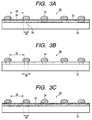
- FIGs. 3A to 3C are schematic cross-sectional views showing bypass diode portions in three kinds of the photovoltaic elements with bypass diodes, according to the examples of the present invention.
- each of photovoltaic elements 30 is composed of a photovoltaic layer 32 having a semiconductor junction layer for generating a photoelectromotive force, a current collecting electrode 34 provided on a bypass diode layer 38.
- the bypass diode layer 38 is composed of a second semiconductor junction layer other than the first semiconductor junction layer in the photovoltaic layer 32.
- each of the semiconductor junction layers of the photovoltaic layer 32 and the bypass diode layer 38 is formed so as to have one pin junction. There is also provided an upper electrode 33 at the light-receiving surface side. An intrinsic layer 36 of the bypass diode layer 38 and an intrinsic layer 35 of the photovoltaic layer 32 are formed separately.
- each of the semiconductor junction layers of the photovoltaic layer 32 and the bypass diode layer 38 is formed so as to have one pn junction formed by thin films and there is no upper electrode because the thin films have a small sheet resistance.
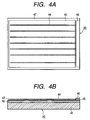
- Figs. 4A and 4B are respectively a plan view seen from the light-receiving surface side and a cross-sectional view of the entire photovoltaic element having the configurations shown in Figs. 3A to 3C.
- Fig. 4B is a cross-sectional view along the current collecting electrode 44.
- the photovoltaic element shown in Fig. 3A was produced in the following manner. At first, a sufficiently decreased and rinsed substrate 31 of SUS430BA (0.2 mm in thickness) was placed in a RF plasma CVD apparatus not shown in the drawings and then subjected to the deposition of n-type, i-type and p-type layers in this order, thereby obtaining the semiconductor junction layer of the photovoltaic layer 32. In this operation, the substrate 31 was masked with a polyimide adhesive tape in lines of a width of 1 mm spaced with a gap of 5 mm therebetween, in order to prevent formation of the semiconductor junction layer in thus masked area. That is, the semiconductor junction layer of the photovoltaic layer 32 was formed in plural positions mutually separated by a gap of 1 mm.
- the substrate 31 having the semiconductor junction layer formed thereon was placed in an evaporation apparatus of resistance heating type not shown in the drawings, and subjected to the evaporation of In-Sn alloy by resistance heating under an internal pressure of 1 ⁇ 10 -4 Torr while introducing oxygen to deposit a transparent ITO upper electrode 33 of a thickness of 700 ⁇ having also an antireflective effect, thereby completing the photovoltaic layer 32.
- the above-mentioned mask was removed from the substrate 31, the photovoltaic layer 32 was masked instead, and the above-mentioned CVD film forming apparatus was employed to deposit p-type, i-type and n-type layers in this order to complete the bypass diode 38.
- the bypass diode layer 38 having the p-type, i-type and n-type layers was formed so that the surface of the bypass diode layer had the same level as that of the photovoltaic layer 32 adjacent to the bypass diode layer.
- the upper electrode 33 was formed on the bypass diode layer 38 so that the surface of the upper electrode 33 formed on the bypass diode layer 33 had the same level as that of the upper electrode formed on the photovoltaic layer 32.
- busbar 46 consisting of a copper foil of a thickness of 100 ⁇ m was adhered onto the current collecting electrode 44 so as to overlap with the insulating tape 45, whereby the photovoltaic element with the bypass diode shown in Fig. 3A was completed.
- each encapsulated sample was subjected to the measurement of the initial characteristics according to the output measuring method for the amorphous solar cell module, defined in JIS C8935.
- the energy conversion efficiency was determined by measuring the solar cell characteristics with a solar simulator light source (manufactured by SPIRE Co., hereinafter referred to as "simulator") of a light amount of 100 mW/cm 2 at an AM1.5 global sunlight spectrum. The obtained characteristics were satisfactory with little fluctuation, and the shadow loss was 4.5%.
- the samples were subjected to the measurement of reliability, according to the temperature-humidity cycle test A-2 defined in the environmental and durability test methods for the amorphous solar cell module in JIS C8938. Specifically, the sample was placed in a constant temperature/humidity container with controllable temperature and humidity, and was subjected to a cycle test of varying the temperature from -40°C to +85°C (85% relative humidity) ten times. Under the observation after testing, the samples showed satisfactory appearance without any peeling or bubbling of the laminating materials.
- the photovoltaic element of the present example was produced by integrating the bypass diode portion with the photovoltaic layer and providing the bypass diode layer 38 under the current collecting electrode 34. It is therefore possible to reduce the shadow loss, to plane the entire photovoltaic element, thereby allowing to employ thinner lamination materials and to obtain satisfactory reliability.
- a photovoltaic elements 92 with the conventional bypass diode 93 as shown in Fig. 9 was produced in substantially the same manner as in Example 1. More specifically, by using the same method as in Example 1, there was conducted up to the formation of an upper electrode (not shown in the drawings) on a substrate (not shown in the drawings), and then the current collecting electrode and the busbar were formed thereon to obtain the photovoltaic element 92.
- the diode 93 was connected to the photovoltaic element 92, and lamination (encapsulation) was executed in the same manner as in Example 1 to obtain a solar cell module 91.
- the lamination material was varied in thickness as 250 ⁇ m, 500 ⁇ m, 1 mm and 3 mm.
- the filing was insufficient at thicknesses not larger than 1 mm, but satisfactory at a thickness of 3 mm.
- a photovoltaic element module (not shown in the drawings) formed by serial connection of the photovoltaic elements 40 with bypass diode having the configuration shown in Figs. 4A and 4B. Specifically, at first there were produced ten photovoltaic elements with bypass diodes of the configuration shown in Figs. 4A and 4B. The busbar 46 of each photovoltaic element was connected through an interconnector to the substrate 41 of an adjacent photovoltaic element, and this connection was repeatedly conducted to obtain ten photovoltaic elements connected in series.
- the photovoltaic elements connected in series were subjected to encapsulation in the following manner. Specifically, at first, EVA resins were stacked on and under each substrate 41, i.e., on the light incident side and the opposite side thereof. The EVA resin on the light incident side had a thickness of 250 ⁇ m. Then a fluororesin film was further stacked on the light incident side, while a metal plate was stacked on the back side. Then the stacked components were subjected to vacuum lamination in a vacuum lamination for 60 minutes at 150°C.
- the encapsulated photovoltaic elements connected were subjected to the measurement of the initial characteristics according to the output measuring method for the amorphous solar cell module, defined in JIS C8935.
- the energy conversion efficiency was determined by measuring the solar cell characteristics with the solar simulator light source (manufacture by SPIRE Co., hereinafter referred to as "simulator") of a light amount of 10 mW/cm 2 at an AM1.5 global sunlight spectrum. The obtained characteristics were satisfactory with little fluctuation.
- the reliability was measured by the hot spot test A-1 defined in the environmental and durability test methods for the amorphous solar cell module in JIS C8938. Specifically, at first the sample was irradiated with the light of 100 mW/cm 2 in the solar simulator, while one photovoltaic element among the serially connected ten photovoltaic elements-containing module (ten photovoltaic elements connected in series) was shadowed. After standing for ten minutes in this condition, the solar cell characteristics were measured with the simulator in the same manner as in the measurement of the initial characteristics, but no significant degradation was observed in comparison with the initial conversion efficiency.
- the solar cell comprising the photovoltaic elements of the present example has satisfactory characteristics, also can avoid the hot spot damage resulting from a partial shadow, and also has high reliability.
- Example 1 For the purpose of comparison, conventional photovoltaic elements without the bypass diode were produced in substantially the same manner as in Example 1. More specifically, at first there was executed the same method as in Example 1 up to the preparation of the upper electrode on the substrate. Then an insulating layer with an adhesive material was adhered to both ends of the substrate, and the current collecting electrode was formed in the same manner as in Example 1. Then the busbar consisting of a copper foil was stacked to complete the photovoltaic element.
- the encapsulated photovoltaic elements were subjected to the measurement of the initial characteristics in the same procedure as in Example 1, and to the evaluation of the reliability in the same manner as in Example 2.
- the measurement after the tests revealed that the energy conversion efficiency decreased by about 7.5%.
- the cause of the decrease in the efficiency was analyzed and attributed to the shunting of the photovoltaic element in the shadowed area which was generated by the application of a reverse bias to such shadowed photovoltaic element.
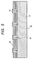
- Fig. 5 is a cross-sectional view of the photovoltaic element of Example 3 of the present invention.
- the photovoltaic layer 52 in this photovoltaic element 50 has a triple cell structure, in which the semiconductor junction layer consists of three stacked semiconductor layers each including a pin junction.
- the bypass diode layer 53 has a single cell structure, in which the semiconductor junction layer includes only one semiconductor layer having a pin junction.
- the photovoltaic layer 52 and the bypass diode layer 53 are formed laterally adjacent to each other on the same substrate 51, wherein the forward directions of the respective semiconductor junction layers have mutually opposite to each other.
- the photovoltaic layer 52 and the bypass diode layer 53 are connected to the current collecting diode 54 at the light incident side.
- there can be formed a photovoltaic element comprising a photovoltaic layer 52 having a triple cell structure of pn junctions and a bypass diode layer 53 having a single cell structure of a pn junction.
- Figs. 6A, 6B, 7A and 7B show a method of forming the photovoltaic element 50 in a roll-to-roll process by a triple cell film-forming apparatus 60.
- Fig. 6A is a schematic cross-sectional view of the film-forming apparatus utilizing the roll-to-roll process.
- film-forming chambers 62 to 70 there are arranged film-forming chambers 62 to 70 in this order.
- the chamber 62, 65 and 68 are used for forming n-type layers
- the chambers 63, 66 and 69 are used for forming i-type layers
- the chambers 64, 67 and 70 are used for forming p-type layers to obtain triple cells.
- each chamber 72 is provided with baffle plates 73 for intercepting the plasma as shown in Fig. 7B, thereby preventing film formation on a part of the substrate 51.
- the baffle plates 73 are positioned corresponding to the plural current collecting electrodes 54, and are provided with a width substantially equal to that of the current collecting electrode 54.
- the p-type layer of the bottom layer, the i-type layer of the middle layer and the n-type layer of the top layer is formed on a part of the substrate 51 to complete the bypass diode layer 53 on the substrate, while forming the semiconductor junction layers of the photovoltaic layer 52 on the substrate.
- the third, fifth and seventh layers among nine semiconductor layers constituting the semiconductor junction layer of the photovoltaic layer 52 are respectively formed simultaneously with the first, second and third layers of three semiconductor layers constituting the semiconductor junction layer of the bypass diode layer 53, by using the same materials.
- a coiled long SUS430 substrate 51 was set in a feeding chamber 61 of the film-forming apparatus and was transported at a constant speed to a wind-up chamber 71 at the other end, and the photovoltaic layer 52 and the bypass diode layer 53 were formed on the substrate 51 as shown in Fig. 6B in the course of transportation.
- another vacuum chamber not shown in the drawings was used to form the upper electrode only on the photovoltaic layer 52.
- the long substrate 51 was cut into sheets of a length of 20 cm. Subsequently, an upper electrode at the periphery of each cut substrate was removed by etching as in Example 1, and a current collecting electrode and a busbar were formed.
- the obtained samples were subjected to the measurement of the initial characteristics in the same manner as in Example 1.
- the samples showed satisfactory conversion efficiency within a range of 8.5 ⁇ 1.5%, with a shadow loss as small as 4.5% and with little fluctuation.
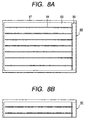
- Example 1 At first there was executed the process of Example 1 up to the formation of the upper electrode 83, and the upper electrode 83 in a portion to be divided and in the periphery of the substrate to form a region 87 in which the semiconductor was exposed. Then the current collecting electrode 84 was fixed in the same manner as in Example 1. Further, the current collecting electrode 84 and the busbar 89 were fixed with a silver paste to complete the photovoltaic element 80 with a bypass diode of a configuration shown in Fig. 8A.
- the photovoltaic element 80 thus produced was subjected to the measurement of the conversion efficiency.
- the photovoltaic element was divided into four pieces along the etching lines to obtain the photovoltaic elements 90 as shown in Fig. 8B. These photovoltaic elements 90 were subjected to the measurement of the conversion efficiency.
- the present invention capable of providing the bypass diode layer including the second semiconductor junction under the current collecting electrode by film formation can provide the photovoltaic element with a high conversion efficiency and a low shadow loss without using a complex process.
- the photovoltaic element can be divided into photovoltaic elements with an arbitrary width.
- the photovoltaic element can be produced in a simpler manner.
- the photovoltaic element can be produced in a simple manner.
- the present invention provides a photovoltaic element with a low shadow, a high energy conversion efficiency, a high freedom in dimension and a high reliability in the prolonged use, which photovoltaic element comprises a photovoltaic layer 32 having a first semiconductor junction layer for generating an electromotive force, a current collecting electrode 34 provided at the light incident side of the photovoltaic layer, and a bypass diode connected in parallel, wherein the bypass diode is provided under the current collecting electrode as a bypass diode layer 38 having a second semiconductor junction layer other than the first semiconductor junction layer of the photovoltaic layer.
Landscapes
- Photovoltaic Devices (AREA)
Applications Claiming Priority (4)
| Application Number | Priority Date | Filing Date | Title |
|---|---|---|---|
| JP17801098 | 1998-06-11 | ||
| JP17801098 | 1998-06-11 | ||
| JP15704099A JP3754841B2 (ja) | 1998-06-11 | 1999-06-03 | 光起電力素子およびその製造方法 |
| JP15704099 | 1999-06-03 |
Publications (2)
| Publication Number | Publication Date |
|---|---|
| EP0971417A2 true EP0971417A2 (de) | 2000-01-12 |
| EP0971417A3 EP0971417A3 (de) | 2005-02-02 |
Family
ID=26484622
Family Applications (1)
| Application Number | Title | Priority Date | Filing Date |
|---|---|---|---|
| EP99111326A Withdrawn EP0971417A3 (de) | 1998-06-11 | 1999-06-10 | Photovoltaisches Bauelement und sein Herstellungsverfahren |
Country Status (3)
| Country | Link |
|---|---|
| US (1) | US6184458B1 (de) |
| EP (1) | EP0971417A3 (de) |
| JP (1) | JP3754841B2 (de) |
Cited By (4)
| Publication number | Priority date | Publication date | Assignee | Title |
|---|---|---|---|---|
| WO2003054926A3 (en) * | 2001-10-24 | 2004-03-25 | Emcore Corp | An apparatus and method for integral bypass diode in solar cells |
| FR2850489A1 (fr) * | 2003-01-24 | 2004-07-30 | Dgtec | Procede de realisation d'un module photovoltaique et module photovoltaique realise par ce procede |
| DE102004013833B4 (de) * | 2003-03-17 | 2010-12-02 | Kyocera Corp. | Verfahren zur Herstellung eines Solarzellenmoduls |
| US12336305B1 (en) | 2023-10-13 | 2025-06-17 | Tandem PV | Photovoltaic cells with bypass diodes |
Families Citing this family (61)
| Publication number | Priority date | Publication date | Assignee | Title |
|---|---|---|---|---|
| US8664030B2 (en) | 1999-03-30 | 2014-03-04 | Daniel Luch | Collector grid and interconnect structures for photovoltaic arrays and modules |
| US8076568B2 (en) * | 2006-04-13 | 2011-12-13 | Daniel Luch | Collector grid and interconnect structures for photovoltaic arrays and modules |
| US20090111206A1 (en) * | 1999-03-30 | 2009-04-30 | Daniel Luch | Collector grid, electrode structures and interrconnect structures for photovoltaic arrays and methods of manufacture |
| US7507903B2 (en) * | 1999-03-30 | 2009-03-24 | Daniel Luch | Substrate and collector grid structures for integrated series connected photovoltaic arrays and process of manufacture of such arrays |
| US8222513B2 (en) | 2006-04-13 | 2012-07-17 | Daniel Luch | Collector grid, electrode structures and interconnect structures for photovoltaic arrays and methods of manufacture |
| US8138413B2 (en) * | 2006-04-13 | 2012-03-20 | Daniel Luch | Collector grid and interconnect structures for photovoltaic arrays and modules |
| US7898053B2 (en) * | 2000-02-04 | 2011-03-01 | Daniel Luch | Substrate structures for integrated series connected photovoltaic arrays and process of manufacture of such arrays |
| US8198696B2 (en) | 2000-02-04 | 2012-06-12 | Daniel Luch | Substrate structures for integrated series connected photovoltaic arrays and process of manufacture of such arrays |
| US20110067754A1 (en) * | 2000-02-04 | 2011-03-24 | Daniel Luch | Substrate structures for integrated series connected photovoltaic arrays and process of manufacture of such arrays |
| US7898054B2 (en) * | 2000-02-04 | 2011-03-01 | Daniel Luch | Substrate structures for integrated series connected photovoltaic arrays and process of manufacture of such arrays |
| TW569653B (en) * | 2001-07-10 | 2004-01-01 | Fujikura Ltd | Multilayer wiring board assembly, multilayer wiring board assembly component and method of manufacture thereof |
| US6680432B2 (en) * | 2001-10-24 | 2004-01-20 | Emcore Corporation | Apparatus and method for optimizing the efficiency of a bypass diode in multijunction solar cells |
| US6864414B2 (en) * | 2001-10-24 | 2005-03-08 | Emcore Corporation | Apparatus and method for integral bypass diode in solar cells |
| EP1367653A1 (de) | 2002-05-27 | 2003-12-03 | Centro De Investigaciones Energeticas Medioambientales Y Tecnologicas (C.I.E.M.A.T.) | Herstellungsverfahren von durchsichtigen und elektrisch leitenden Schichten auf Polymere |
| DE10239845C1 (de) * | 2002-08-29 | 2003-12-24 | Day4 Energy Inc | Elektrode für fotovoltaische Zellen, fotovoltaische Zelle und fotovoltaischer Modul |
| JP2004140120A (ja) * | 2002-10-16 | 2004-05-13 | Canon Inc | 多結晶シリコン基板 |
| US6784358B2 (en) * | 2002-11-08 | 2004-08-31 | The Boeing Co. | Solar cell structure utilizing an amorphous silicon discrete by-pass diode |
| JP2004228333A (ja) * | 2003-01-23 | 2004-08-12 | Canon Inc | 光起電力セル、及びその製造方法 |
| US7153722B2 (en) * | 2003-06-06 | 2006-12-26 | Canon Kabushiki Kaisha | Method and apparatus for manufacturing photovoltaic device |
| JP2005142268A (ja) * | 2003-11-05 | 2005-06-02 | Canon Inc | 光起電力素子およびその製造方法 |
| US20080289683A1 (en) * | 2004-06-04 | 2008-11-27 | Timothy Michael Walsh | Thin-Film Solar Cell Interconnection |
| US20070144577A1 (en) * | 2005-12-23 | 2007-06-28 | Rubin George L | Solar cell with physically separated distributed electrical contacts |
| US7498508B2 (en) * | 2006-02-24 | 2009-03-03 | Day4 Energy, Inc. | High voltage solar cell and solar cell module |
| US8822810B2 (en) | 2006-04-13 | 2014-09-02 | Daniel Luch | Collector grid and interconnect structures for photovoltaic arrays and modules |
| US9865758B2 (en) | 2006-04-13 | 2018-01-09 | Daniel Luch | Collector grid and interconnect structures for photovoltaic arrays and modules |
| US9006563B2 (en) | 2006-04-13 | 2015-04-14 | Solannex, Inc. | Collector grid and interconnect structures for photovoltaic arrays and modules |
| US9236512B2 (en) | 2006-04-13 | 2016-01-12 | Daniel Luch | Collector grid and interconnect structures for photovoltaic arrays and modules |
| US8729385B2 (en) | 2006-04-13 | 2014-05-20 | Daniel Luch | Collector grid and interconnect structures for photovoltaic arrays and modules |
| US8884155B2 (en) | 2006-04-13 | 2014-11-11 | Daniel Luch | Collector grid and interconnect structures for photovoltaic arrays and modules |
| KR20080021428A (ko) * | 2006-09-04 | 2008-03-07 | 엘지전자 주식회사 | 바이패스 다이오드를 포함하는 광기전력 변환장치 및 그제조방법 |
| WO2008039461A2 (en) * | 2006-09-27 | 2008-04-03 | Thinsilicon Corp. | Back contact device for photovoltaic cells and method of manufacturing a back contact |
| US7410542B2 (en) * | 2006-10-10 | 2008-08-12 | Paul Terrance Nolan | Variable environment, scale-able, roll to roll system and method for manufacturing thin film electronics on flexible substrates |
| US20080092944A1 (en) * | 2006-10-16 | 2008-04-24 | Leonid Rubin | Semiconductor structure and process for forming ohmic connections to a semiconductor structure |
| WO2008150769A2 (en) * | 2007-05-31 | 2008-12-11 | Thinsilicon Corporation | Photovoltaic device and method of manufacturing photovoltaic devices |
| US20090293955A1 (en) * | 2007-11-07 | 2009-12-03 | Qualcomm Incorporated | Photovoltaics with interferometric masks |
| KR20100097219A (ko) * | 2007-12-18 | 2010-09-02 | 데이4 에너지 인코포레이티드 | Pv 스트링으로 에지 액세스를 수행하는 광전지 모듈, 연결 방법, 장치, 및 시스템 |
| US8912429B2 (en) * | 2008-03-20 | 2014-12-16 | Hanergy Holding Group Ltd. | Interconnect assembly |
| US20110197947A1 (en) | 2008-03-20 | 2011-08-18 | Miasole | Wire network for interconnecting photovoltaic cells |
| US20100043863A1 (en) * | 2008-03-20 | 2010-02-25 | Miasole | Interconnect assembly |
| US20090308860A1 (en) * | 2008-06-11 | 2009-12-17 | Applied Materials, Inc. | Short thermal profile oven useful for screen printing |
| NL2001815C2 (en) * | 2008-07-17 | 2010-01-19 | Stichting Energie | Reversed dye-sensitized photovoltaic cell. |
| US8293568B2 (en) * | 2008-07-28 | 2012-10-23 | Day4 Energy Inc. | Crystalline silicon PV cell with selective emitter produced with low temperature precision etch back and passivation process |
| JP5497043B2 (ja) * | 2008-09-12 | 2014-05-21 | エルジー・ケム・リミテッド | 電力損失を最少に抑えた太陽電池用前面電極及びそれを含む太陽電池 |
| US20100078064A1 (en) * | 2008-09-29 | 2010-04-01 | Thinsilicion Corporation | Monolithically-integrated solar module |
| US20100096006A1 (en) * | 2008-10-16 | 2010-04-22 | Qualcomm Mems Technologies, Inc. | Monolithic imod color enhanced photovoltaic cell |
| US8080729B2 (en) * | 2008-11-24 | 2011-12-20 | Palo Alto Research Center Incorporated | Melt planarization of solar cell bus bars |
| KR101319674B1 (ko) * | 2009-05-06 | 2013-10-17 | 씬실리콘 코포레이션 | 광기전 전지 및 반도체층 적층체에서의 광 포획성 향상 방법 |
| US20110114156A1 (en) * | 2009-06-10 | 2011-05-19 | Thinsilicon Corporation | Photovoltaic modules having a built-in bypass diode and methods for manufacturing photovoltaic modules having a built-in bypass diode |
| TWI453928B (zh) * | 2009-06-10 | 2014-09-21 | Solarbase Group Inc | 太陽能模組及製造具有串聯半導體層堆疊之太陽能模組之方法 |
| WO2010144459A2 (en) * | 2009-06-10 | 2010-12-16 | Thinsilicon Corporation | Photovoltaic modules and methods for manufacturing photovoltaic modules having tandem semiconductor layer stacks |
| US8356640B1 (en) | 2010-01-14 | 2013-01-22 | Mia Solé | Apparatuses and methods for fabricating wire current collectors and interconnects for solar cells |
| US9061344B1 (en) | 2010-05-26 | 2015-06-23 | Apollo Precision (Fujian) Limited | Apparatuses and methods for fabricating wire current collectors and interconnects for solar cells |
| US10026859B2 (en) | 2010-10-04 | 2018-07-17 | Beijing Apollo Ding Rong Solar Technology Co., Ltd. | Small gauge wire solar cell interconnect |
| US8951824B1 (en) | 2011-04-08 | 2015-02-10 | Apollo Precision (Fujian) Limited | Adhesives for attaching wire network to photovoltaic cells |
| ITUD20110171A1 (it) * | 2011-10-24 | 2013-04-25 | Applied Materials Italia Srl | Metodo ed impianto di controllo in retroazione ad anello chiuso per la stampa di uno schema multistrato |
| US9120190B2 (en) | 2011-11-30 | 2015-09-01 | Palo Alto Research Center Incorporated | Co-extruded microchannel heat pipes |
| US10371468B2 (en) | 2011-11-30 | 2019-08-06 | Palo Alto Research Center Incorporated | Co-extruded microchannel heat pipes |
| US8875653B2 (en) | 2012-02-10 | 2014-11-04 | Palo Alto Research Center Incorporated | Micro-extrusion printhead with offset orifices for generating gridlines on non-square substrates |
| US10128391B2 (en) | 2016-06-22 | 2018-11-13 | Beijing Apollo Ding Rong Solar Technology Co., Ltd. | Photovoltaic module with flexible wire interconnection |
| US11271126B2 (en) | 2019-03-21 | 2022-03-08 | Beijing Apollo Ding Rong Solar Technology Co., Ltd. | Photovoltaic panels with folded panel edges and methods of forming the same |
| DE102019129349A1 (de) * | 2019-10-30 | 2021-05-06 | Heliatek Gmbh | Photovoltaisches Element mit verbesserter Effizienz bei Verschattung, und Verfahren zur Herstellung eines solchen photovoltaischen Elements |
Family Cites Families (11)
| Publication number | Priority date | Publication date | Assignee | Title |
|---|---|---|---|---|
| JPS5664475A (en) * | 1979-08-23 | 1981-06-01 | Unisearch Ltd | Solar battery with branching diode |
| US4846896A (en) * | 1987-07-08 | 1989-07-11 | Mitsubishi Denki Kabushiki Kaisha | Solar cell with integral reverse voltage protection diode |
| JPH02135786A (ja) * | 1988-11-16 | 1990-05-24 | Mitsubishi Electric Corp | 太陽電池セル |
| JP2573083B2 (ja) | 1990-06-06 | 1997-01-16 | シャープ株式会社 | バイパスダイオード付太陽電池 |
| JP2593957B2 (ja) * | 1990-11-09 | 1997-03-26 | シャープ株式会社 | バイパスダイオード付太陽電池 |
| JP2837296B2 (ja) * | 1991-10-17 | 1998-12-14 | シャープ株式会社 | 太陽電池 |
| JP3193750B2 (ja) | 1991-11-29 | 2001-07-30 | シャープ株式会社 | 太陽電池モジュール |
| JP2855299B2 (ja) * | 1992-04-15 | 1999-02-10 | キヤノン株式会社 | 太陽電池モジュール |
| JP3032422B2 (ja) * | 1994-04-28 | 2000-04-17 | シャープ株式会社 | 太陽電池セルとその製造方法 |
| JP3331268B2 (ja) * | 1994-12-26 | 2002-10-07 | シャープ株式会社 | 太陽電池素子及びその製造方法 |
| JPH0964397A (ja) * | 1995-08-29 | 1997-03-07 | Canon Inc | 太陽電池および太陽電池モジュール |
-
1999
- 1999-06-03 JP JP15704099A patent/JP3754841B2/ja not_active Expired - Fee Related
- 1999-06-08 US US09/327,569 patent/US6184458B1/en not_active Expired - Lifetime
- 1999-06-10 EP EP99111326A patent/EP0971417A3/de not_active Withdrawn
Cited By (5)
| Publication number | Priority date | Publication date | Assignee | Title |
|---|---|---|---|---|
| WO2003054926A3 (en) * | 2001-10-24 | 2004-03-25 | Emcore Corp | An apparatus and method for integral bypass diode in solar cells |
| FR2850489A1 (fr) * | 2003-01-24 | 2004-07-30 | Dgtec | Procede de realisation d'un module photovoltaique et module photovoltaique realise par ce procede |
| WO2004075304A1 (fr) * | 2003-01-24 | 2004-09-02 | Apollon Solar | Procede de realisation d’un module photovoltaique et module photovoltaique realise par ce procede |
| DE102004013833B4 (de) * | 2003-03-17 | 2010-12-02 | Kyocera Corp. | Verfahren zur Herstellung eines Solarzellenmoduls |
| US12336305B1 (en) | 2023-10-13 | 2025-06-17 | Tandem PV | Photovoltaic cells with bypass diodes |
Also Published As
| Publication number | Publication date |
|---|---|
| JP3754841B2 (ja) | 2006-03-15 |
| US6184458B1 (en) | 2001-02-06 |
| JP2000068548A (ja) | 2000-03-03 |
| EP0971417A3 (de) | 2005-02-02 |
Similar Documents
| Publication | Publication Date | Title |
|---|---|---|
| US6184458B1 (en) | Photovoltaic element and production method therefor | |
| US5296043A (en) | Multi-cells integrated solar cell module and process for producing the same | |
| US5679176A (en) | Group of solar cell elements, and solar cell module and production method thereof | |
| US5259891A (en) | Integrated type solar battery | |
| US6051778A (en) | Electrode structure, process production thereof and photo-electricity generating device including the electrode | |
| US6541693B2 (en) | Solar cell module and process for its production, and solar cell module installing method and solar electricity generation system | |
| EP0422511B1 (de) | Photovoltaische Anordnung und ihr Herstellungsverfahren | |
| EP0113434B2 (de) | Photovoltaisches Bauelement | |
| JP2992638B2 (ja) | 光起電力素子の電極構造及び製造方法並びに太陽電池 | |
| US4773942A (en) | Flexible photovoltaic device | |
| CN113169241B (zh) | 光伏模组 | |
| CN86102164A (zh) | 增加有效面积的光电池 | |
| JP2009529236A (ja) | 薄膜型太陽電池及びその製造方法 | |
| JPH0577308B2 (de) | ||
| JPH1056190A (ja) | 光起電力素子及びその製造方法 | |
| WO2010026849A1 (ja) | 集積型薄膜太陽電池 | |
| JP2986875B2 (ja) | 集積化太陽電池 | |
| JPH07106617A (ja) | 透明電極及びその形成方法並びに該透明電極を用いた太陽電池 | |
| JPH0563218A (ja) | 太陽電池及びその製造方法 | |
| WO2008026581A1 (fr) | Module de pile solaire | |
| JPH06318724A (ja) | 電極及び光起電力素子 | |
| JP3078936B2 (ja) | 太陽電池 | |
| JP2000150929A (ja) | 光起電力素子およびその製造方法 | |
| JPH06318723A (ja) | 光起電力素子およびその作製方法 | |
| CN1241039A (zh) | 光伏元件及其制备方法 |
Legal Events
| Date | Code | Title | Description |
|---|---|---|---|
| PUAI | Public reference made under article 153(3) epc to a published international application that has entered the european phase |
Free format text: ORIGINAL CODE: 0009012 |
|
| AK | Designated contracting states |
Kind code of ref document: A2 Designated state(s): AT BE CH CY DE DK ES FI FR GB GR IE IT LI LU MC NL PT SE |
|
| AX | Request for extension of the european patent |
Free format text: AL;LT;LV;MK;RO;SI |
|
| PUAL | Search report despatched |
Free format text: ORIGINAL CODE: 0009013 |
|
| AK | Designated contracting states |
Kind code of ref document: A3 Designated state(s): AT BE CH CY DE DK ES FI FR GB GR IE IT LI LU MC NL PT SE |
|
| AX | Request for extension of the european patent |
Extension state: AL LT LV MK RO SI |
|
| RIC1 | Information provided on ipc code assigned before grant |
Ipc: 7H 01L 31/0392 B Ipc: 7H 01L 31/20 B Ipc: 7H 01L 31/05 B Ipc: 7H 01L 27/142 A |
|
| 17P | Request for examination filed |
Effective date: 20050728 |
|
| AKX | Designation fees paid |
Designated state(s): CH DE ES FR GB IT LI NL SE |
|
| STAA | Information on the status of an ep patent application or granted ep patent |
Free format text: STATUS: THE APPLICATION HAS BEEN WITHDRAWN |
|
| 18W | Application withdrawn |
Effective date: 20060406 |