EP0973176A1 - Anschlusskontakt mit Nickelbarriere und Verfahren - Google Patents
Anschlusskontakt mit Nickelbarriere und Verfahren Download PDFInfo
- Publication number
- EP0973176A1 EP0973176A1 EP98305676A EP98305676A EP0973176A1 EP 0973176 A1 EP0973176 A1 EP 0973176A1 EP 98305676 A EP98305676 A EP 98305676A EP 98305676 A EP98305676 A EP 98305676A EP 0973176 A1 EP0973176 A1 EP 0973176A1
- Authority
- EP
- European Patent Office
- Prior art keywords
- nickel
- semiconductor body
- plating solution
- tin
- nickel plating
- Prior art date
- Legal status (The legal status is an assumption and is not a legal conclusion. Google has not performed a legal analysis and makes no representation as to the accuracy of the status listed.)
- Withdrawn
Links
Images
Classifications
-
- H—ELECTRICITY
- H01—ELECTRIC ELEMENTS
- H01C—RESISTORS
- H01C17/00—Apparatus or processes specially adapted for manufacturing resistors
- H01C17/28—Apparatus or processes specially adapted for manufacturing resistors adapted for applying terminals
-
- H—ELECTRICITY
- H01—ELECTRIC ELEMENTS
- H01C—RESISTORS
- H01C1/00—Details
- H01C1/14—Terminals or tapping points specially adapted for resistors; Arrangements of terminals or tapping points on resistors
- H01C1/142—Terminals or tapping points specially adapted for resistors; Arrangements of terminals or tapping points on resistors the terminals or tapping points being coated on the resistive element
-
- H—ELECTRICITY
- H01—ELECTRIC ELEMENTS
- H01C—RESISTORS
- H01C7/00—Non-adjustable resistors formed as one or more layers or coatings; Non-adjustable resistors made from powdered conducting material or powdered semi-conducting material with or without insulating material
- H01C7/10—Non-adjustable resistors formed as one or more layers or coatings; Non-adjustable resistors made from powdered conducting material or powdered semi-conducting material with or without insulating material voltage responsive, i.e. varistors
- H01C7/105—Varistor cores
- H01C7/108—Metal oxide
- H01C7/112—ZnO type
-
- H—ELECTRICITY
- H01—ELECTRIC ELEMENTS
- H01C—RESISTORS
- H01C7/00—Non-adjustable resistors formed as one or more layers or coatings; Non-adjustable resistors made from powdered conducting material or powdered semi-conducting material with or without insulating material
- H01C7/18—Non-adjustable resistors formed as one or more layers or coatings; Non-adjustable resistors made from powdered conducting material or powdered semi-conducting material with or without insulating material comprising a plurality of layers stacked between terminals
Definitions
- the present invention relates to nonlinear resistive devices, such as varistors, and more particularly to methods of making such devices using controllable plating techniques in which the exposed end terminals of the device are plated with nickel barrier terminations while the exposed semiconductor body remains unplated.
- Nonlinear resistive devices are known, and are disclosed, in the specification of U.S. Patent No. 5,115,221.
- Figure 1 shows a device 10 that includes plural layers 12 of semiconductor material with electrically conductive electrodes 14 between adjacent layers. A portion of each electrode 14 is exposed in a terminal region 16 so that electrical contact may be made therewith. The electrodes 14 may be exposed at one or both of opposing terminal regions, and typically the electrodes are exposed at alternating terminal regions 16 as illustrated. The exposed portions of the electrodes 14 are contacted by electrically conductive end terminals 18 that cover the terminal regions 16.
- the attachment of the end terminals 18 has proved to be a difficult problem in search of a simplified solution.
- the terminal regions 16 may be plated with nickel and tin-lead metals to increase solderability and decrease solder leaching.
- the process parameters in plating nickel to zinc oxide semiconductor bodies has proved particularly vexing and has required complex solutions.
- One method of affixing the end terminals 18 is to use a conventional barrel plating method in which the entire device is immersed in a plating solution.
- the stacked layers are semiconductor material, such as zinc oxide, that may be conductive during the plating process so that the plating adheres to the entire surface of the device.
- a portion of the plating must be mechanically removed after immersion, or covered before immersion with a temporary plating resist comprised of an organic substance insoluble to the plating solution.
- the removal of the plating or organic plating resist is an extra step in the manufacturing process, and may involve the use of toxic materials that further complicate the manufacturing process.
- the metal forming the end terminals 18 be flame sprayed onto the device, with the other portions of the surface of the device being masked. Flame spraying is not suitable for many manufacturing processes because it is slow and includes the creation of a special mask, with the additional steps attendant therewith.
- the present invention includes a method of making a semiconductor device, the body of the semiconductor device having an exposed zinc oxide surface and nickel end terminations, the method comprising the steps of providing a semiconductor body having electrically conductive plates interleaved with zinc oxide layers, providing a selected nickel plating solution for an intended method of nickel plating, and controllably contacting an end of the semiconductor body with the nickel plating solution in order to form a desirably thick nickel barrier cap over the end of the semiconductor body without forming a nickel barrier cap over the entire semiconductor body, in which the temperature of the nickel plating solution is uncontrolled and remains at approximately room temperature.
- the invention also includes a method of providing a semiconductor device having a body with an exposed zinc oxide surface and electrically conductive, solderable metal end terminations, the method comprising the steps of providing a semiconductor body having electrically conductive plates interleaved with zinc oxide layers, applying a termination material comprising silver and glass frit onto opposing ends of the semiconductor body, mechanically bonding the termination material to the ends of the semiconductor body by firing, providing at a temperature of about 50 to 70°C a nickel plating solution comprising one or more of (i) nickel sulphate or nickel chloride, (ii) boric acid, (iii) a wetting agent, and (iv) a stress relieving agent, coating a silver terminated end of the semiconductor body by selectively partially immersing the end of the semiconductor body in the nickel plating solution for a period of about 15 to about 120 minutes while applying a biasing current of about 0.3 to 2.0 A/dm 2 whereby to form a desirably thick nickel barrier cap in contact with the silver terminated end which extend
- An object of the present invention is to provide a method and device that obviates many known problems, and provides a method of manufacturing a semiconductor device by controllably reacting an exposed zinc oxide semiconductor device having an exposed end terminal region with a nickel plating solution to form a nickel barrier end termination over the semiconductor body end without plating the entire exposed semiconductor device.
- Another object is to provide a method of providing a semiconductor device by controllably partially immersing an exposed semiconductor body having a silver termination with a nickel plating solution while applying a biasing current to form a nickel barrier cap extending a selected distance up the exposed body of the semiconductor device, and to provide a novel method of providing a semiconductor body with a nickel barrier cap without the use of a plating resist by positioning an exposed end of the semiconductor body a selectable distance into a nickel plating solution for a controlled period.
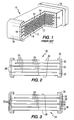
- Figure 1 is a pictorial depiction of a prior art varistor.
- Figure 2 is a vertical cross section of an embodiment of the device of the present invention.
- Figure 3 is a vertical cross section of another embodiment of the device of the present invention.
- FIG. 2 shows an embodiment of a nonlinear resistive element 20 that include a body 22 having stacked zinc oxide semiconductor layers 24 with generally planar electrodes 26 between adjacent pairs of layers 24.
- the zinc oxide layers 24 need not be comprised of pure zinc oxide and may be comprised of a ceramic consisting principally of zinc oxide.
- Each electrode 26 may have a contactable portion 28 that is exposed for electrical connection to nickel barrier end terminations 30 that cover terminal regions 32 of the body 22 and contact the electrodes 26.
- the exterior portion of body 22 not covered with the end terminations 30 remain as exposed zinc oxide surface 38.
- Nickel barrier end terminations 30 may be plated with layers 34 of electrically conductive, solderable tin or tin-lead metal that form electrically contactable solderable end portions for the resistive element 20.
- FIG 3 shows another embodiment of a nonlinear resistive manufactured using the method of the present invention
- element 20 includes body 22 having stacked zinc oxide semiconductor layers 24 and generally planar electrodes 26 between adjacent pairs of layers 24.
- Each electrode 26 may have a contactable portion 28 exposed for electrical connection to a first electrically conductive metal (preferably silver, platinum-free silver, or palladium-free silver) end terminations 36 with nickel barrier end terminations 30 thereupon, covering terminal regions 32 and extending a desired distance along the body 22.
- nickel barrier end terminations 30 may be plated with layers 34 of solderable tin or tin-lead metal that form final electrically contactable end portions for the resistive element 20.
- the zinc oxide layers 24 may have the following composition in mole percent: 94-98% zinc oxide and 2-6% of one or more of the following additives; bismuth oxide, cobalt oxide, manganese oxide, nickel oxide, antimony oxide, boric oxide, chromium oxide, silicon oxide, aluminum nitrate, and other equivalents.
- the body 22 is provided conventionally, electrodes 26 having contactable portions 28 exposed for electrical connection at terminal regions 32 with the remaining portions of body 22 being exposed zinc oxide surface 38.
- Process parameter control to avoid process boundary problems including: 1) plating not occurring, 2) plating not uniformly covering terminal regions 32, 3) plating too thick or thin; and 4) plating spread beyond the desired terminal region 32 onto exposed zinc oxide surface 38, requires the selection of nickel plating solution appropriate for an intended method of nickel barrier end termination plating-electro-plating electroless plating, or brush plating. Having determined the method of nickel plating, an end of body 22 controllable contacts the nickel plating solution to form a desirably thick nickel barrier end terminations 30 over terminal region 32.
- Complimentary parameter processes selection, identification of nickel plating solution, plating method, and controllable contact assures that nickel barrier end terminations 30 uniformly cover terminal region 32 without extending undesirably along exposed surface 38 and while avoiding unacceptable zinc oxide etching, which etching is known to cause electrical leakage currents and mechanical weakness in the final device.
- the method of the present invention allows the temperature of the nickel plating solution to remain uncontrolled such that the solution remains at approximately room temperature.
- the pH of the nickel plating solution may be maintained between 2 and 6.
- Contact between semiconductor body 22 and nickel plating solution may vary from 15 to 120 minutes to allow the formation of end termination 30 with a thickness between 1 and 3 um.
- solderable contact 34 over end termination 30 by controllably immersing the nickel termination 30 into a room temperature solution containing one of Alkyl-tin, Alkyl-tin-lead, Tin-Lead sulfuric acid, or tin sulfuric acid having a pH from 2 to 6.
- the partial immersion may vary in the range from 10 to 120 minutes to allow the formation of solderable contact 34 with a cap thickness ranging from 3 to 6 um.
- solderable contact plating may include application of a biasing current of approximately 0.3 to 2.0 A/dm 2 .
- a nickel plating solution comprising a room temperature solution of nickel sulphate, dimethylamineborane, lactic acid, ammonium citrate, and ammonia may be used in combination with semiconductor body 22 having zinc oxide layers 24 with a resistivity in the range from 10 10 to 10 12 Ohms/cm.
- the pH of the nickel plating solution may be maintained between 2 and 6.
- one end of semiconductor body 22 is positioned a selectable distance into the nickel plating solution covering that end of body 22 and allowing the plating solution to travel up a portion of exposed zinc oxide surface 38. Maintaining body 22 immersed for a period of 15 to 120 minutes provides for a nickel cap between 1 and 3 um.
- a suitable absorbent material is impregnated with the nickel plating solution.
- One end of semiconductor body 22 is placed in contact with the impregnated absorbent material such that terminal region 32 completely contacts the absorbent material.
- Pressure between body 22 and absorbent material is maintained to allow formation of nickel end termination 30 on terminal region 32 and a desired distance along exposed zinc surface 38.
- the contact period may vary between 15 and 120 minutes to control termination 30 thickness and travel up surface 38. Relative motion may be provided so that semiconductor body 22 moves relative to the absorbent material.
- a first electrically conductive metal end termination 36 is provided intermediate end termination 30 and body 20 and further includes providing a nickel plating solution comprising one of nickel sulphate or nickel chloride, boric acid, a wetting agent, and a stress relieving agent with the plating solution maintained at a temperature of 50 to 70°C.
- First end termination 36 material may preferably comprise silver, platinum-free silver, and/or palladium-free silver and glass frit. The use of platinum-free and/or palladium-free silver reduces the cost of device manufacture.
- the silver/glass frit material may be conventionally applied onto opposing ends of body 20 and fired to mechanically bond the silver/glass frit materials to terminal regions 32 forming first end terminations 36. Firing temperatures of 550 to 800°C have provided favorable results.
- Body 20 with first end termination 36 is partially immersed into the nickel plating solution for a period from 15 to 120 minutes while applying biasing current of 0.3 to 2.0 A/dm 2 .
- biasing current 0.3 to 2.0 A/dm 2 .
- a final solderable termination may be provided over nickel end termination 30 using a room temperature solution of one of Alkyl-tin, Alkyl-tin-lead, Tin-Lead sulfuric acid, or tin sulfuric acid.
- Solder plating solutions having a pH in the range of approximately 3 to 6 have been suitable when layers 34 are formed with an immersion period ranging from 10 to 120 minutes and a biasing current of 0.3 to 2.0 A/dm 2 .
- solder leaching is minimized without the use of more expensive platinum or palladium by coating first end termination 36 with nickel termination 30 so as to avoid silver leaching when the varistor device is soldered to a board.
- a method of providing nickel barrier end terminations for a zinc oxide semiconductor device with exposed body surfaces and end terminal regions in which the device is controllably reacted with a nickel plating solution only on an exposed end terminal region and thereafter provided with a final tin or tin-lead termination.
Landscapes
- Engineering & Computer Science (AREA)
- Microelectronics & Electronic Packaging (AREA)
- Physics & Mathematics (AREA)
- Electromagnetism (AREA)
- Manufacturing & Machinery (AREA)
- Electroplating Methods And Accessories (AREA)
- Electroplating And Plating Baths Therefor (AREA)
- Apparatuses And Processes For Manufacturing Resistors (AREA)
- Thermistors And Varistors (AREA)
- Chemically Coating (AREA)
Priority Applications (3)
| Application Number | Priority Date | Filing Date | Title |
|---|---|---|---|
| GB9813796A GB2326976A (en) | 1997-06-30 | 1998-06-25 | Varistor nickel barrier electrode |
| JP10184993A JPH11106938A (ja) | 1997-06-30 | 1998-06-30 | ニッケルバリアの末端終結部および方法 |
| EP98305676A EP0973176A1 (de) | 1997-06-30 | 1998-07-16 | Anschlusskontakt mit Nickelbarriere und Verfahren |
Applications Claiming Priority (2)
| Application Number | Priority Date | Filing Date | Title |
|---|---|---|---|
| US08/885,859 US6232144B1 (en) | 1997-06-30 | 1997-06-30 | Nickel barrier end termination and method |
| EP98305676A EP0973176A1 (de) | 1997-06-30 | 1998-07-16 | Anschlusskontakt mit Nickelbarriere und Verfahren |
Publications (1)
| Publication Number | Publication Date |
|---|---|
| EP0973176A1 true EP0973176A1 (de) | 2000-01-19 |
Family
ID=26151348
Family Applications (1)
| Application Number | Title | Priority Date | Filing Date |
|---|---|---|---|
| EP98305676A Withdrawn EP0973176A1 (de) | 1997-06-30 | 1998-07-16 | Anschlusskontakt mit Nickelbarriere und Verfahren |
Country Status (3)
| Country | Link |
|---|---|
| EP (1) | EP0973176A1 (de) |
| JP (1) | JPH11106938A (de) |
| GB (1) | GB2326976A (de) |
Families Citing this family (5)
| Publication number | Priority date | Publication date | Assignee | Title |
|---|---|---|---|---|
| US7152291B2 (en) | 2002-04-15 | 2006-12-26 | Avx Corporation | Method for forming plated terminations |
| US7463474B2 (en) | 2002-04-15 | 2008-12-09 | Avx Corporation | System and method of plating ball grid array and isolation features for electronic components |
| US6982863B2 (en) * | 2002-04-15 | 2006-01-03 | Avx Corporation | Component formation via plating technology |
| US7177137B2 (en) | 2002-04-15 | 2007-02-13 | Avx Corporation | Plated terminations |
| US7576968B2 (en) | 2002-04-15 | 2009-08-18 | Avx Corporation | Plated terminations and method of forming using electrolytic plating |
Citations (6)
| Publication number | Priority date | Publication date | Assignee | Title |
|---|---|---|---|---|
| JPS57105962A (en) * | 1980-12-24 | 1982-07-01 | Kuranobu Sugita | Manufacture of sintered nickel electrode by lectrolytic impregnation |
| EP0092971A1 (de) * | 1982-04-27 | 1983-11-02 | Richardson Chemical Company | Verfahren zum selektiven Abscheiden einer Nickel-Bor Schicht über einem metallurgischen Muster auf einem dielektrischen Substrat und auf diese Weise hergestellte Produkte |
| EP0716429A2 (de) * | 1994-12-09 | 1996-06-12 | Harris Corporation | Zinkphosphat-Beschichtung für Varistor und Verfahren zu ihrer Herstellung |
| JPH09246017A (ja) * | 1996-03-07 | 1997-09-19 | Tdk Corp | 積層型チップバリスタ及びその製造方法 |
| DE19634488A1 (de) * | 1996-08-26 | 1998-03-05 | Siemens Matsushita Components | Elektro-keramisches Bauelement und Verfahren zu seiner Herstellung |
| JPH10172807A (ja) * | 1996-12-12 | 1998-06-26 | Mitsubishi Materials Corp | サーミスタの製造方法 |
Family Cites Families (3)
| Publication number | Priority date | Publication date | Assignee | Title |
|---|---|---|---|---|
| DE3930000A1 (de) * | 1988-09-08 | 1990-03-15 | Murata Manufacturing Co | Varistor in schichtbauweise |
| EP0412259B1 (de) * | 1989-06-16 | 1995-09-27 | Matsushita Electric Industrial Co., Ltd. | Elektronische Verbindungen, Verfahren zur Bildung von Endverbindern dafür und Paste zur Ausbildung derselben |
| EP0806780B1 (de) * | 1996-05-09 | 2000-08-02 | Littlefuse, Inc. | Zink-Phosphatbeschichtung für Varistor und Verfahren zur Herstellung |
-
1998
- 1998-06-25 GB GB9813796A patent/GB2326976A/en not_active Withdrawn
- 1998-06-30 JP JP10184993A patent/JPH11106938A/ja active Pending
- 1998-07-16 EP EP98305676A patent/EP0973176A1/de not_active Withdrawn
Patent Citations (6)
| Publication number | Priority date | Publication date | Assignee | Title |
|---|---|---|---|---|
| JPS57105962A (en) * | 1980-12-24 | 1982-07-01 | Kuranobu Sugita | Manufacture of sintered nickel electrode by lectrolytic impregnation |
| EP0092971A1 (de) * | 1982-04-27 | 1983-11-02 | Richardson Chemical Company | Verfahren zum selektiven Abscheiden einer Nickel-Bor Schicht über einem metallurgischen Muster auf einem dielektrischen Substrat und auf diese Weise hergestellte Produkte |
| EP0716429A2 (de) * | 1994-12-09 | 1996-06-12 | Harris Corporation | Zinkphosphat-Beschichtung für Varistor und Verfahren zu ihrer Herstellung |
| JPH09246017A (ja) * | 1996-03-07 | 1997-09-19 | Tdk Corp | 積層型チップバリスタ及びその製造方法 |
| DE19634488A1 (de) * | 1996-08-26 | 1998-03-05 | Siemens Matsushita Components | Elektro-keramisches Bauelement und Verfahren zu seiner Herstellung |
| JPH10172807A (ja) * | 1996-12-12 | 1998-06-26 | Mitsubishi Materials Corp | サーミスタの製造方法 |
Non-Patent Citations (3)
| Title |
|---|
| PATENT ABSTRACTS OF JAPAN vol. 006, no. 194 (E - 134) 2 October 1982 (1982-10-02) * |
| PATENT ABSTRACTS OF JAPAN vol. 098, no. 001 30 January 1998 (1998-01-30) * |
| PATENT ABSTRACTS OF JAPAN vol. 098, no. 011 30 September 1998 (1998-09-30) * |
Also Published As
| Publication number | Publication date |
|---|---|
| JPH11106938A (ja) | 1999-04-20 |
| GB9813796D0 (en) | 1998-08-26 |
| GB2326976A (en) | 1999-01-06 |
Similar Documents
| Publication | Publication Date | Title |
|---|---|---|
| EP0969481A1 (de) | Zink-Phosphatbeschichtung für Varistor und Verfahren zur Herstellung | |
| US6232144B1 (en) | Nickel barrier end termination and method | |
| EP0716429B1 (de) | Zinkphosphat-Beschichtung für Varistor und Verfahren zu ihrer Herstellung | |
| JP4143539B2 (ja) | 複数のコンタクト面を有するエレクトロセラミックス構成素子 | |
| EP0181032B1 (de) | Festelektrolytkondensator für Oberflächenmontage | |
| KR100350184B1 (ko) | 모놀리식 배리스터의 제조 방법 | |
| JP3497840B2 (ja) | ガラスコーティング膜を有するチップバリスタの製造方法 | |
| US5036434A (en) | Chip-type solid electrolytic capacitor and method of manufacturing the same | |
| WO2001037296A1 (en) | Solid state capacitors and methods of manufacturing them | |
| KR102798602B1 (ko) | 향상된 연결성을 갖는 다층 전자 디바이스 및 다층 전자 디바이스의 제조 방법 | |
| US4794491A (en) | Solid electrolyte capacitor | |
| US6841191B2 (en) | Varistor and fabricating method of zinc phosphate insulation for the same | |
| US4164005A (en) | Solid electrolyte capacitor, solderable terminations therefor and method for making | |
| EP0973176A1 (de) | Anschlusskontakt mit Nickelbarriere und Verfahren | |
| US5168434A (en) | Fuse-incorporated, chip-type solid electrolytic capacitor | |
| EP0806780B1 (de) | Zink-Phosphatbeschichtung für Varistor und Verfahren zur Herstellung | |
| EP0090634A2 (de) | Mehrschichtkondensatoren mit keramischen Dielektrikum | |
| US6278065B1 (en) | Apparatus and method for minimizing currents in electrical devices | |
| US4450502A (en) | Multilayer ceramic dielectric capacitors | |
| EP0072126A2 (de) | Mehrlagige Kondensatoren mit Keramikdielektrikum | |
| JPS634327B2 (de) | ||
| CN1241007A (zh) | 镍阻挡端部及形成方法 | |
| JPS638605B2 (de) | ||
| JPH05129105A (ja) | チツプ・バリスタ | |
| JPS6228746Y2 (de) |
Legal Events
| Date | Code | Title | Description |
|---|---|---|---|
| PUAI | Public reference made under article 153(3) epc to a published international application that has entered the european phase |
Free format text: ORIGINAL CODE: 0009012 |
|
| AK | Designated contracting states |
Kind code of ref document: A1 Designated state(s): AT DE FR IE IT |
|
| AX | Request for extension of the european patent |
Free format text: AL;LT;LV;MK;RO;SI |
|
| 17P | Request for examination filed |
Effective date: 20000719 |
|
| AKX | Designation fees paid |
Free format text: AT DE FR IE IT |
|
| 17Q | First examination report despatched |
Effective date: 20011113 |
|
| STAA | Information on the status of an ep patent application or granted ep patent |
Free format text: STATUS: THE APPLICATION IS DEEMED TO BE WITHDRAWN |
|
| 18D | Application deemed to be withdrawn |
Effective date: 20040202 |